
Effect of Pd/ZnO Morphology on Surface Acoustic Wave Sensor Response


Abstract
:1. Introduction
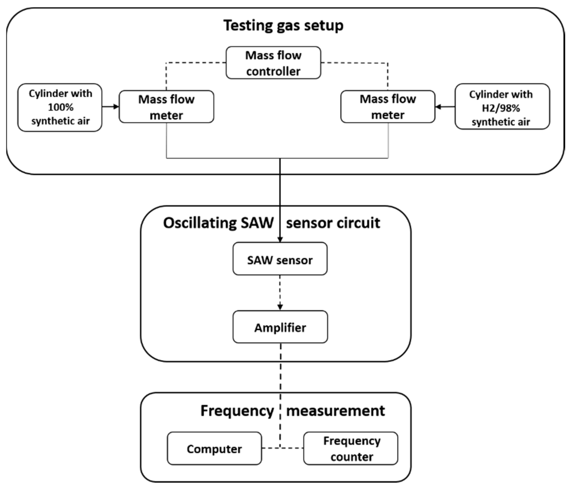
2. Materials and Methods
3. Results and Discussion
3.1. Film Morphology
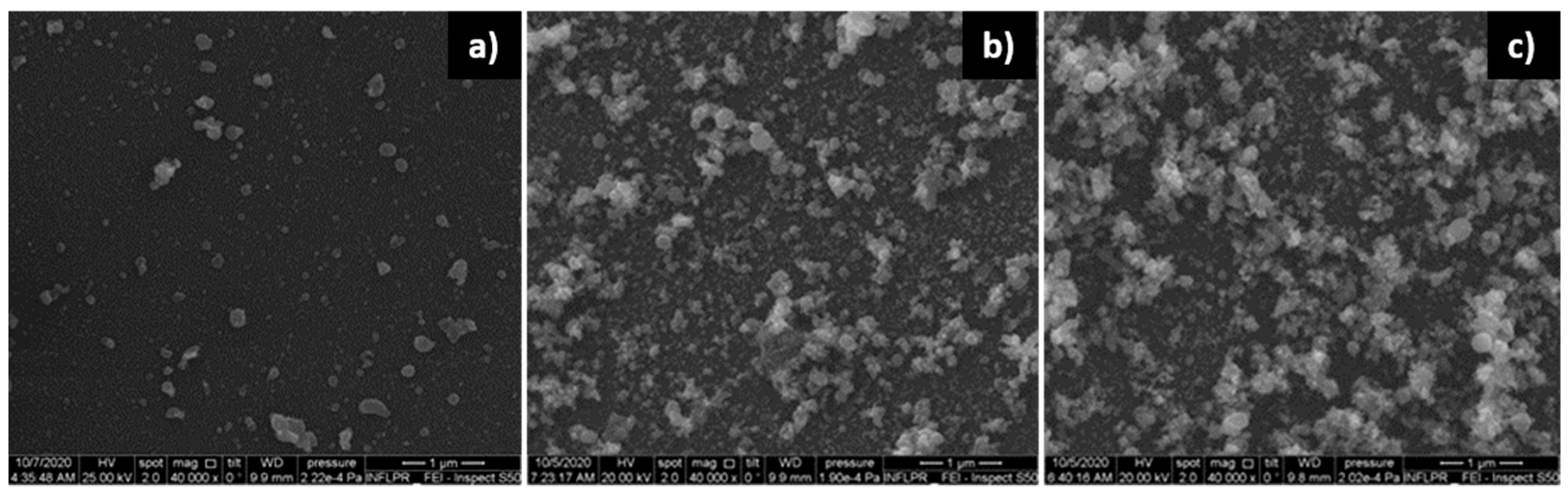
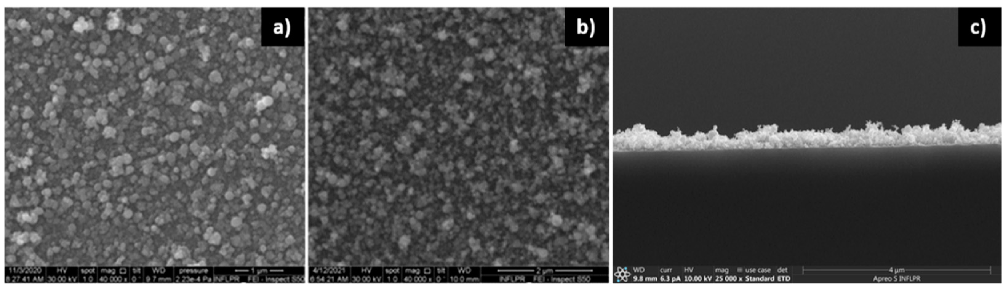
3.1.1. ZnO Films
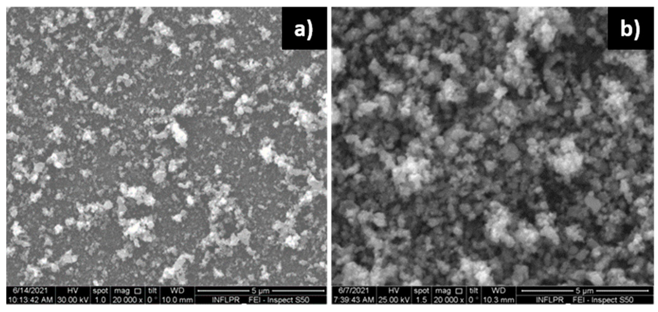
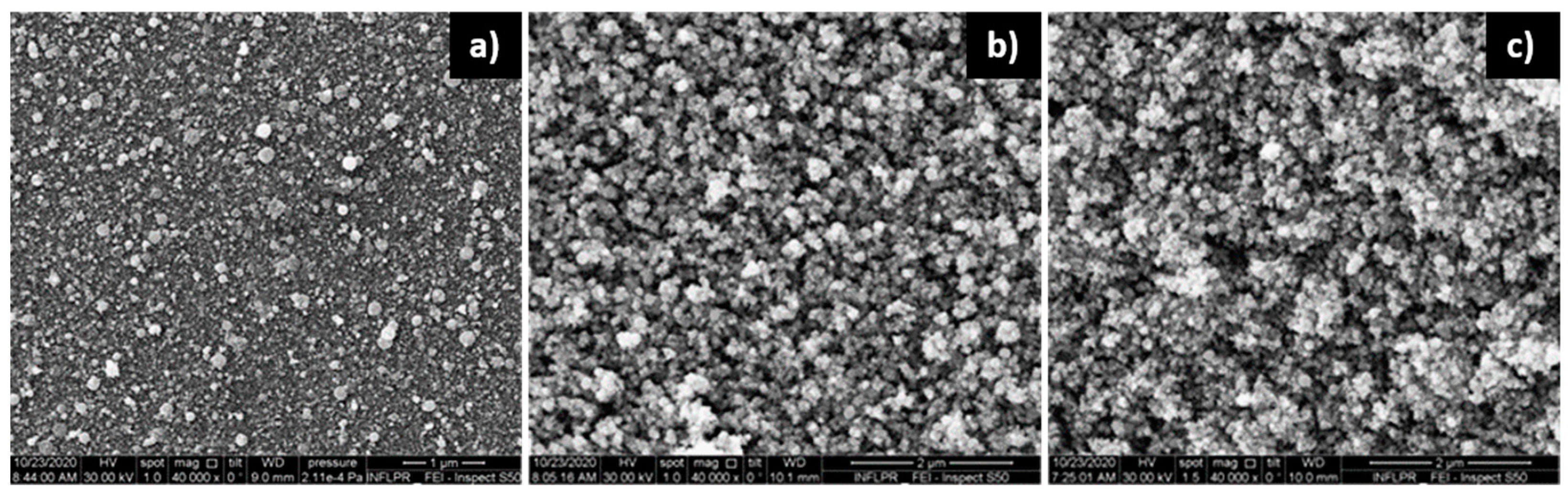
3.1.2. Pd Films
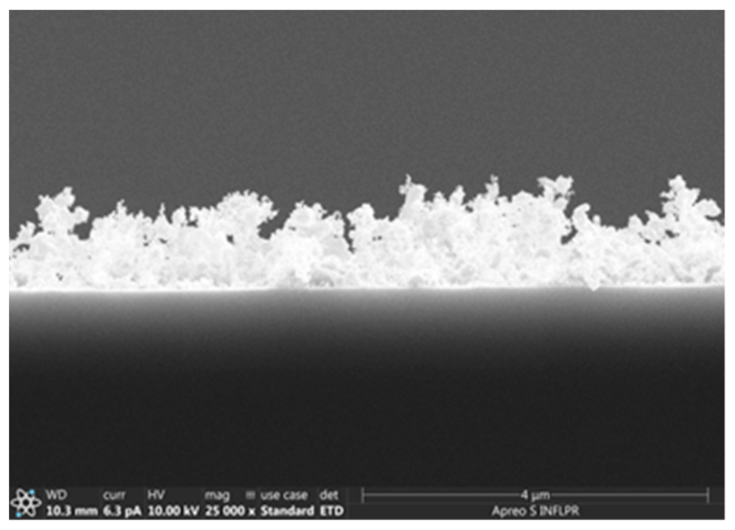
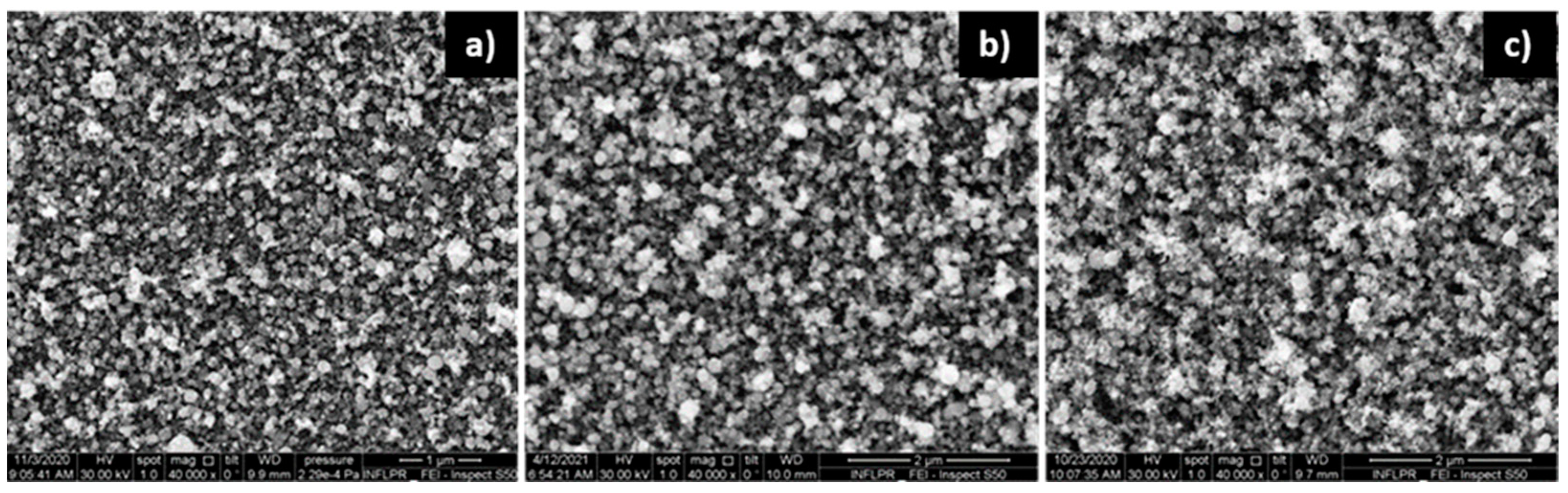
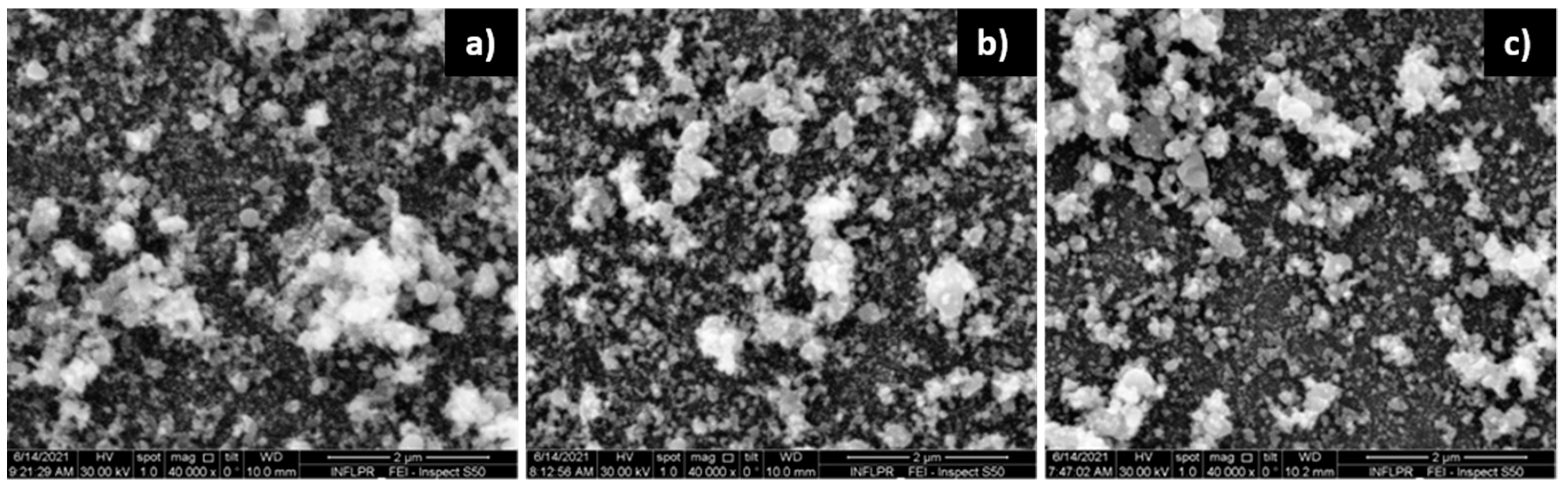
3.1.3. Pd/ZnO Bilayer
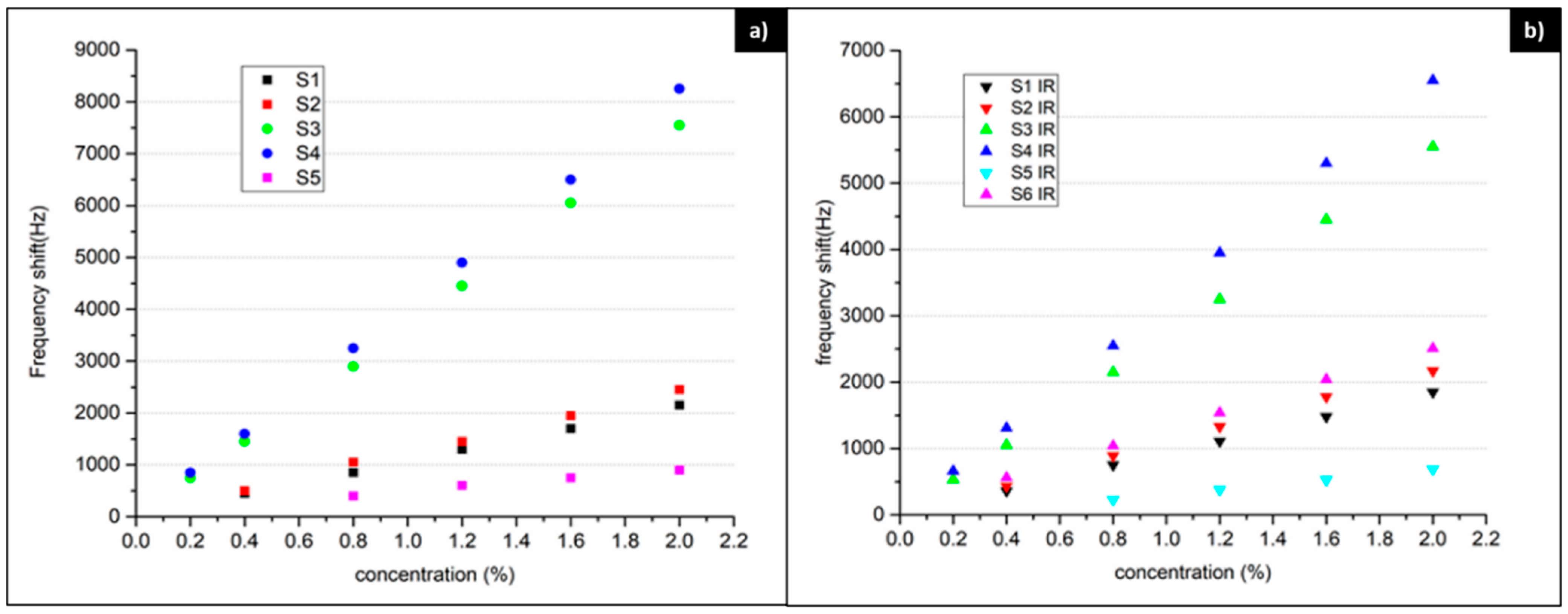
3.2. Sensor Properties
4. Conclusions
Supplementary Materials
Author Contributions
Funding
Institutional Review Board Statement
Informed Consent Statement
Data Availability Statement
Acknowledgments
Conflicts of Interest
References
- Xu, H.; Liu, Y.; Liu, H.; Dong, S.; Wu, Y.; Wang, Z.; Wang, Y.; Wu, M.; Han, Z.; Hao, L. Pd-decorated 2D SnSe ultrathin film on SiO2/Si for room-temperature hydrogen detection with ultrahigh response. J. Alloy. Compd. 2020, 851, 156844. [Google Scholar] [CrossRef]
- Li, Z.; Yao, Z.; Haidry, A.A.; Plecenik, T.; Xie, L.; Sun, L.; Fatima, Q. Resistive-type hydrogen gas sensor based on TiO2: A review. Int. J. Hydrog. Energy 2018, 43, 21114–21132. [Google Scholar] [CrossRef]
- Okolie, J.A.; Patra, B.R.; Mukherjee, A.; Nanda, S.; Dalai, A.K.; Kozinski, J.A. Futuristic applications of hydrogen in energy, biorefining, aerospace, pharmaceuticals and metallurgy. Int. J. Hydrog. Energy 2021, 46, 8885–8905. [Google Scholar] [CrossRef]
- Chen, K.; Yuan, D.; Zhao, Y. Review of optical hydrogen sensors based on metal hydrides: Recent developments and challenges. Opt. Laser Technol. 2020, 137, 106808. [Google Scholar] [CrossRef]
- Liu, W.; Zuo, H.; Wang, J.; Xue, Q.; Ren, B.; Yang, F. The production and application of hydrogen in steel industry. Int. J. Hydrog. Energy 2021, 46, 10548–10569. [Google Scholar] [CrossRef]
- Kima, J.-H.; Mirzaei, A.; Kim, H.W.; Kim, S.S. Improving the hydrogen sensing properties of SnO2 nanowire-based conductometric sensors by Pd-decoration. Sens. Actuators B. Chem. 2019, 285, 358–367. [Google Scholar] [CrossRef]
- Nikolaeva, N.S.; Klyamer, D.D.; Zharkov, S.M.; Tsygankova, A.R.; Sukhikh, A.S.; Morozova, N.B.; Basova, T.V. Heterostructures based on PdeAu nanoparticles and cobalt phthalocyanine for hydrogen chemiresistive sensors. Int. J. Hydrog. Energy 2021, 46, 19682–19692. [Google Scholar] [CrossRef]
- Wang, W.; Liu, X.; Mei, S.; Jia, Y.; Liu, M.; Xue, X.; Yang, D. Deveopment of Pd/Cu nanowires coated SAW hydrogen gas sensor with fast response and recovery. Sens. Actuators B Chem. 2019, 287, 157–164. [Google Scholar] [CrossRef]
- Constantinoiu, I.; Viespe, C. Hydrogen Detection with SAW Polymer/Quantum Dots Sensitive Films. Sensors 2019, 19, 4481. [Google Scholar] [CrossRef] [Green Version]
- Ballantine, D.S.; White, R.M.; Martin, S.J.; Ricco, A.J.; Zellers, E.T.; Frye, G.C.; Wohtjen, H. Acoustic Wave Sensors, Theory, Design and Physico-Chemical Applications; Academic Press: San Diego, CA, USA, 1997. [Google Scholar]
- Panneerselvam, G.; Thirumal, V.; Pandya, H.M. Review of Surface Acoustic Wave Sensors for the Detection and Identification od Toxic Environmental Gases/Vapours. Arch. Acoust. 2018, 43, 357–367. [Google Scholar]
- Kus, F.; Altinkok, C.; Zayim, E.; Erdemir, S.; Tasaltin, C.; Gurol, I. Surface acoustic wave (SAW) sensor for volatile organic compounds (VOCs) detection with calix[4]arene functionalized Gold nanorods (AuNRs) and silver nanocubes (AgNCs). Sens. Actuators B Chem. 2020, 330, 129402. [Google Scholar] [CrossRef]
- Matatagui, D.; Gràcia, I.; Horrillo, M. Response of a SAW Sensor Array based on Nanoparticles for Measuring Ammonia in the Environment. In Proceedings of the 9th International Conference on Sensor Networks—SENSORNETS, Valletta, Malta, 28–29 February 2020; pp. 93–99, ISBN 978-989-758-403-9. [Google Scholar] [CrossRef]
- Tanga, Y.; Xu, X.; Han, S.; Cai, C.; Du, H.; Zhu, H.; Zu, X.; Fu, Y. ZnO-Al2O3 nanocomposite as a sensitive layer for high performance surface acoustic wave H2S gas sensor with enhanced elastic loading effect. Sens. Actuators B. Chem. 2020, 304, 127395. [Google Scholar] [CrossRef]
- Harathi, N.; Kavitha, S.; Sarkar, A. ZnO nanostructured 2D layered SAW based hydrogen gas sensor with enhanced sensitivity. Mater. Today Proc. 2020, 33, 2621–2625. [Google Scholar] [CrossRef]
- Constantinoiu, I.; Viespe, C. Development of Pd/TiO2 Porous Layers by Pulsed Laser Deposition for Surface Acoustic Wave H2 Gas Sensor. Nanomaterials 2020, 10, 760. [Google Scholar] [CrossRef] [PubMed] [Green Version]
- Constantinoiu, I.; Miu, D.; Viespe, C. Surface Acoustic Wave Sensors for Ammonia Detection at Room Temperature Based on SnO2/Co3O4 Bilayers. J. Sens. 2019, 2019, 1–6. [Google Scholar] [CrossRef] [Green Version]
- Sima, C.; Viespe, C. Surface Acoustic Wave Sensors Based on Nanoporous SnO2 Films for Hydrogen Detection; Chemical Sensors and Biosensors: Barcelona, Spain, 2018. [Google Scholar]
- Ozturk, S.; Kilimc, N. Pd thin films on flexible substrate for hydrogen sensor. J. Alloy. Compd. 2016, 674, 179–184. [Google Scholar] [CrossRef]
- Li, D.; Le, X.; Pang, J.; Peng, L.; Xu, Z.; Gao, C.; Xie, J. A SAW hydrogen sensor based on decoration of graphene oxide by palladium nanoparticles on AIN/Si layered structure. J. Micromech. Microeng. 2019, 29, 45007. [Google Scholar] [CrossRef]
- Groenen, R.; Smit, J.; Orsel, K.; Vailionis, A.; Bastiaens, H.M.; Huijben, M.; Boller, K.J.; Rijnders, A.J.; Koster, G. Research update: Stoichiometry controlled oxide thin film growth by pulsed laser deposition. APL Mater. 2015, 3, 70701. [Google Scholar] [CrossRef]
- Cheng, P.; Wang, L.; Pan, Y.; Yan, H.; Gao, D.; Wang, J.; Zhang, H. Fiber Bragg grating temperature sensor of cladding with SrTiO3 thin film by pulsed laser deposition. Laser Phys. 2019, 29, 25107. [Google Scholar] [CrossRef]
- Slaiby, Z.E.; Ramizy, A. Synthesis gallium nitride thin films by pulsed laser deposition as ammonia (NH3) gas sensor. J. Optoelectron. Biomed. Mater. 2020, 12, 17–23. [Google Scholar]
- Dekic, M.; Salcinovic Fetic, A.; Hrvat, K.; Lozancic, M. Influence of deposition parameters on pulsed laser deposition of K0.3MoO3 thin films. Bull. Chem. Technol. Bosnia Herzeg. 2017, 48, 1–4. [Google Scholar]
- Viespe, C.; Miu, D. Surface Acoustic Wave Sensor with Pd/ZnO Bilayer Sructure for Room Temperature Hydrogen Detection. Sensors 2017, 17, 1529. [Google Scholar] [CrossRef]
- Sanger, A.; Kumar, A.; Kumar, A.; Jaiswal, J.; Chandra, R. A fast response/recovery of hydrophobic Pd/V2O5 thin films for hydrogen gas sensing. Sens. Actuators B Chem. 2016, 236, 16–26. [Google Scholar] [CrossRef]
- Miu, D.; Birjega, R.; Viespe, C. Surface Acoustic Wave Hydrogen Sensors Based on Nanostructured Pd/WO3 Bilayers. Sensors 2018, 18, 3636. [Google Scholar] [CrossRef] [Green Version]
- Viespe, C.; Miu, D. Characteristics of Surface Acoustic Wave Sensors with Nanoparticles Embedded in Polymer Sensitive Layers for VOC Detection. Sensors 2018, 18, 2401. [Google Scholar] [CrossRef] [PubMed] [Green Version]
- Image J Open-Source Image Processing Program; NIH: Bethesda, MD, USA, 2008.
- Geohegan, D.B.; Puretzky, A.A. Laser ablation plume thermalization dynamics in background gases: Combined imaging, optical absorption and emission spectroscopy, and ion probe measurements. Appl. Surf. Sci. 1996, 96-98, 131–138. [Google Scholar] [CrossRef] [Green Version]
- Harilal, S.S.; O’Shay, B.; Tao, Y.; Tillack, M.S. Ambient gas effects on the dynamics of laser-produced tin plume expansion. J. Appl. Phys. 2006, 99, 83303. [Google Scholar] [CrossRef] [Green Version]
- Geohegan, D.; Puretzky, A.; Duscher, G.; Pennycook, S.J. Time-resolved imaging of gas phase nanoparticle synthesis by laser ablation. Appl. Phys. Lett. 1998, 72, 2987–2989. [Google Scholar] [CrossRef] [Green Version]
- Tillack, M.S.; Blair, D.W.; Harilal, S.S. The effect of ionization on cluster formation in laser ablation plumes. Nanotechnology 2004, 15, 390–403. [Google Scholar] [CrossRef]
- Viespe, C.; Dinca, V.; Popescu-Pelin, G.; Miu, D. Love Wave Surface Acoustic Wave Sensor with Laser-Deposited Nanoporous Gold Sensitive Layer. Sensors 2019, 19, 4492. [Google Scholar] [CrossRef] [PubMed] [Green Version]


| Sensor | Deposition Wavelength (nm) | O2 Pressure—ZnO Deposition (mTorr) | Ar Pressure—Pd Deposition (mTorr) |
|---|---|---|---|
| S1 | 532 | 100 | 100 |
| S2 | 532 | 100 | 700 |
| S3 | 532 | 700 | 100 |
| S4 | 532 | 700 | 700 |
| S5 | 532 | 100 | - |
| S1 IR | 1064 | 100 | 100 |
| S2 IR | 1064 | 100 | 700 |
| S3 IR | 1064 | 700 | 100 |
| S4 IR | 1064 | 700 | 700 |
| S5 IR | 1064 | 100 | - |
| S6 IR | 1064 | 700 | - |
| 532 nm | 1064 nm | ||||
|---|---|---|---|---|---|
| Sensor | Sensitivity (Δf/c) (Hz/ppm) | LOD (3×n)/ (Δf/c) (ppm) | Sensor | Sensitivity (Δf/c) (Hz/ppm) | LOD (3×n)/ (Δf/c) (ppm) |
| S1 | 0.108 | 138.67 | S1 IR | 0.0923 | 162.6 |
| S2 | 0.124 | 241.37 | S2 IR | 0.1099 | 273.06 |
| S3 | 0.371 | 80.85 | S3 IR | 0.2705 | 110.93 |
| S4 | 0.41 | 73.22 | S4 IR | 0.3274 | 91.64 |
| S5 | 0.048 | 312.7 | S5 IR | 0.032 | 468.6 |
| S6 IR | 0.1303 | 230.3 | |||
Publisher’s Note: MDPI stays neutral with regard to jurisdictional claims in published maps and institutional affiliations. |
© 2021 by the authors. Licensee MDPI, Basel, Switzerland. This article is an open access article distributed under the terms and conditions of the Creative Commons Attribution (CC BY) license (https://creativecommons.org/licenses/by/4.0/).
Share and Cite
Miu, D.; Constantinoiu, I.; Enache, C.; Viespe, C. Effect of Pd/ZnO Morphology on Surface Acoustic Wave Sensor Response. Nanomaterials 2021, 11, 2598. https://doi.org/10.3390/nano11102598
Miu D, Constantinoiu I, Enache C, Viespe C. Effect of Pd/ZnO Morphology on Surface Acoustic Wave Sensor Response. Nanomaterials. 2021; 11(10):2598. https://doi.org/10.3390/nano11102598
Chicago/Turabian StyleMiu, Dana, Izabela Constantinoiu, Cornelia Enache, and Cristian Viespe. 2021. "Effect of Pd/ZnO Morphology on Surface Acoustic Wave Sensor Response" Nanomaterials 11, no. 10: 2598. https://doi.org/10.3390/nano11102598
APA StyleMiu, D., Constantinoiu, I., Enache, C., & Viespe, C. (2021). Effect of Pd/ZnO Morphology on Surface Acoustic Wave Sensor Response. Nanomaterials, 11(10), 2598. https://doi.org/10.3390/nano11102598