Article

Low-Threshold Nanolaser Based on Hybrid Plasmonic Waveguide Mode Supported by Metallic Grating Waveguide Structure

1
Shandong Provincial Key Laboratory of Optics and Photonic Device & Shandong Provincial Engineering and Technical Center of Light Manipulations, School of Physics and Electronics, Shandong Normal University, Jinan 250358, China
2
Collaborative Innovation Center of Light Manipulations and Applications, Shandong Normal University, Jinan 250358, China
*
Author to whom correspondence should be addressed.
Nanomaterials 2021, 11(10), 2555; https://doi.org/10.3390/nano11102555
Submission received: 23 August 2021 / Revised: 20 September 2021 / Accepted: 25 September 2021 / Published: 29 September 2021
(This article belongs to the Section Theory and Simulation of Nanostructures)

Abstract

:
A high Q-factor of the nanocavity can effectively reduce the threshold of nanolasers. In this paper, a modified nanostructure composed of a silver grating on a low-index dielectric layer (LID) and a high-index dielectric layer (HID) was proposed to realize a nanolaser with a lower lasing threshold. The nanostructure supports a hybrid plasmonic waveguide mode with a very-narrow line-width that can be reduced to about 1.79 nm by adjusting the thickness of the LID/HID layer or the duty ratio of grating, and the Q-factor can reach up to about 348. We theoretically demonstrated the lasing behavior of the modified nanostructures using the model of the combination of the classical electrodynamics and the four-level two-electron model of the gain material. The results demonstrated that the nanolaser based on the hybrid plasmonic waveguide mode can really reduce the lasing threshold to 0.042 mJ/cm2, which is about three times lower than the nanolaser based on the surface plasmon. The lasing action can be modulated by the thickness of the LID layer, the thickness of the HID layer and the duty cycle of grating. Our findings could provide a useful guideline to design low-threshold and highly-efficient miniaturized lasers.

1. Introduction

Nanolaser based on the surface plasmon (SP) can generate a coherent high-intensity field beyond the diffraction limit [1,2], with applications in ultrasensitive sensing, spectroscopy, nonlinear optics, ultrafast on-chip sources, etc. [3,4,5,6,7,8]. However, the high radiative and ohmic loss of surface plasmon results in the higher lasing threshold. Various methods were proposed to reduce the laser threshold, such as designing new nanostructures, using new materials and so on [9,10,11,12,13]. High Q-factor indicates that the microcavity has a strong ability to restrain light and produce a higher density of states, which could enhance the interaction between light and matter, thus reducing the threshold of laser interaction [14].
Multi-layer films consisting of metal and dielectric waveguide layers can effectively reduce the loss and improve the Q factor [15,16]. In such a system, the coupling between the SP and the waveguide mode (WG) can create a hybrid resonance mode with narrow line-width and high Q factor. To obtain a low-loss hybrid mode, various plasmonic structures have been studied. For example, a multilayer dielectric under the metallic arrays can support a narrow-band transmission peak with only a few nanometers [17,18]. Li et al. proposed narrow transmission dips with the line-with of 8 nm in the dielectric grating on the semiconductor–metal–semiconductor stacks [19]. Liu et al. came up with a periodic plasmonic structure, which supports a resonance with line-width only 3 nm [20]. These resonance modes have potential applications in sensing, optical filtering, and optoelectronic devices integration because of their narrow line-width and high Q factor [21,22].
The hybrid resonance mode can also be used in the nanolaser, because it can reduce the loss effectively by concentrating the mode inside the dielectric waveguide layer, and effectively reduce the threshold of the nanolaser. In 2009, the Xiang Zhang group reported a plasmonic laser using a hybrid plasmonic waveguide that can localize the transmission mode in the micro-cavity formed by the gap layer, so the loss in the metal can be greatly reduced [23]. Degl’Innocenti et al. demonstrated the realization of the terahertz quantum cascade laser based on a hybrid plasmonic waveguide [24]. In recent years, the lasing threshold was reduced using the hybrid plasmonic waveguide mode of the nanowire waveguide mode [23,24,25,26,27,28], and the threshold of some nanolasers can be reduced to 0.2 mJ/cm2 [27].
In this paper, we investigated a hybrid plasmonic system composed of a silver grating and low-index dielectric layer (LID) coated on high-index dielectric layer (HID), and it supports a hybrid plasmonic waveguide mode with very narrow line-width and high Q factor. After we added a gain material layer composed of rhodamine 6G (R6G) onto this hybrid system, we discussed the lasing action of the nanolaser based on the hybrid plasmonic system. The results revealed that the lasing threshold of the nanolaser can be reduced to about 0.042 mJ/cm2 that is about three times lower than the nanolaser based on the surface plasmon and even lower than the previously double-layer grating dielectric waveguide structure nanolasers [29]. Furthermore, we found that the Q factor can be tuned by adjusting the thickness of the LID layer, the thickness of the HID layers and the grating duty ratio. Therefore, the lasing action can also be tuned by changing these structural parameters.

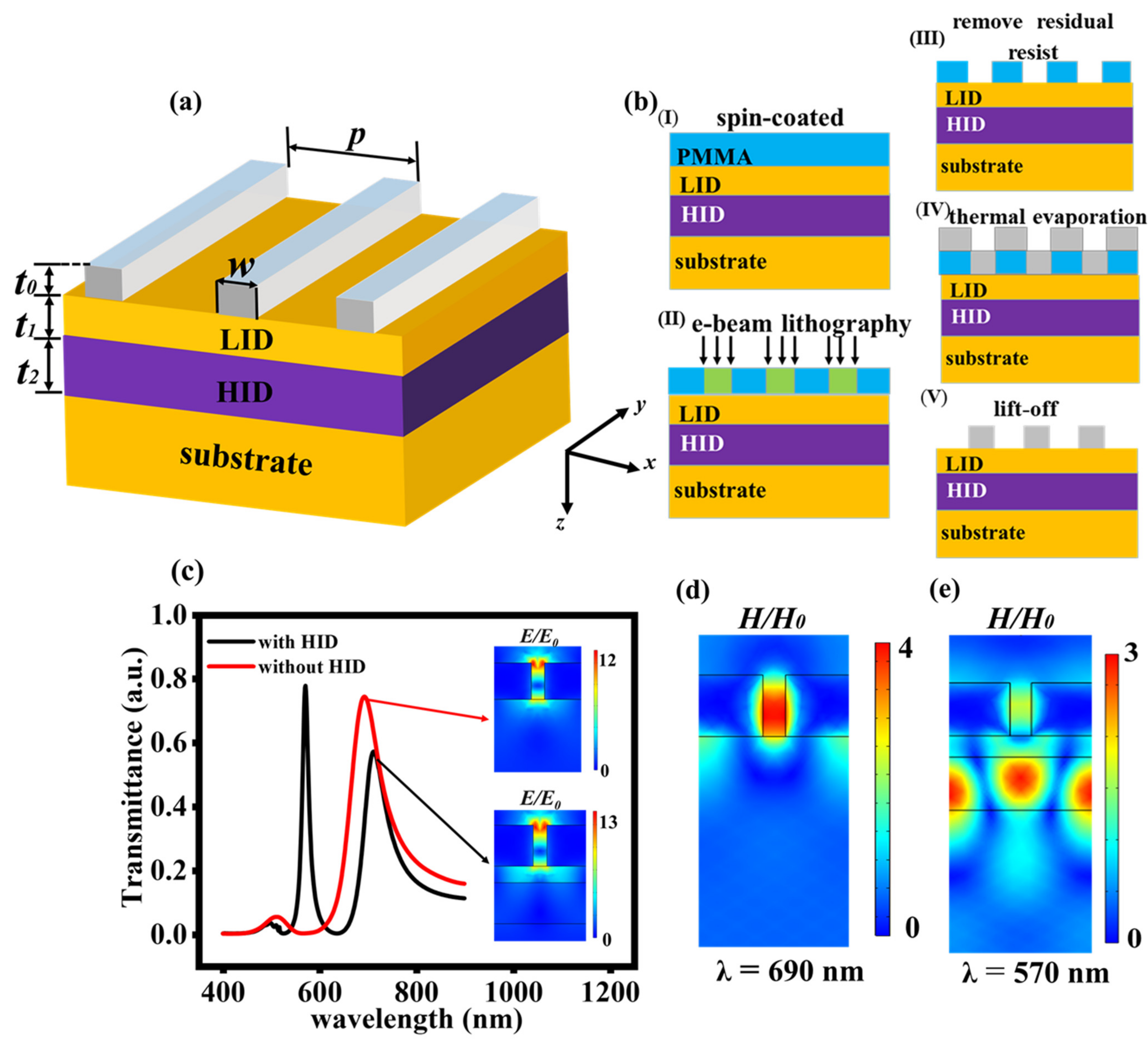
2. Materials and Methods

When LID and HID layers were introduced under a metallic nanograting (M–LH nanostructure), a resonance mode with narrower transmission peak can be obtained [30], and it is schematically displayed in Figure 1a. The refractive index of the LID layer and the substrate was set as n1 = 1.5, such as SiO2. The refractive index of HID layer was n2 = 2.0, such as TiO2 [31]. The metal was chosen as silver, and the dielectric permittivity of silver was defined by the Lorentz–Drude model, ε A g = 1 ω 2 p / ω 2 + i γ ω , where ω p and γ represent the plasma frequency and damping frequency of silver [32]; t0, t1 and t2 are the thickness of grating, LID and HID layer; p marks the grating period; w means the grating ridge width and the grating duty cycle D refers to the ratio of w to p. The finite-difference time-domain method (FDTD) was adopted to calculate the spectral characteristics and the lasing performance of the nanostructures in the following calculations. We selected one period (p = 345 nm) as the simulation domain. Bloch–Floquet periodic boundary conditions were imposed to x direction of the unit cell. In the z direction, perfectly matched layer (PML) boundary conditions were applied on the boundary of the simulation domain. A plane-wave light of transverse magnetic (TM) polarization incident normally onto the M–LH nanostructures.
Figure 1b illustrates schematically the fabrication process of the M–LH nanostructures. Firstly, we deposited an HID layer on SiO2 substrates by using magnetron sputtering equipment. Then the LID layer was sputtered onto the HID/SiO2 substrates. To fabricate the grating structure by e-beam lithography, a PMMA layer (positive resist) was spin-coated on the LID/HID/SiO2 substrate to form a resist layer. Secondly, the e-beam lithography was carried out to fabricate a grating structure using a grating pattern. Thirdly, we removed any residual resist on the substrate. Fourthly, the Ag film was deposited by thermal evaporator. Finally, Ag grating structures were obtained by a lift-off process.
Figure 1c shows the transmission spectrum of the metal grating with HID layer (black solid line) and without HID layer (red solid line). When there is no HID layer underneath the grating, only a wide peak appears at λ = 690 nm. It is a SP mode that possess high loss. Its magnetic field mainly distributes in grating layer as shown in Figure 1d. However, when the HID layer is added underneath the grating, a narrow transmission peak appears at λ = 570 nm compared with the wide nearly-null transmission of the metal nanoarrays without the HID layer. We investigated the magnetic field distribution of the resonance mode at narrow transmission peak in Figure 1e. It is a hybrid SP waveguide mode [30], and its magnetic field mainly distributes in HID layer, which leads to less loss. We used this hybrid mode to realize nanolaser with a lower threshold. For the wide peak at λ = 702.6 nm, it is still a SP mode. The resonant wavelength redshifts to 702.6 nm because of the addition of the HID layer. The intensity of the wide transmission peak decreases to 0.6 because the transmitted electric field is affected by the HID layer, as shown in the insets of the Figure 1c.

3. Results

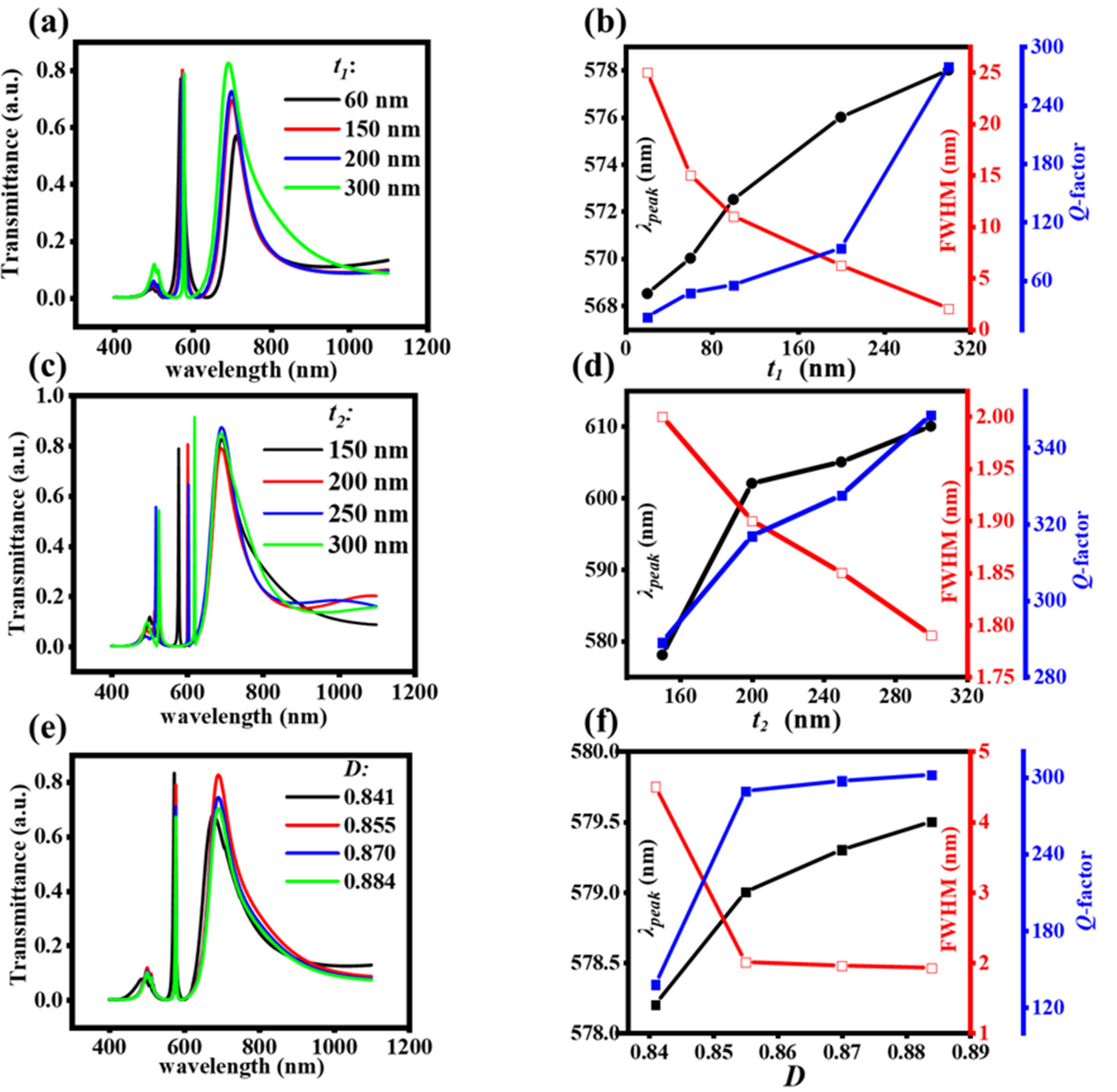
3.1. Effects of Structural Parameters on Transmission Spectrum

The full width at half maximum (FWHM) of the narrow transmission peak is affected by the thickness of the LID and HID layers [17,30,31,33,34,35], and it also can be affected by the grating duty cycle. In this part, we investigated the roles and effects of t1, t2 and D on the narrow transmission peak in Figure 2. Figure 2a shows the transmission spectra of the M–LH nanostructure with different t1, the thickness of HID layer t2 remains at 150 nm, and the grating duty cycle D remains at 0.855. As t1 increases, the position of the narrow transmission peak red shifts slightly and the FWHM becomes smaller. Figure 2b displays the dependence of the wavelength (λpeak), the FWHM and the Q factor of the narrow transmission peak on different t1. The Q factor is calculated by Q = λλ, λ is the wavelength of the resonance mode, Δλ is the FWHM of the transmission peak. The wavelength red shifts only from 568.2 to 578 nm, the line-width decreases from 25 to 2.0 nm, and the Q-factor increases from 22.7 to 289 as t1 increases from 20 to 300 nm. Figure 2c,d illustrate the influence of the thickness of the HID layer t2 on the narrow transmission peak. We chose the optimal t1 of 300 nm and D keeps 0.855. The wavelength of the narrow transmission peak red shifts a lot and the FWHM also becomes smaller when t2 increases. When t2 increases from 150 to 300 nm, the wavelength red shifts from 570 to 610 nm, the line-width decreases only from 2 to 1.79 nm, and the Q-factor increases from 289 to 348. If we choose t1 = 60 nm, the line-width of the narrow peak can decrease from 15 to 3.3 nm, and the Q-factor increases from 38 to 190 as t2 increases from 150 to 300 nm. Besides, we found that other peaks appear at smaller wavelengths, such as the peak at λ = 538 nm and λ = 542 nm for t2 = 250 and 300 nm in Figure 2c, which are the hybrid SP higher-order waveguide modes. The effects of the grating duty cycle D on the narrow peak are exhibited in Figure 2e,f, the thickness of the LID keeps 300 nm and HID layer all keeps 150 nm. The wavelength of the narrow transmission peak remains almost the same, while the FWHM becomes smaller with the increase in D. When D increases from 0.841 to 0.884, the line-width decreases from 4.2 to 1.8 nm, and the Q factor increases from 137.6 to 321.1.

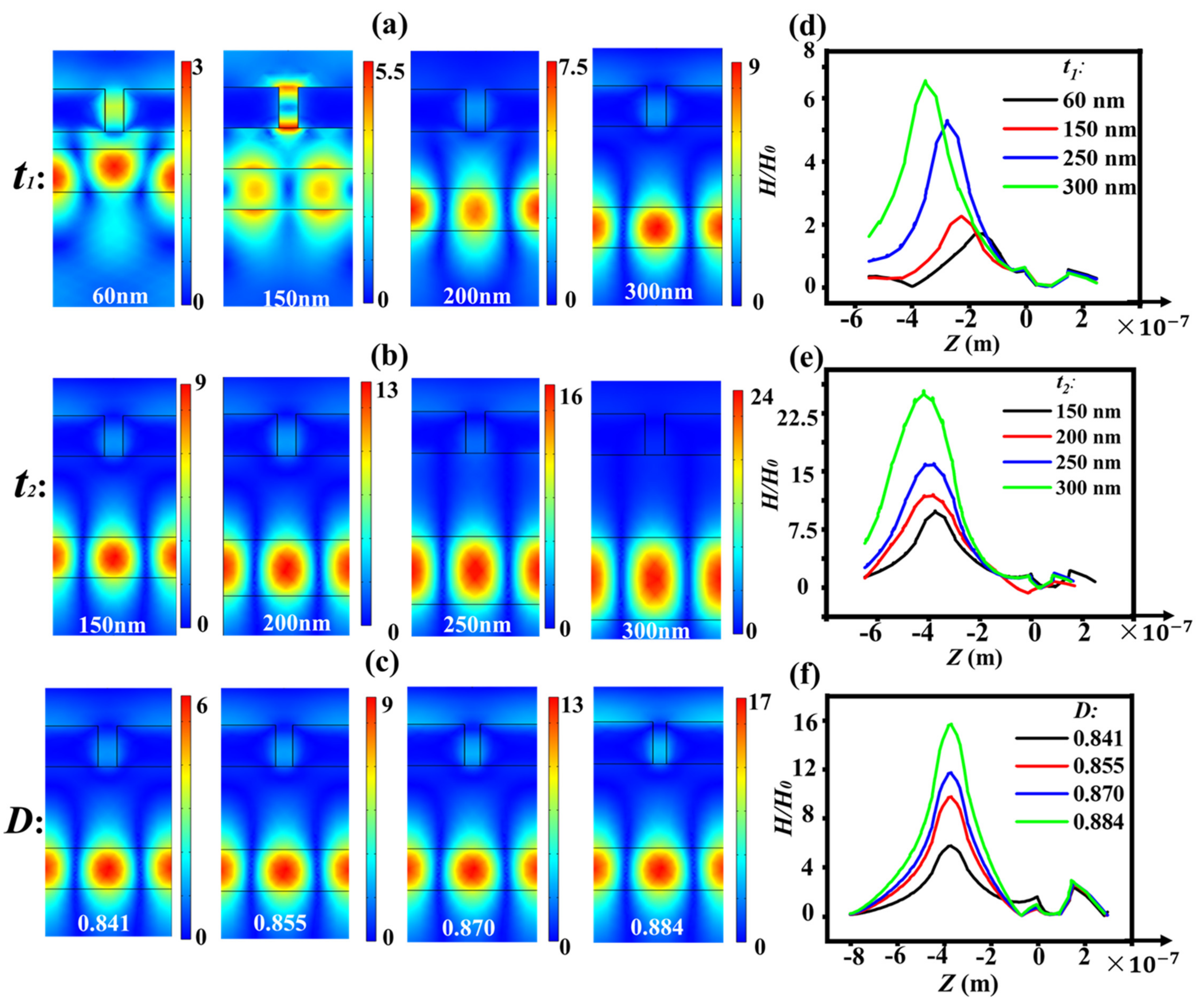
3.2. The Reasons of the Change of the Narrow Transmission Peak
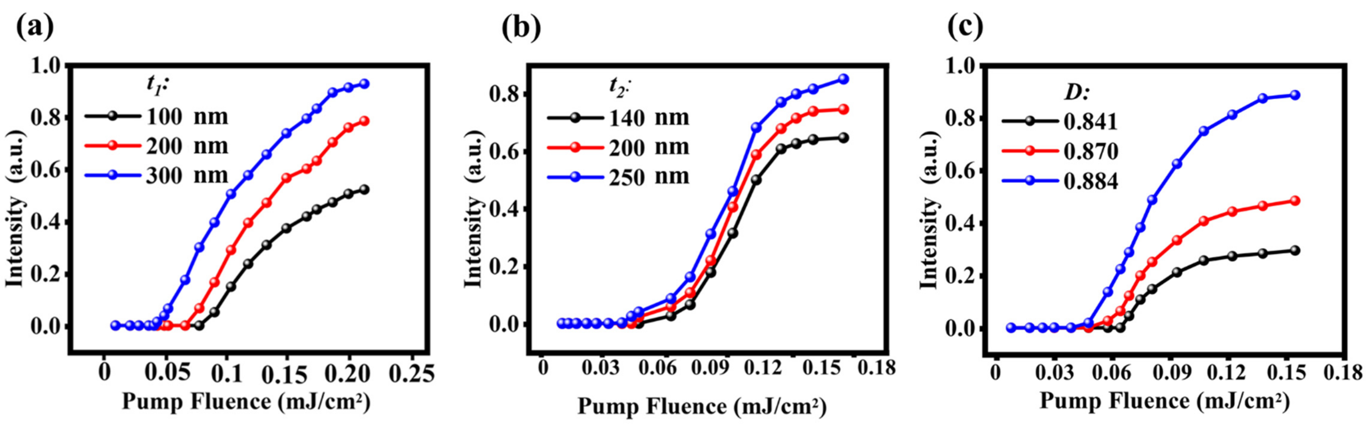
In order to investigate the reasons of the change of the narrow transmission peak with different t1, t2 and D, we plotted the field distributions (H/H0) of the M–LH nanostructures with different t1, t2 and D in Figure 3. Figure 3a exhibits the magnetic field distributions of the structure with different t1. With the increase in the thickness of LID t1, the field is more localized into the high refractive index layer. Figure 3d shows the comparison of the fields along x = 172.5 nm in Figure 3a. The intensity of the field localized in the HID layer increases gradually from 3 to 8.8. The thickness of the LID layer affects the strength of the coupling between the SP mode and waveguide mode. The larger the t1 is, the weaker the coupling is. The more field localizes into the HID layer, the weaker field at the interface of metal-LID layer is (as shown in Figure 3d), which means that the metal loss will be weakened. Therefore, the line-width of the narrow transmission peak becomes narrower, and the Q factor increases. As the position of the narrow peak mainly depends on the HID layer, the redshifts slightly are caused by the weaker coupling.
Figure 3b,e show the field distributions of the structure with different t2. With the increase in the thickness t2, the field localized into the HID layer increases from 8.6 to 25, and the field at the interface metal-air decrease, thus weakening the metal loss. However, the field localized in the metal slit increases with the increase in t2, and thus will increase the metal loss. So, the changes of line-width and Q factor with t2 are not as obvious as that with t1. The red shift of the narrow peak is caused by the increase in the effective volume of the HID cavity with the increase in t2, because the resonance wavelength of nanocavity is proportional to the effective volume of the cavity [36]. Figure 4c,f illustrates the field distributions of the structure with different D. With the increase in the duty cycle D, the field localized into the HID layer increases from 5.5 to 16.1, and also weakens the metal loss. Thus, with an effective adjustment of metal loss, an optimized lasing action with low threshold can be realized.

3.3. Lasing Action

We choose rhodamine 6G (R6G) as the gain medium, and it is described using a four-level energy two-electron model. The dynamics of the population densities of every level can be derived from the rate equation model, as shown below [37]:
d N 3 d t = N 3 τ 32 N 3 τ 30 + 1 ħ ω 30 · E · d P 30 d t d N 2 d t = N 3 τ 32 N 2 τ 21 + 1 ħ ω 21 · E · d P 21 d t d N 1 d t = N 2 τ 21 N 1 τ 10 1 ħ ω 21 · E · d P 21 d t d N 0 d t = N 3 τ 30 + N 1 τ 10 1 ħ ω 30 · E · d P 30 d t
The four levels involved in laser generation include ground state level E0, excited state high energy level E3, laser upper level E2 (metastable energy level) and laser lower level E1. N0, N3, N2 and N1 are electron population density in each of the four energy levels. τij is the decay time between levels i and j. E represents the total electric field, which can be calculated by solving the Maxwell equations. P 21 and P 30 correspond to the net macroscopic polarization associated with the emission and absorption transitions from level 2 to level 1 and level 3 to level 0, and are coupled with the electromagnetic fields. P 21 and P 30 satisfy the following equation [38]:
d 2 P 21 d t 2 +   γ 21 d P 21 d t   +   ω 21 2 P 21 =   ξ 21 N 2 N 1 E d 2 P 30 d t 2 +   γ 30 d P 30 d t + ω 30 2 P 30 =   ξ 30 N 3 N 0 E
where ω21 is the transition frequencies between level 2 and level 1, ω30 means the transition frequencies between level 3 to level 0.   γ 21 and γ 30 stand for the full-widths at half-maximum of these transitions from level 2 to level 1 and level 3 to level 0. ξ 21 = 6 π ε 0 c 3 / ω 21 2 τ 21 , ξ 30 = 6 π ε 0 c 3 / ω 30 2 τ 30 . By coupling Equations (1) and (2), the amplification process of the nanolaser can be solved by the FDTD method. In this work, the energy level parameters of R6G are obtained from the reference [11], τ 30 = 1 ns, τ 21 = 3 ns,   τ 10 = τ 32 = 50 fs, γ 30   = 3.26 × 10¹⁴  rad / s , γ 21 = 1.54 × 10¹⁴ rad/s, ω 30   = 3.68 × 10¹⁵ rad/s and ω 21   = 3.30 × 10¹⁵ rad/s. Furthermore, the total molecular density is of N0 = 3.8 × 1024, and is roughly calculated by the concentration of the solution prepared in experiment.
When a gain material layer composed of R6G and PVA is covered on the hybrid M–LH nanostructure, the lasing action is investigated in Figure 4. We use Lumerical’s FDTD Solutions software to study the lasing action. In the beginning of the simulation, all of the dye molecules are in the ground state, N0 = 1. We then use a 4 ps pump pulse, centered at 512 nm, to excite the molecules. The pump is linearly polarized along the y-axis. In order to ensure lasing action, the simulation time was set to 30 ps, the mesh size was set 2 nm. Note that, the resonance wavelength of the narrow peak red shifts to 590 nm when PVA layer is covered on the M–LH system. In order to make the resonance wavelength of the narrow peak match the emission peak of R6G, we adjusted the structure parameters of the system to: D = 0.884, t1 = 300 nm and t2 = 140 nm. The normalized emission spectrum of the hybrid M–LH nanostructure as a function of the incident pump fluence are shown in Figure 4a. Figure 4a illustrates the normalized emission spectra of the hybrid M–LH nanostructures as a function of the pumping fluence. At first, the intensity of the narrow peak increases slowly as the pump fluence increases, and it is still a broad spectrum. However, when the pump fluence increases to 0.042 mJ/cm2, the intensity of the narrow peak suddenly increases and the spectrum suddenly becomes sharper (the line-width of the emission spectra reduced from 6.7 nm to only 1.2 nm), which are the typical characteristics of stimulated emission behavior of a laser system. This pump fluence is the threshold of the nanolaser. The normalized maximum emitted intensity and the line-width of the narrow peak as a function of the input pump fluence are plotted in Figure 4b, and it also clearly displays the threshold of the nanolaser. The threshold of the nanolaser based on this modified structure is not as low as the Perovskite nanoribbon based nanolaser on plasmonic grating [38,39], but lower than the nanolaser double waveguide dielectric grating [29]. When the pump fluence is below and above the threshold, we plotted the magnetic field distribution of the hybrid plasmonic system in Figure 4c,d. When the pump energy is greater than the threshold, the intensity of H/H0 of the narrow peak can be amplified about 6.6 × 10⁴ times compared to the intensity of H/H0 of the nanostructure with no gain.
The Q factor and the line-width of the narrow peak in hybrid plasmonic system can be adjusted by t1, t2 and D, as shown in Figure 2, which will affect the lasing action of the nanolaser. We investigated the lasing action of the nanolaser based on our system with different t1, t2 and D. The maximum emission intensity as a function of pump influence is plotted in Figure 5. It can be seen that every curve has the same characteristics of stimulated emission behavior. Nevertheless, the lasing thresholds and the emission intensity are different. It is obvious that the lasing threshold value decreases from 0.072 to 0.045 mJ/cm2 and the maximum emission intensity increases as t1 increases from 100 to 300 nm, as exhibited in Figure 5a. According to Figure 5b, the lasing threshold value decreases only from 0.048 to 0.043 mJ/cm2 (because the Q factor changes very little with t2 when t1 = 300 nm) and the maximum emission intensity also increases as t2 increases from 200 to 300 nm. The lasing threshold and the maximum emission intensity also can be adjusted by the duty cycle D. When D increases from 0.841 to 0.884, the lasing threshold decreases from 0.068 to 0.042 mJ/cm2 and the maximum emission intensity also increases. The Q factor increases, and the metal loss decreases with the increase of t1, t2 and D, which are caused by the more field localized into the HID layer and the weaker field at the interface of metal-LID layer. Note that, the resonant wavelength of the spectrum will change along with the variation of t2. In order to confirm the influence of the change of structural parameters on the laser behavior, we set ω 21 at the resonant frequencies of each structure in Figure 5b, and other parameters of gain material are the same as R6G.
In order to further clarify that the threshold of the nanolaser based on the hybrid SP waveguide mode of the metallic grating on LID/HID layers can indeed be reduced, we compared the threshold of nanolasers based on the hybrid SP waveguide mode and the SP mode. when t1 = 300 nm, t2 = 140 nm and D = 881, there still have a broad transmission peak at 723.4 nm like Figure 1b that is a SP mode. To compare the effects of different modes on the laser action, we set ω 21 at the respective resonant frequencies of the two modes, and other parameters of gain material are the same as R6G. Figure 6 shows the comparison of the lasing action of the nanolaser based on the hybrid SP waveguide mode and the SP mode. We discovered that the threshold of the nanolaser based on the SP mode has a higher threshold about 0.145 mJ/cm2. The maximum emission intensity is also lower than the nanolaser based on the hybrid plasmonic waveguide mode. The SP mode has very low Q factor only about 10.0 that is caused by the high metal loss.
It should be noted that although there are two peaks when the HID layer is added, multiple modes will not occur when we study the lasing behavior of the hybrid SP waveguide mode. Firstly, the lasing mechanism of the nanolaser [10] operates as follows: the pump light pumps electrons to the high energy level E3, then relaxes to the laser upper level E2 (metastable energy level). When the electrons transfer down from E2 to E1, the energy is coupled to the hybrid SP waveguide mode excitation by near-field radiationless transitions, then the mode is amplified to form the lasing. So, the wavelength of the hybrid SP waveguide mode must match the energy level difference between E2 and E1, i.e., the resonance wavelength of the narrow peak must match the emission peak of R6G. Secondly, the threshold of the nanolaser based on the SP mode is larger than the nanolaser based on the hybrid SP waveguide mode. Therefore, we can control the energy of the pump light so that only one mode appears during lasing.

4. Conclusions

In summary, we explored the lasing behavior of a nanolaser based on a nanostructure by introducing LID/HID layers underneath the metallic grating. The M–LH nanostructure supports a narrow transmission peak with very narrow line-width (in a scale of tens of nanometers down to only 1.79 nm) and very high Q factor (up to 348). According to analysis, it is a hybrid SP waveguide mode formed by coupling with the SP mode and traditional waveguide mode. When a gain medium composed R6G is covered on the M–LH nanostructure, the lasing actions of nanolaser based on our modified structure using the four-level two-electron system were investigated. The results proved that the lasing threshold of nanolaser can be reduced to 0.042 mJ/cm2, and the lasing action can be adjusted by changing the structural parameters of the modified structure.

Author Contributions

Writing—original draft, X.Z.; writing—review and editing, Y.H.; formal analysis, T.N. and S.J.; supervision, L.Z.; data reduction, M.Y. All authors have read and agreed to the published version of the manuscript.

Funding

This work was supported by National Natural Science Foundation of China (11504209, 91950106, 11674199); Shandong Provincial Natural Science Foundation (ZR2019MA024).

Data Availability Statement

Data is contained within the article.

Conflicts of Interest

The authors declare no conflict of interest.

References

  1. Bergman, D.J.; Stockman, M.I. Surface Plasmon Amplification by Stimulated Emission of Radiation: Quantum Generation of Coherent Surface Plasmons in Nanosystems. Phys. Rev. Lett. 2003, 90, 027402. [Google Scholar] [CrossRef] [Green Version]
  2. Wang, S.; Wang, X.-Y.; Li, B.; Chen, H.-Z.; Wang, Y.-L.; Dai, L.; Oulton, R.F.; Ma, R.-M. Unusual scaling laws for plasmonic nanolasers beyond the diffraction limit. Nat. Commun. 2017, 8, 1–8. [Google Scholar] [CrossRef]
  3. Galanzha, E.I.; Weingold, R.; Nedosekin, D.A.; Sarimollaoglu, M.; Nolan, J.; Harrington, W.; Kuchyanov, A.S.; Parkhomenko, R.; Watanabe, F.; Nima, Z.; et al. Spaser as a biological probe. Nat. Commun. 2017, 8, 15528. [Google Scholar] [CrossRef] [Green Version]
  4. Gao, Z.S.; Wang, J.H.; Song, P.; Kang, B.; Xu, J.J.; Chen, H.Y. Spaser Nanoparticles for Ultranarrow Bandwidth STED Super-Resolution Imaging. Adv. Mater. 2020, 32, 1907233. [Google Scholar] [CrossRef] [PubMed]
  5. Liang, Y.; Li, C.; Huang, Y.-Z.; Zhang, Q. Plasmonic Nanolasers in On-Chip Light Sources: Prospects and Challenges. ACS Nano 2020, 14, 14375–14390. [Google Scholar] [CrossRef] [PubMed]
  6. Ma, R.-M.; Oulton, R.F. Applications of nanolasers. Nat. Nanotechnol. 2019, 14, 12–22. [Google Scholar] [CrossRef] [PubMed]
  7. Gerislioglu, B.; Dong, L.; Ahmadivand, A.; Hu, H.; Nordlander, P.; Halas, N.J. Monolithic Metal Dimer-on-Film Structure: New Plasmonic Properties Introduced by the Underlying Metal. Nano Lett. 2020, 20, 2087–2093. [Google Scholar] [CrossRef]
  8. Ahmadivand, A.; Gerislioglu, B. Deep- and vacuum-ultraviolet metaphotonic light sources. Mater. Today 2021. [Google Scholar] [CrossRef]
  9. Wang, X.-Y.; Wang, Y.-L.; Wang, S.; Li, B.; Zhang, X.-W.; Dai, L.; Ma, R.-M. Lasing Enhanced Surface Plasmon Resonance Sensing. Nanophotonics 2016, 6, 472–478. [Google Scholar] [CrossRef]
  10. Azzam, S.I.; Kildishev, A.V.; Ma, R.-M.; Ning, C.-Z.; Oulton, R.; Shalaev, V.M.; Stockman, M.I.; Xu, J.-L.; Zhang, X. Ten years of spasers and plasmonic nanolasers. Light. Sci. Appl. 2020, 9, 1–21. [Google Scholar] [CrossRef]
  11. Hakala, T.K.; Rekola, H.; Väkeväinen, A.I.; Martikainen, J.-P.; Nečada, M.; Moilanen, A.; Törmä, P. Lasing in dark and bright modes of a finite-sized plasmonic lattice. Nat. Commun. 2017, 8, 13687. [Google Scholar] [CrossRef] [Green Version]
  12. Wan, M.; Gu, P.; Liu, W.Y.; Chen, Z.; Wang, Z.L. Low threshold spaser based on deep-subwavelength spherical hyperbolic metamaterial cavities. Appl. Phys. Lett. 2017, 110, 031103. [Google Scholar] [CrossRef]
  13. Wang, Y.; Yu, J.; Mao, Y.-F.; Chen, J.; Wang, S.; Chen, H.-Z.; Zhang, Y.; Wang, S.-Y.; Chen, X.; Li, T.; et al. Stable, high-performance sodium-based plasmonic devices in the near infrared. Nat. Cell Biol. 2020, 581, 401–405. [Google Scholar] [CrossRef]
  14. Zhang, Z.; Li, Y.; Liu, W.; Yang, J.; Ma, Y.; Lu, H.; Sun, Y.; Jiang, H.; Chen, H. Controllable lasing behavior enabled by compound dielectric waveguide grating structures. Opt. Express 2016, 24, 19458. [Google Scholar] [CrossRef] [PubMed]
  15. Oulton, R.F.; Sorger, V.J.; Genov, D.A.; Pile, D.F.P.; Zhang, X. A hybrid plasmonic waveguide for subwavelength confinement and long-range propagation. Nat. Photonics 2008, 2, 496–500. [Google Scholar] [CrossRef] [Green Version]
  16. Butt, M.A.; Kazanskiy, N.L.; Khonina, S.N. Modal Characteristics of Refractive Index Engineered Hybrid Plasmonic Waveguide. IEEE Sens. J. 2020, 20, 9779–9786. [Google Scholar] [CrossRef]
  17. Yang, H.; Li, Z.; Liu, K.; Mao, H.; Song, C.; Wang, J. Systematic Evolution of Resonant Coupling Behavior Between Surface Plasmon Polaritons and Multi-waveguide Modes in Metal-Dielectric Multi-layers. Plasmonics 2020, 15, 1967–1975. [Google Scholar] [CrossRef]
  18. Guo, L.; Guo, M.; Yang, H.; Ma, J.; Chen, S. Ultra-Narrow-Band Filter Based on High Q Factor in Metallic Nanoslit Arrays. Sensors 2020, 20, 5205. [Google Scholar] [CrossRef]
  19. Li, Y.; Liu, Y.; Liu, Z.; Tang, Q.; Shi, L.; Chen, Q.; Du, G.; Wu, B.; Liu, G.; Li, L. Grating-assisted ultra-narrow multispectral plasmonic resonances for sensing application. Appl. Phys. Express 2019, 12, 072002. [Google Scholar] [CrossRef]
  20. Liu, B.; Chen, S.; Zhang, J.; Yao, X.; Zhong, J.; Lin, H.; Huang, T.; Yang, Z.; Zhu, J.; Liu, S.; et al. A Plasmonic Sensor Array with Ultrahigh Figures of Merit and Resonance Linewidths down to 3 nm. Adv. Mater. 2018, 30, e1706031. [Google Scholar] [CrossRef]
  21. Lee, K.-L.; Lee, C.-W.; Wei, P.-K. Sensitive detection of nanoparticles using metallic nanoslit arrays. Appl. Phys. Lett. 2007, 90, 233119. [Google Scholar] [CrossRef]
  22. Eryilmaz, S.B.; Tidin, O.; Okyay, A.K. Plasmonic Nanoslit Array Enhanced Metal–Semiconductor–Metal Optical Detectors. IEEE Photonics Technol. Lett. 2012, 24, 548–550. [Google Scholar] [CrossRef] [Green Version]
  23. Oulton, R.F.; Sorger, V.J.; Zentgraf, T.; Ma, R.-M.; Gladden, C.; Dai, L.; Bartal, G.; Zhang, X.J. Plasmon lasers at deep subwavelength scale. Nature 2009, 461, 629–632. [Google Scholar] [CrossRef] [PubMed] [Green Version]
  24. Degl’Innocenti, R.; Shah, Y.D.; Wallis, R.; Klimont, A.; Ren, Y.; Jessop, D.S.; Beere, H.E.; Ritchie, D.A. A hybrid plasmonic waveguide terahertz quantum cascade laser. Appl. Phys. Lett. 2015, 106, 082101. [Google Scholar] [CrossRef]
  25. Wang, D.; Bourgeois, M.R.; Lee, W.-K.; Li, R.; Trivedi, D.; Knudson, M.P.; Wang, W.; Schatz, G.C.; Odom, T.W. Stretchable Nanolasing from Hybrid Quadrupole Plasmons. Nano Lett. 2018, 18, 4549–4555. [Google Scholar] [CrossRef] [PubMed]
  26. Liu, Y.; Li, F.; Xu, C.; He, Z.; Gao, J.; Zhou, Y.; Xu, L. The Design and Research of a New Hybrid Surface Plasmonic Waveguide Nanolaser. Materials 2021, 14, 2230. [Google Scholar] [CrossRef] [PubMed]
  27. Ho, Y.-L.; Clark, J.K.; Kamal, A.S.A.; Delaunay, J.-J. On-Chip Monolithically Fabricated Plasmonic-Waveguide Nanolaser. Nano Lett. 2018, 18, 7769–7776. [Google Scholar] [CrossRef] [PubMed]
  28. Bermúdez-Ureña, E.; Tutuncuoglu, G.; Cuerda, J.; Smith, C.L.C.; Bravo-Abad, J.; Bozhevolnyi, S.I.; I Morral, A.F.; García-Vidal, F.J.; Quidant, R. Plasmonic Waveguide-Integrated Nanowire Laser. Nano Lett. 2017, 17, 747–754. [Google Scholar] [CrossRef] [Green Version]
  29. Wang, K.; Cui, T.; Qian, L.Y.; Gao, K.; Kangni, W. Enhanced lasing behavior enabled by guided-mode resonance structure embedded with double waveguide layers. Appl. Opt. 2020, 59, 6113–6118. [Google Scholar] [CrossRef]
  30. Sun, Z.; Yang, Y.; Zuo, X. Narrow-band optical transmission of metallic nanoslit arrays. Appl. Phys. Lett. 2012, 101, 171106. [Google Scholar] [CrossRef]
  31. Lu, H.; Gan, X.; Mao, D.; Jia, B.; Zhao, J. Flexibly tunable high-quality-factor induced transparency in plasmonic systems. Sci. Rep. 2018, 8, 1–9. [Google Scholar] [CrossRef] [PubMed] [Green Version]
  32. Kumar, R.; Tiwari, A.K.; Ramakrishna, S.A. Surface plasmon coupling for selectively enhanced random lasing in periodically patterned silver columnar thin film metamaterials. Appl. Phys. Lett. 2020, 116, 241902. [Google Scholar] [CrossRef]
  33. Yang, Y.; Guo, L.; Lyu, M.; Sun, Z. Resonances of hybridized bound plasmon modes in optically-thin metallic nanoslit arrays for narrow-band transmissive filtering. Optics 2016, 127, 2784–2788. [Google Scholar] [CrossRef]
  34. Han, Z.; Bozhevolnyi, S. Plasmon-induced transparency with detuned ultracompact Fabry-Perot resonators in integrated plasmonic devices. Opt. Express 2011, 19, 3251–3257. [Google Scholar] [CrossRef] [PubMed]
  35. Gu, P.; Chen, J.; Yang, C.; Yan, Z.; Tang, C.; Cai, P.; Gao, F.; Yan, B.; Liu, Z.; Huang, Z. Narrowband Light Reflection Resonances from Waveguide Modes for High-Quality Sensors. Nanomaterials 2020, 10, 1966. [Google Scholar] [CrossRef] [PubMed]
  36. Balanis, S.C.A. Advanced Engineering Electromagnetics; John Wiley & Sons: Hoboken, NJ, USA, 1989. [Google Scholar]
  37. Wang, K.; Gu, Z.; Liu, S.; Sun, W.; Zhang, N.; Xiao, S.; Song, Q. High-Density and Uniform Lead Halide Perovskite Nanolaser Array on Silicon. J. Phys. Chem. Lett. 2016, 7, 2549–2555. [Google Scholar] [CrossRef] [PubMed]
  38. Chang, S.-H.; Taflove, A. Finite-difference time-domain model of lasing action in a four-level two-electron atomic system. Opt. Express 2004, 12, 3827–3833. [Google Scholar] [CrossRef] [PubMed]
  39. Sun, S.; Zhang, C.; Wang, K.; Wang, S.; Xiao, S.; Song, Q. Lead Halide Perovskite Nanoribbon Based Uniform Nanolaser Array on Plasmonic Grating. ACS Photonics 2017, 4, 649–656. [Google Scholar] [CrossRef]
Figure 1. (a) Structure diagram of the metallic grating with HID layers on substrate. (b) Schematic of the fabrication process using e-beam lithography. (c) Transmission spectra of the structures (t0 = 150 nm, t1 = 60 nm, t2 = 150 nm and D = 0.855) with and without HID layers. Insets: Electric field distribution of nanostructures at two wide transmission peaks. (d,e) Magnetic field distribution of nanostructures at wide (λ = 690 nm) (d) and narrow transmission peak (λ = 570 nm) (e).
Nanomaterials 11 02555 g001
Figure 2. Effect of t1, t2 and D on transmission spectra. (a,c,e) Transmission spectra of the structure with different t1, t2 and D. (b,d,f) The λpeak, FWHM and Q-factor as the function of t1 (b), t2 (d) and D (f), respectively.
Nanomaterials 11 02555 g002
Figure 3. (ac) The magnetic field distribution of the nanostructure with different t1 (a), t2 (b) and D (c). (df) Displays the magnetic field variation curve of the nanostructure at the boundary (x = 172.5 nm) with the variation of t1 (d), t2 (e) and D (f). The bottom of the metal grating locates at z = 0.
Nanomaterials 11 02555 g003
Figure 4. Lasing actions of the hybrid M–LH system with t1 = 300 nm, t2 = 140 nm and D = 0.884. (a) Normalized emission spectra of the hybrid M–LH nanostructures as a function of pumping fluence. (b) Emission spectra line-width and the maximum intensity as a function of pump fluence. (c,d) Field distributions when pump fluence is 0.029 mJ/cm2 and 0.191 mJ/cm2.
Nanomaterials 11 02555 g004
Figure 5. Maximum emission intensity as function of the pump fluence with different t1, t2 = 140 nm and D = 0.855 (a), with different t2, t1 = 300 nm and D = 0.855 (b), and with different D, t1 = 300 nm, t2 = 140 nm (c).
Nanomaterials 11 02555 g005
Figure 6. Comparison of thresholds of nanolasers based on the hybrid plasmonic SP waveguide mode (black line) and the SP mode (red line) of the M–LH structure (t1 = 300 nm, t2 = 140 nm and D = 0.881).
Nanomaterials 11 02555 g006
Publisher’s Note: MDPI stays neutral with regard to jurisdictional claims in published maps and institutional affiliations.

