Abstract
The efficiency of the generation of Raman spectra by molecules adsorbed on some substrates (or placed at a very close distance to some substrates) may be many orders of magnitude larger than the efficiency of the generation of Raman spectra by molecules that are not adsorbed. This effect is called surface-enhanced Raman scattering (SERS). In the first SERS experiments, nanostructured plasmonic metals have been used as SERS-active materials. Later, other types of SERS-active materials have also been developed. In this review article, various SERS substrates formed on nanostructured non-metallic materials, including non-metallic nanostructured thin films or non-metallic nanoparticles covered by plasmonic metals and SERS-active nanomaterials that do not contain plasmonic metals, are described. Significant advances for many important applications of SERS spectroscopy of substrates based on nanostructured non-metallic materials allow us to predict a large increase in the significance of such nanomaterials in the near future. Some future perspectives on the application of SERS substrates utilizing nanostructured non-metallic materials are also presented.
1. Introduction
In the 1970s, it was observed that the intensity of Raman spectra generated by molecules adsorbed on some nanostructured surfaces is many orders of magnitude larger than the intensity of Raman spectra generated by the same number of molecules but not adsorbed. This effect was called surface-enhanced Raman scattering (SERS). In some cases, the generated SERS signal is so strong that it is possible to record a reliable SERS spectrum even of a single molecule [1,2]. This means that the SERS spectroscopy is one of the most sensitive analytical tools.
It is generally accepted that the enhancement of SERS spectra is due to the cooperation of two mechanisms: the electromagnetic and the chemical one. The electromagnetic mechanism is due to inducing the SERS substrate by the electromagnetic wave of the electric dipole (see Figure 1), which may lead to a significant local increase in the intensity of the electric field. The magnitude of the induced dipole (p) is proportional to [3]:
where: ν is the frequency of the excitation radiation, and ϵM(ν) and ϵout(ν) are the dielectric functions of the metal and the surrounding medium, respectively. When the denominator of the above fraction is close to zero, a strong electric dipole is induced, which leads to a very large local intensity of the electric field. This condition may be fulfilled in a significant part of the spectrum of visible radiation, for example for silver, gold, and copper nanoparticles. The SERS enhancement generated by this electromagnetic effect is roughly proportional to the fourth power of the field enhancement [4,5].
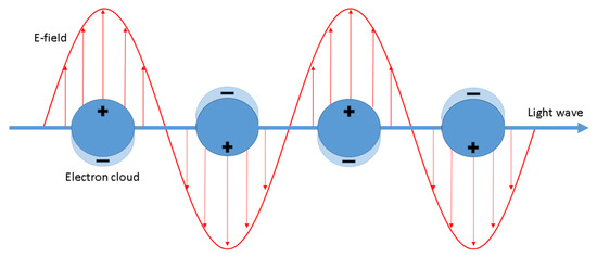
Figure 1.
Schematic illustration of the surface plasmon resonance (SPR) phenomenon. Reproduced with permission [6]. Copyright, 2020, Springer Nature.
The second enhancement mechanism, which also leads to an increase in the efficiency of the generation of the Raman signal, is called the chemical enhancement. The interaction of adsorbed molecules with the metal substrate provides new electronic transitions for metal (or adsorbed molecule) electrons. The electrons at the Fermi level of the metal can be virtually excited into unoccupied molecular orbitals of the adsorbed molecule and back to the metal (see Figure 2a), or the electrons at the highest occupied molecular orbital can be virtually excited into the Fermi level of the metal and back to the adsorbed molecule (see Figure 2b). This means that a mechanism analogous for the standard resonance Raman process (that can generate a significant increase in the efficiency of the generation of the Raman signal) may be observed for adsorbed molecules [7].
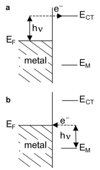
Figure 2.
Schematic illustration of the energy levels involved in the charge transfer (CT) mechanism of the surface-enhanced Raman scattering (SERS) enhancement; hν—photon energy, EF—Fermi level energy, ECT—energies of occupied and unoccupied levels of the adsorbed molecules. (a) The electrons at the Fermi level of the metal are virtually excited into unoccupied molecular orbitals of the adsorbed molecule and back to the metal, (b) the electrons at the highest occupied molecular orbital can be virtually excited into the Fermi level of the metal and back to the adsorbed molecule. Reproduced with permission [7]. Copyright, 2009, Elsevier.
To record the SERS spectrum, Raman scatterers (studied molecules) must be adsorbed at or be placed in a close proximity to the SERS-active material. The first surface-enhanced Raman spectra were published in 1974—in this case, the measurements were carried out on nanostructured silver [6]. During the next three decades, the SERS measurements were also carried out mainly on nanostructured plasmonic metals (Ag, Au and Cu), although other SERS substrates were also developed relatively quickly: in 1982, Loo recorded SERS spectra using as a SERS-active material polycrystalline TiO2 [8] and in 1983, Yamada and Yamamoto produced SERS-active materials by the deposition of some metals on the surface of NiO and TiO2 [9]. The number of SERS measurements carried out on composite substrates containing non-metallic nanostructured materials are still increasing. This is due to many significant advances of such SERS substrates in some applications of SERS spectroscopy, such composites usually have additional important functionalities that are not possible to obtain in standard SERS substrates produced only from plasmonic metals. In this review article, we present selected SERS substrates that utilize nanostructured non-metallic materials, including non-metallic nanostructured thin films or non-metallic nanoparticles covered by plasmonic metals and SERS-active nanomaterials that do not contain plasmonic metals. Some future perspectives of the application of composite SERS substrates are also discussed.
2. Non-Metallic Nanostructured Thin Films Covered by Plasmonic Metals
Nanostructured surfaces of semiconductors or insulators covered with plasmonic metals are very often used as SERS substrates. Few types of such substrates are even available commercially. In many cases, deposition of a plasmonic metal on the nanostructured surface of a semiconductor or an insulator may lead to SERS materials that generate higher and spatially more reproducible SERS enhancement factors than the standard SERS substrates produced from pure gold or silver. Moreover, the cost of the production of such substrates may be lower than the cost of manufacturing standard SERS substrates made from pure gold of silver. In this review, only substrates produced on selected inorganic substrates are described. In particular, we focused on the three most commonly used types of SERS substrates obtained from nanostructured films: TiO2, GaN and ZnO. Such SERS substrates have been extensively studied by many groups, and in this review, we want to show how complex these apparently simple systems are. SERS substrates may be, however, also produced on other nanostructured inorganic films, for example on ZrO2 [10]. Moreover, in addition to SERS materials formed on inorganic substrates, there are also widely used so called paper-based SERS substrates that are formed on cellulose [11,12,13]. This type of SERS substrate is also not described in this work.
2.1. Titanium(IV) Oxide
One of the most used materials with a nanostructured surface, on which a layer of a plasmonic metal is deposited to form SERS substrate, is an ordered film formed from titanium(IV) oxide nanotubes. Titanium can be quite easily covered by the layer formed from titanium(IV) oxide nanotubes by oxidative anodization. This method of synthesis of TiO2 nanotubes allows the obtention of nanostructures with different parameters depending on the electrolyte used [14] and the voltage [15] at which the reaction is carried out. The electrochemically obtained nanotubes are usually annealed for a few hours in order to change the structure of TiO2 from an amorphous one to an anatase or rutile structure [16]. Reconstruction of the crystallographic structure of TiO2 makes the layer of nanotubes on titanium substrate more stable and more mechanically durable.
Pisarek et al. analysed properties of layers of plasmonic metals (Ag, Cu and Au) electrosputtered on previously obtained TiO2 nanotubes [17,18,19,20,21]. In these studies, TiO2 nanotubes were obtained by anodizing a thin titanium foil in an electrolyte containing 47.14% water, 52% glycerin and 0.86% NH4F w/w. The anodization potential significantly influenced the obtained nanotubes—the higher voltage, the larger the internal diameter of the formed nanotubes (see Figure 3) [19].
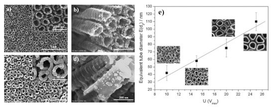
Figure 3.
(a–d) SEM images of a layer of TiO2 nanotubes formed by the anodization of Ti foil in a glycol fluoride solution at 25 V covered by various amounts of Ag: (a,b) 0.01 mg·cm−2, (c,d) 0.06 mg·cm−2. (e) The diagram presenting the dependence between applied anodic voltage and the diameter of formed nanotubes. Reprinted with permission from [19]. Copyright 2010 Elsevier.
The anodization process lasted from about 13 min to 2 h. The anodization time affected the length of formed nanotubes but practically did not affect their diameter. In order to increase the stability of the formed material, the obtained nanotubes were annealed at a temperature of 600 °C for 1 h to 2 h, which led to the transition of the titanium(IV) oxide from amorphous to rutile face. When the annealing is carried out at lower temperatures (400 °C), instead of rutile, the anatase is obtained. In this case, the transition area between the Ti substrate and TiO2 nanotubes is, however, less developed, which leads to lower mechanical stability of the TiO2 layer [18]. The coating of the TiO2 nanotubes by the film of the plasmonic metal may be realized, for example, by the sputter-deposition technique. Table 1 shows how the amount (in mg·cm−2) of silver deposited by sputtering on the layer of TO2 nanotubes influences the structure of the formed film [19].

Table 1.
The correlation between the amount of silver deposited by sputtering on the layer of TO2 nanotubes and the structure of the formed metallic layer.
In addition to the dependence on the mass of deposited metal, the structure of formed plasmonic films depends on the kind of deposited metal (Ag, Au or Cu) and on the diameter of nanotubes on which the deposition is carried out. Although this dependence is relatively complex, some general rules on how the structure of formed film changes upon increasing the amount of the deposited metal may be, however, observed. When small amounts of sputtering metal are deposited, only single small nanoparticles on the surface of nanotubes are observed. Then, after deposition of an additional metal, we can observe the formation of metal rings on the end of nanotubes and the reduction in the diameter of nanotubes. After deposition of an additional portion of metal, the upper surface of the nanotubes becomes completely covered with a metal film. However, at all stages of metal deposition, semi-spherical nanoparticles with a diameter from 5 to 20 nm were visible. In the case of deposition of copper, the formation of the compact metal layer is observed at a significantly earlier stage of sputtering [21]. The formed films were investigated using Auger electron spectroscopy (AES). On the basis of the obtained AES results, it was found that the copper films deposited on the surface of nanotubes are covered with a thin layer of copper oxide. Formation of gold and silver oxides was not observed [21]. In addition, it was found that the MNN Auger signal from silver deposited on the TiO2 substrate was significantly wider than in the case of measurements of Auger spectra of pure silver. This suggests a significant interaction between the deposited silver nanostructures and the TiO2 substrate.
Interactions between deposited metal clusters and the TiO2 substrate do not only influence the structure of the deposited metal clusters. For example, sputtering copper on TiO2 nanotubes leads to a significant broadening of the Raman band at 900 cm−1 corresponding to the Ti=O stretching vibration [20]. Roguska et al. suggested that this broadening is due to the formation of mixed oxides during the sputtering of Cu onto the TiO2 substrate (titanium oxide is mixed with copper ions).
Mao et al. observed that the SERS substrates produced by the deposition of silver on TiO2 nanotubes can self-clean when illuminated with UV radiation [22]. In this case, TiO2 nanotubes were obtained by 15 min anodization of titanium in a glycol solution of HF (0.5% vol) at various voltages (between 20 V and 60 V). Originally formed nanotubes from amorphous TiO2 were heated at 500 °C for 2 h in order to change the structure of TiO2 to anatase. Then, a thin layer of silver (0.03 mg/cm2) was deposited. Mao et al. found that when such systems are stored in humid air, their illumination with UV radiation (with the wavelength of 365 nm) leads to changes in the structure of the deposited silver clusters [22]. One of the effects induced by the UV irradiation is the transfer of silver to the inner parts of the nanotubes. As mentioned above, Mao et al. also noticed that after UV irradiation, the Raman signal from the previously adsorbed organic compound significantly decreases, which means that this substrate has self-cleaning properties.
Silver nanostructures may be deposited on the surface of TiO2 nanotubes not only by the sputtering in vacuum, but also by a chemical reduction of a silver salt, for example, through the polyol process [23]. Meng and Xie found that when silver clusters are deposited using the polyol process, only a few silver nanoparticles were attached to the walls of TiO2 nanotubes, most formed nanoparticles were deposited on the top edges of nanotubes [23]. In the next step, Meng and Xie decided to cover formed TiO2/Ag composite with a layer of graphene oxide (GO). It has been shown that the presence of GO facilitates adsorption of methyl blue on the surface of such material. This is due to the π–π interactions of graphene rings with the rings of methyl blue and due to a significantly developed surface of such composite. The obtained TiO2/Ag/GO composite was tested as a SERS substrate. Meng and Xie found that the intensity of the SERS spectra of methyl blue adsorbed on TiO2/Ag/GO composite is larger than in the case of SERS measurements on the TiO2/Ag composite before covering with GO [23]. The authors believe that the GO layer is so thin that it does not influence the plasmonic interactions, and the aforementioned better adsorption increases the concentration of methyl blue on the surface. After 60 days storage of SERS substrate covered with GO, the decrease in the intensity of the SERS spectrum of methyl blue is only 5%, which is much smaller than in the case of the sample without GO, where the decrease in the intensity of the measured SERS signal is 55%. The authors believe that graphene oxide protects silver nanoparticles from oxidation. Meng and Xie also found that the covering with GO improves the efficiency of self-cleaning of such SERS substrate under the influence of UV radiation. They associate this effect with the possibility of electron transfer and a larger surface area of the GO layer.
It is also possible to attach previously synthesized plasmonic nanoparticles to TiO2 nanotubes [24,25]. In such a case, one can attach a large number of very similar (having practically the same shape and size) plasmonic nanoparticles to the TiO2 nanotubes. For example, Ambroziak et al. immobilized previously synthesized cubic silver nanoparticles on TiO2 nanotubes [25]. Cubic silver nanoparticles have been synthesized using the polyol method developed by Skrabalak et al. [26]. When illuminated by the proper electromagnetic wave, silver cubic nanoparticles generate at their corners and edges a significantly enhanced electric field [27], and hence, the enhancement of the SERS spectrum generated by such plasmonic nanostructures is significantly larger than that generated by the respective spherical plasmonic nanoobjects. Ambroziak et al. found that the SERS enhancement generated by the SERS substrate produced by the attachment of cubic silver nanoparticles to TiO2 nanotubes (when only a part of the outside surface is covered by the plasmonic material) is even higher than the SERS enhancement generated by the standard electrochemically nanostructured solid silver substrate. Moreover, the spatial reproducibility of the SERS enhancement factor for such composite TiO2-nanotubes/cubic-Ag nanoparticles substrate is larger than that for the standard electrochemically nanostructured silver substrate [24].
Sun et al. analysed how the wall thickness of TiO2 nanotubes, on which Ag nanoparticles were deposited, influences the SERS enhancement factor achievable on this material [28]. In other words, the purpose of these studies was to find the wall thickness of TiO2 nanotubes, which allows us to maximize the number of hot spots (places where especially large enhancement of the electric field is generated—hot spots are observed in narrow slits between plasmonic nanostructures or on sharp structures on surfaces of plasmonic objects) created during the silver deposition by e-beam evaporation, and hence, allows the obtention of the SERS substrate generating the highest SERS enhancement factor. Sun et al. found that the optimal wall thickness of TiO2 nanotubes is about 20 nm. The SERS enhancement factor for 2-mercaptobenzoxazole adsorbed on such SERS substrate (with the wall thickness of TiO2 nanotubes equal to 20 nm) is 2.26 × 10⁸. As for other described above TiO2-nanotubes/Ag composites, the obtained SERS substrate is self-cleaning when illuminated with UV radiation. Sun et al. carried out the following experiment three times: 2-mercaptobenzoxazole was adsorbed on the TiO2-nanotubes/Ag composite, the SERS spectrum was measured, then the substrate was irradiated for 20 min using a UV lamp and was rinsed with water. The spectrum of the “cleaned substrate” was measured again. It was found that after UV irradiation, the SERS spectrum of 2-mercaptobenzoxazole disappeared, and after reapplying this compound to the SERS substrate, practically identical SERS spectra were obtained.
2.2. Gallium Nitride
Another often used surface-nanostructured material, on which a layer of a plasmonic metal can be deposited to form an efficient SERS substrate, is porous gallium nitride. In 2005, Bohn et al. published a paper showing that the surface-nanostructured GaN coated with gold and silver is very efficient SERS substrate [29]. After the cleaning process (in principle successive immersion in the following solvents: acetone, 2-propanol, 65% HNO3, water and methanol), GaN substrates were placed in an etching solution of CH3OH, HF (49%) and H2O2 (30%) in 1:2:2 volume ratio and illuminated for 90 min with UV radiation. This made the surface of the GaN sample very porous. Subsequently, the etched surface of GaN was cleaned by washing with water and methanol and then sonicated for 15 min to remove ridge structures. The resulting porous structure formed on the etched surface of GaN resembles nanotubes. Then, a layer of gold and silver was deposited. Deposition of the layer of plasmonic metal can be realized by the vacuum evaporation or by the chemical reduction of a silver or gold compound. In the case of the chemical coating, before the deposition of the plasmonic film, the nanostructured GaN substrates were immersed in concentrated HF to remove surface oxides. Plating with gold was performed using a three-step method containing: sensitization, activation, and platting. The sensitization was performed by placing the etched GaN substrate in water–methanol diluted solution of SnCl2 and CF3COOH. Activation was performed by the immersion of the GaN substrate in a mixture of a solution of AgNO3 and aqua ammonia. The plating step was performed by the immersion of the GaN substrate in a mixture of diluted commercially available Au plating solution and NaHCO3 and Na2SO3. Then, the formaldehyde was added as a reducing agent. After the deposition of the gold film, the substrates were rinsed with water and with 25% HNO3. The silver films were obtained by a similar method; the only difference was that in this case the plating solution was identical to the activation solution (see above)—immediately prior to silver deposition, formaldehyde was added to the plating solution to act as a reducing agent. Gold and silver films deposited using the described above chemical methods were composed mainly from many spheroidal nanostructures. Silver and gold films have been also deposited on the nanostructured GaN substrates by thermal evaporation. In this case, formed films were significantly flatter. The SERS enhancement factors generated by the formed SERS substrates were determined using malachite green isothiocyanate as a Raman scatterer. In the case of nanostructured GaN substrates covered with the gold layer, the SERS enhancement factor determined for the sample with the chemically deposited layer was equal to 2 × 10⁴, whereas for the sample with the evaporated gold layer the SERS enhancement factor was equal to 2 × 10⁵. In the case of samples with a silver film, a larger SERS enhancement factor (equal to 1 × 10⁸) was obtained on the substrate covered using the chemical process than on the substrate covered by the vacuum evaporation (5 × 10⁷) [29].
Many materials for SERS measurements based on nanostructured GaN substrates containing the surface nanopillars shaped-like conical sheaves have been produced by Weyher et al. (example morphologies of studied materials are shown in Figure 4). On such surface-nanostructured GaN substrates, gold [30,31,32,33], gold and silver alloy [34] or gold and copper alloy [35] were deposited. In this case, the nanostructuring of GaN surface was realized by pre-etching in a 10% HF solution and subsequent photo-etching using a 300 W xenon UV lamp in a solution of 0.02 M KOH and 0.02 M K2S2O8. Then, pure plasmonic metals or their alloys were electrosputtered onto nanostructured GaN substrate. The obtained morphology of the nanostructured GaN surface allows the obtention of SERS substrates with a significant number of hot spots. For example, after the deposition of the gold layer with a thickness of 90 nm [32], the SERS enhancement factor for the obtained SERS substrate was determined as equal to 2 × 10⁶ (as a Raman scatterer p-mercaptobenzoic acid was used). The SERS spectrum measured using this substrate has very high reproducibility—relative standard deviation of the intensity of the spectra measured at various sites was only 10%. Produced GaN/Au SERS substrate was also very stable over time, after 10 months, the intensity of the measured SERS spectrum decreased by only 10% compared to the freshly made substrate. Weyher et al. also studied the influence of the annealing at various temperatures of the GaN/Au substrates on their structure and their SERS activity [36]. Annealing up to the temperature of 200 °C increases the SERS enhancement factor, which is attributed to the generation of more hot spots. Annealing in the temperatures between 250 and 350 °C decreases the intensity of the measured SERS spectrum due to the coalescence of nanoparticles. Increase in the intensity of the measured SERS spectrum is observed again for GaN/Au substrates annealed in the temperatures between 450 and 750 °C, which is associated with the formation of crystallographic planes enabling surface binding sites and forming SERS hot spots.
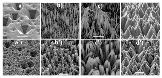
Figure 4.
SEM images of GaN samples after: (a) orthodox etching at 420 °C for 10 min, (b,c) galvanic photo-etching for 8 and 12 min, respectively, (d) electroless photoetching for 120 min. (a’–d’) shows SEM images of similar samples after sputtering of an Au-Ag alloy. The samples are tilted 45°. The scale bars represent 1 μm. Reprinted with permission from [37]. Copyright 2018 Elsevier.
As mentioned above, nanostructured GaN substrates with nanopillars shaped-like conical sheaves on the surface have been also covered with some alloys of gold. Using gold alloys instead of the pure gold allows the modification of the plasmonic properties of the deposited film and also allows to easily increase the roughness of the film by dealloying. For example, GaN substrates covered with Au:Ag alloy (initially 70/30 wt%) after soaking for one day in nitric(V) acid become (due to the dealloying the content of silver drops to 19%) significantly more rough and more SERS-active. The SERS enhancement factor generated by this substrate in measurements with p-mercaptobenzoic acid was estimated as equal to 1.5 × 10⁷ [34]. The dealloyed Au/Ag film is chemically very resistant, for example, the content of silver does not change significantly even after further long soaking in nitric(V) acid. This means that the obtained substrate combines the high chemical stability of gold and the significantly better plasmonic properties of silver. In another experiment, such type of nanostructured GaN substrates have been covered by AuCu alloy (40/60 at%) [34]. Again, after dealloying in nitric acid, the Cu content drops to 10% and the SERS enhancement factor achieves the value of 2 × 10⁵.
The surface of GaN can be also nanostructured in another manner. For example, Weyher et al. at first etched the surface of GaN in a molten eutectic KOH—NaOH mixture, which led to the creation of inverted pyramids on the surface of the GaN substrate, and then the previously described process of the creation of nanopillars shaped-like conical sheaves was realized [35,37]. In the next steps, AuCu alloy (40/60 at%) [35] or AuAg alloy (70/30 at%) [37] were deposited and the obtained films were further etched in nitric acid. Weyher et al. found that the initial nanostructuring leading to the creation of the inverted pyramids induced an additional increase in the SERS enhancement factor, for example, in the case of experiments with AgCu alloy, to 5 × 10⁵ (as mentioned above, the SERS substrate produced without the step of the creation of the inverted pyramids on the GaN surface generates the SERS enhancement factor equal to 2 × 10⁵ [35]. Figure 5 shows example SERS-activity maps for various GaN samples covered with AuAg alloy [37].
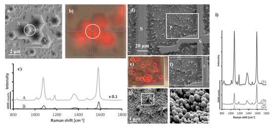
Figure 5.
(a,b) SEM images and corresponding SERS intensity map of the spectrum of p–mercaptobenzoic acid adsorbed on the surface of GaN/AuAg (plot represents intensity of the band at 1590 cm−1), (c) recorded SERS spectra of p–mercaptobenzoic from A: point indicated by white circle on (a) and B: point indicated as Y. (d,f–h) SEM images of photo-etched GaN samples, (e) SERS intensity map of the band at 1590 cm−1 of p–mercaptobenzoic acid and (i) SERS spectra of p–mercaptobenzoic acid recorded on substrates having various GAN morphologies: 1 nano-pillars, 2 on the matrix, 3 at the position matched as X in (a). Reprinted with permission from [37]. Copyright 2018 Elsevier.
An interesting method of preparation of nanostructured GaN films has been proposed by Shivaprasad et al. [38]. This group prepared a sponge-like GaN network through the plasma assisted molecular beam epitaxy. The change of the parameters of the epitaxial growth allows the preparation of various sponge-like GaN networks, for example, with the average wall thickness of 40 nm or much more densely packed structures with the wall thickness of 60 nm (see Figure 6). Then, on such nanostructured GaN substrates, silver was deposited using electron beam evaporation. The SERS enhancement factor after deposition of the amount of silver required to form the silver film with the average thickness of 13 nm was estimated as equal, on average, to about 105—differently prepared substrates generate slightly different SERS enhancement factors. In general, higher SERS enhancement factors were observed on more densely packed GaN nanostructures, which is probably related to the larger number of hot spots created in this system.
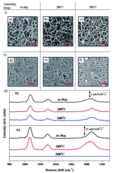
Figure 6.
SEM images of GaN nanowalls covered with silver: less densely packed (S1) and more densely packed (S2). (a,d) Without annealing, (b,e) after annealing at 200 °C, (c,f) after annealing at 500 °C. (g) SERS spectra for substrates S1 and S2. Thiophenol was used as a test molecule. Reprinted with permission from [38]. Copyright 2015 Royal Society of Chemistry.
2.3. Zinc Oxide
Efficient SERS substrates are also often produced utilizing the nanostructured film of zinc oxide. For example, in 2010, Ozaki et al. synthesized a very efficient SERS substrate by the deposition of a thin layer of silver on the film of zinc oxide nanorods [39]. Zinc oxide nanorods with hexagonal arrangement were obtained by hydrothermal synthesis. At first, a zinc foil cleaned in water and alcohol was placed in an autoclave filled with an aqueous solution of 0.9 M NaCl and 5.56 mM acetic acid. The temperature was raised to 120 °C and the zinc foil was kept for 14 h at this temperature. This led to the formation of ZnO nanowires on the surface of the foil, with a diameter between 200 and 500 nm and the length of about 2 μm. Then, the deposition of silver nanostructures was carried out by the immersion of the Zn/ZnO sample in AgNO3 solution. Ozaki et al. found that the Ag nanostructures were only formed at the top of the nanorods, which is probably caused by the mechanism of the transfer of the electric charge from the Zn substrate only along the ZnO nanorods. Changing the time of silver deposition and the concentration of the AgNO3 solution, it is possible to control the size and density of the formed Ag nanoparticles. For example, when the ZnO substrate was immersed in 10−5 M AgNO3 solution for 1 min, only a few small nanoparticles with a size between 10 and 20 nm are formed at the top of ZnO nanorods. With the increase in the concentration of AgNO3 solution, larger Ag nanoparticles are formed. Ozaki et al. found that the highest SERS enhancement factors (ca.·106) were measured using the substrates obtained by the immersion of ZnO substrates for 1 min in a AgNO3 solution with the concentration in the range between 10−4 and 10−3 M [39].
An interesting SERS substrate containing nanostructured ZnO was developed by Fan et al. [40]. At first, a nanopillar Si array was achieved using standard top-down photolithography pattering followed by dry etching and wet etching to remove metal and oxides. The obtained Si nanopillars were 300 nm high, 150 nm in diameter and the distance between them was about 400 nm. ZnO seeds needed for the branch growth were obtained via the atomic layer deposition using diethyl zinc and water. Then, the prepared substrate was putted into Zn(NO3)2 and hexmethylenetetramine solution and kept at 95 °C for 3 h. This process led to the formation of ZnO branches that were perpendicularly directed to the Si nanopillars, were 150–200 nm long and about 30 nm in diameter (see Figure 7). Finally, the silver was deposited by the photochemical method: the substrate was placed in a 0.1 M AgNO3 solution for 20 min and then was illuminated for 3 min using a 25 W UV lamp. The silver nanoparticles formed on the ZnO branches had a diameter of about 20–30 nm. Fan et al. determined the SERS enhancement factor for this system as equal to 106 [40].
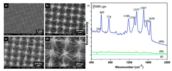
Figure 7.
(a–d) SEM images of the ordered Si/ZnO nanotrees: (a,b) top view, (c,d) 20o titled view, (e) SERS spectra of molecules of rhodamine 6G adsorbed from the solution with the concentration of 10−6 M collected from: (I) Si/ZnO nanotrees, (II) Ag nanoparticles substrate prepared by the sputtering method, (III) Si/ZnO nanotrees decorated by Ag nanoparticles. Reprinted with permission from [40]. Copyright 2010 American Chemical Society.
Additionally, ZnO nanoneedles covered with silver nanoparticles can be used as SERS substrates [41]. ZnO nanoneedles were formed by the immersion for 12 h of a cleaned zinc foil in a 0.5 M Zn(NO3)2 and 3 M KOH solution. The sample prepared in this way was rinsed with water and dried. Obtained ZnO nanoneedles were perpendicularly oriented to the metal substrate and have a diameter of 6–10 nm. Silver nanostructures on a ZnO substrate were obtained by the immersion of the nanostructured ZnO substrate in 10−3 M AgNO3 solution and exposing it to the sun radiation for 20 min. This leads to the formation of monocrystalline silver nanoparticles with a diameter of 10 nm, which were attached to the surface and tips of ZnO nanoneedles (see Figure 8). Wang et al. showed that such SERS substrates may be used to detect Sudan II and Sudan IV dyes at concentrations as low as 10−12 M [41].
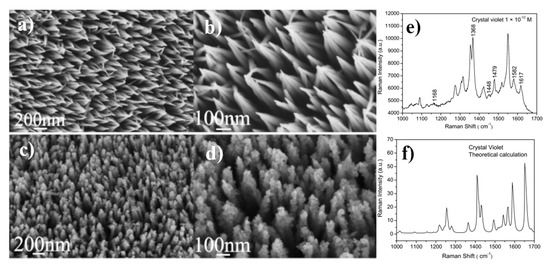
Figure 8.
(a,b) SEM images of ZnO nanoarrays; (c,d) SEM images of ZnO/Ag composite nanoarrays, (e) SERS spectrum of crystal violet adsorbed on ZnO/Ag composite nanoarrays from 10−12 M crystal violet solution, (f) theoretically calculated Raman spectrum of crystal violet. Reprinted with permission from [41]. Copyright 2011 Elsevier.
Highly SERS-active material may be also obtained by the deposition of gold nanoparticles on the nanostructured ZnO. For example, Lee et al. produced SERS substrates by the deposition of gold nanoparticles on ZnO nanorods and nanoneedles (see Figure 9) [42]. ZnO nanoneedle and nanorod arrays were grown on an aluminium-doped zinc oxide by chemical vapor deposition. Then, the nanostructured ZnO substrates were immersed in water–methanol solution of HAuCl4 (the concentration of Au ions was in the range between 0.1 and 0.5 mM), the sample was placed in an autoclave and kept at 120 °C for an hour. The amount of the deposited gold on the surface of ZnO nanoneedles can be controlled by altering the concentration of HAuCl4. When the amount of the deposited gold is high, ZnO/Au nanoneedles form bundles. The obtained substrates were tested for the enhancement of the Raman spectrum using rhodamine 6G. The highest achieved enhancement factor was 1.2 × 10⁷ [42].
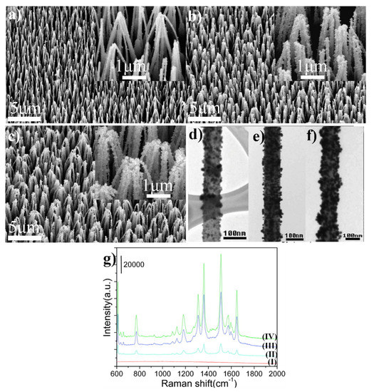
Figure 9.
(a–c) SEM images of ZnO/Au nanoneedle arrays prepared at different HAuCl4 concentrations: (a) 0.1, (b) 0.3 and (c) 0.5 mM. Inset shows corresponding high magnification SEM images. (d–f) TEM images of ZnO/Au nanoneedles prepared at different HAuCl4 concentrations: (d) 0.1, (e) 0.3 and (f) 0.5 mM. (g) SERS spectra of molecules of rhodamine 6G adsorbed on: (I) ZnO (II), (III) and (IV) ZnO/Au produced using HAuCl4 at various concentrations: 0.1, 0.3 and 0.5 mM, respectively. Reprinted with permission from [42]. Copyright 2009 American Chemical Society.
Alessandri et al. showed that the SERS substrates produced by the sputtering of gold on ZnO nanorods have self-cleaning properties [43]. In order to obtain the ZnO nanorods, at first, ZnO islands on Si wafers were formed by atomic layer deposition. The production of ZnO islands on Si wafers allows the control of the distribution of sites of future ZnO growth. Then, the growth of ZnO nanorods was carried out by the hydrothermal method, in short: the Si wafer with ZnO seeds was placed in an aqueous solution of 0.02 M Zn(NO3)2 and 0.04 M hexamethylenetetramine and was kept at 90 °C for 6 h. The produced nanorods were between 300 and 400 nm in length and their diameter was about 30–40 nm. On the obtained ZnO nanorods, gold was sputter deposited at room temperature. The obtained material was tested as a substrate for SERS measurements: it was found that it is possible to record the SERS spectrum of methylene blue even at the concentration of 10−12 M. Additionally, the self-cleaning properties of the substrate have been demonstrated. After the recording of the SERS spectrum of methylene blue adsorbed from the solution with a concentration of 10−4 M, the substrate was irradiated with a UV lamp. It was shown that after 15 min of irradiation, the SERS signal became very weak, and after 30 min of exposure, the characteristic SERS spectrum of methylene blue completely disappeared.
3. Non-Metallic Nanoparticles Covered by Plasmonic Metals
To produce effective SERS substrates, plasmonic metals are deposited not only on the macroscopic nanostructured non-metallic materials, but sometimes plasmonic metals are also attached to some non-metallic nanoparticles. Although SERS substrates formed on non-metallic nanoparticles are not used as often as materials for SERS measurements formed on macroscopic nanostructured materials (some types of macroscopic SERS substrates, for example, formed on nanostructured macroscopic GaN are even commercially available), there are also many important types of SERS substrates that have the form of such nanocomposites. In this section, we describe three selected examples of the most important substrates produced by combining metallic and non-metallic nanostructures that have some additional functionalities in comparison to the SERS substrates formed only from plasmonic metals.
3.1. Iron Oxides
Probably the most important type of SERS materials obtained from the nanostructured non-metallic nanoparticles and the plasmonic metals are magnetic SERS substrates. Introducing the additional functionality (magnetism) to the SERS substrates significantly facilitates the deposition of such materials and their removal after the measurement—these processes may be easily carried out with an inexpensive commercially available neodymium magnet. For example, very often plasmonic nanoparticles used as SERS substrates are deposited on an analysed surface by the deposition of a drop of their sol and evaporation of the solvent. Unfortunately, when this simple method of deposition is used, due to the so-called coffee ring effect, a significant accumulation of nanoparticles at the boundary of the area covered by the sol is usually observed. When the deposited nanostructures also have magnetic properties, and the deposition is carried out in the magnetic field (for example, generated by a strong magnet), the coffee ring effect is usually eliminated, and homogeneously distributed films of nanostructures are formed. SERS magnetic–plasmonic substrates may be also relatively easy removed from the analysed sample using a strong magnet. Therefore, many groups are working on the development of SERS substrates with magnetic properties. For example, Sun et al. synthesized Fe3O4@AuAg alloy core–shell nanoparticles [44]. At first, Fe3O4 nanoparticles were synthesized by solvothermal reaction; briefly: a solution of FeCl3·6H2O, sodium citrate and sodium acetate in ethylene glycol was heated at 200 °C for 10 h. Then, Fe3O4 nanoparticles were functionalized with NH2-terminated silane coupling reagent (3-aminopropyltrimethoxysilane), the sol of functionalised Fe3O4 nanoparticles was mixed with a sol of small Au nanoparticles and the obtained mixture was sonicated, which led to the formation of Fe3O4-Au composites. In the second stage, the obtained Fe3O4-Au composites were kept in an Au-Ag alloy shell growth solution (which contained: HAuCl4, AgNO3, K2CO3, NH3, and HCHO). By changing the amount of HAuCl4 and AgNO3, the Fe3O4@AuAg alloy nanoparticles with different component ratios of Au and Ag were prepared. Changing the molar fraction of Ag and Au led to a significant change in the plasmon properties of the obtained structures.
As mentioned above, many other types of magnetic SERS materials have been synthesized, for example: agglomerates of gold and carbon-covered Fe3O4 nanoparticles [45], silver nanoflowers formed on the surface of core–shell Fe3O4@Au nanoparticles [46] or even four-layer Fe3O4@Ag@SiO2@Au microspheres [47]. Attaching a plasmonic nanostructure to the magnetic part of the composite need not cause a significant reduction in the SERS activity of the obtained SERS substrate, for example, the SERS enhancement factor achievable on silver nanoflowers formed on the surface of core–shell Fe3O4@Au nanoparticles was estimated to be equal to 2.2 × 10⁹ [46].
An interesting universal method of producing of magnetic SERS substrates has been proposed by Kolataj et al. [48]. This group found that various metallic nanoparticles easily bond to the surface of magnetic γ–Fe2O3 nanoparticles functionalized with (3-aminopropyl)trimethoxysilane. Kolataj et al. showed that when this method of formation of agglomerates is used, the initial size and shape of the noble metal nanoparticles do not change during the process of linking; therefore, highly anisotropic plasmonic structures may be attached to the magnetic nanoparticles. Kolataj et al. also emphasized that such composites form homogeneous layers in the magnetic field, so reproducible SERS substrates may be easily formed using this material [48].
3.2. Molybdenum Oxides
The other important type of SERS materials obtained from the nanostructured non-metallic nanoparticles and the plasmonic metals are nanoparticles of molybdenum oxide on which a plasmonic metal has been deposited. These type of SERS substrates are very promising because, as described in detail in the next section, nanostructured molybdenum oxides (both MoO2 and MoO3) are very active in SERS spectroscopy, and the SERS enhancement factor generated by nanostructured MoO2, MoO3−x or MoO3 may even reach the values generated by standard silver and gold SERS substrates. Combining molybdenum oxide and metallic plasmonic nanostructures gives SERS substrates for which both electromagnetic and chemical enhancements are very large—so an interesting synergistic enhancement effect is observed [49]. An example of such a substrate was formed by Shi et al., who synthesized MoO3@Ag hybrid nanostructures. This group separately synthesized MoO3 nanowires (using the hydrothermal method, briefly: aqueous solution of ammonium molybdate and nitric acid was heated at 180 °C for 12 h using a Teflon-lined stainless autoclave), silver nanoparticles and then self-assembly of Ag nanoparticles on the surface of MoO3 nanowires was carried out using (3-aminopropyl)diethoxy methylsilane as a coupling agent [49].
Effective combination of the electromagnetic and chemical SERS enhancements has been also reported for nanostructured molybdenum oxides decorated with gold nanoparticles [50]. Although, as mentioned above, nanostructured molybdenum oxides are already an effective SERS substrate, the deposition of gold nanoparticles leads to a further increase in the SERS enhancement factor generated by this material (in this case, by a factor of eight).
3.3. Titanium(IV) Oxide
An interesting functionality that can be achieved by SERS substrates due to the attachment of another material to the plasmonic nanoparticles is self-cleaning under UV irradiation. For example, Shen et al. formed multifunctional Fe3O4@TiO2@Ag-Au microspheres (see Figure 10), which were efficient SERS substrates with strong magnetic properties and, due to the presence of a TiO2 layer, also have self-cleaning properties [51]. Shen et al. found that this material reveals some catalytic properties, for example, it may be used as a catalyst in the reduction of 4-nitrophenol to 4-aminophenol. This means that this three-layer core–shell Fe3O4@TiO2@Ag-Au composite shows great potential as a multifunctional platform for simultaneous catalysis and in-situ reaction monitoring.
Figure 10.
(a) The simulation model of Fe3O4@TiO2@Ag and (b) Fe3O4@TiO2@AuAg nanoparticles, (c) the calculated electromagnetic field distribution around Fe3O4@TiO2@Ag and (d) Fe3O4@TiO2@AuAg nanoparticles. The incident light wavelength was 785 nm. (e) SEM images of Fe3O4 spheres, (f) TEM image of Fe3O4@TiO2 core–shell sphere, (g) SEM images of Fe3O4@TiO2@Ag sphere, (h–j) SEM images of Fe3O4@TiO2@AuAg nanospheres with various molar ratio of Ag:Au: (h) 1:2, (i) 1:1, (j) 2:1, (k–m) the corresponding TEM images, (n) SERS spectra illustrating the reduction of 4-nitrophenol to 4-aminophenol catalysed by Fe3O4@TiO2@Au-Ag nanospheres. Reprinted with permission from [51]. Copyright 2016 Elsevier.
Another material that, in addition to the possibility of generating strong SERS signal, can be used for photocatalysis and photovoltaic applications are anatase TiO2 nanospheres covered with gold nanoparticles [52]. Damato et al. synthetized such a system attaching gold nanoparticles to well-defined (with a diameter of ca. 230 nm) TiO2 nanospheres that have been obtained by the hydrolysis of spheres formed from titanium glycolate.
4. SERS Substrates That Do Not Contain Nanostructured Metals
As mentioned in the introduction, around illuminated nanoobjects formed from plasmonic metals (e.g., Au, Ag or Cu), a very large enhancement of the intensity of the electric field may be observed, which leads to very large increase in the efficiency of the generation of Raman signal by molecules placed in such places. Therefore, typically used SERS substrates contain nanostructured plasmonic metals, and, for such substrates, the total SERS enhancement is dominated by the electromagnetic part. There are also, however, SERS substrates that do not contain any metallic parts, and, in the case of SERS measurements carried out on such substrates, the SERS enhancement is often dominated by the chemical mechanism. Below some typical SERS substrates that do not contain nanostructured metals are presented. As such substrates are often used to study the interaction with the surface of the material from which the substrate is produced, a large number of various materials were nanostructured to record SERS spectrum. Below we present selected examples of SERS-active materials that we consider as the most interesting.
4.1. Titanium(IV) Oxide
Titanium(IV) oxide was the first non-metallic material on which SERS spectrum was observed. In 1982, Loo presented the SERS spectrum of I2 adsorbed on the surface of polycrystalline TiO2 [8]. In this case, polycrystalline TiO2 was prepared by heating a titanium foil in a Bunsen burner to redness for about 1 min. TiO2 seems to be very important material from which SERS substrates are formed, and therefore, the presentation of non-metallic SERS substrates is started from substrates made from TiO2.
Interesting SERS substrates formed from TiO2 have been produced by Qi et al. [53]. At first, this group deposited on a glass slide an agglomerate of polystyrene nanospheres and evaporated the solvent. Then, to the agglomerate of polystyrene nanospheres, the solution of titanium isopropoxide was applied by spincoating. The prepared substrate was dried at 75 °C for 24 h and then heated at the temperature of 450 °C for 2 h. In this way, polystyrene particles were removed and the sponge anatase structure of TiO2 was formed, which was described by the authors as an inverse opal photonic microarray (see Figure 11). The band gap of this material depends on the size of the pores, and their size depends on the particle size of the polystyrene nanospheres used. It was noticed that if the photonic band gap corresponds to the energy of the excitation photons used for the SERS measurements, the recorded SERS spectra are the most enhanced (the achieved SERS enhancement factor was estimated as equal to 2 × 10⁴) [53]. In addition, this SERS TiO2 substrate, similar to many other anatase substrates, has self-cleaning properties under the influence of the sunlight, for example, this opal TiO2 substrate can decompose adsorbed methylene blue after 10 min irradiation with solar light [53].
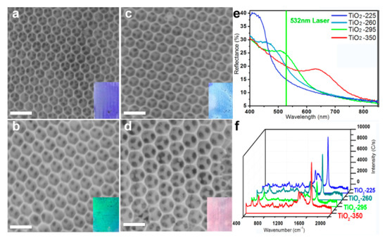
Figure 11.
(a–d) SEM images of TiO2 inverse opal substrates calcined in various temperatures: (a) 225, (b) 260, (c) 295, (d) 350 °C. (e) Reflection spectra of TiO2 inverse opal substrates. (f) SERS spectra of methylene blue adsorbed from 10−5 M aqueous solution on various inverse opal substrates. Reprinted with permission from [53]. Copyright 2014 American Chemical Society.
Yang et al. investigated how the crystallographic structure of the TiO2 nanoparticles (anatase, rutile or a mixture of both phases) influences the SERS enhancement factor generated by such systems [54]. At first, they synthesized TiO2 nanoparticles by the sol-hydrothermal method. Briefly, tetrabutyl titanate dissolved in anhydrous ethanol was added to the mixture of ethanol, water, and nitric acid. Subsequently, the obtained yellowish transparent sol was kept at 160 °C for 6 h in a stainless-steel vessel. Finally, the product was calcined at six different temperatures. The temperature of calcination affects the crystal phase of the obtained TiO2 nanoparticles. In the case of low calcination temperature (400 and 450 °C), the synthesized nanoparticles exhibit pure anatase phase. The samples calcined in high temperature (650 °C) were completely converted into rutile phase. The product calcined between 450 and 650 °C contains both phases. Yang et al. found that the TiO2 nanoparticles with various phase compositions generate various SERS enhancement factors. In the case of the measurement of the SERS spectra of 4-mercaptobenzoic acid adsorbed on the obtained TiO2 nanoparticles, the highest Raman signal is observed when the ratio of the anatase and rutile phase is approximately 85% and 15%. The TiO2 nanoparticles containing both crystal phases generate larger chemical SERS enhancement probably because the separation of the photogenic charge carriers is easier in the mixture of two phases [54].
In addition to the influence of the phase composition of the TiO2 nanoparticles on their SERS activity, defects introduced to the crystal structure of the TiO2 nanoparticles (by doping) may also influence the generated SERS enhancement factor. Xue et al. synthetized TiO2 and Mn-doped (1%, 3% and 5%) TiO2 nanoparticles by a sol-hydrothermal method [55]. Obtained nanoparticles have been tested as substrates for SERS measurements using 4-mercaptobenzoic acid as a Raman scatterer. Xue et al. found that doping of the nanoparticles increases the intensity of the measured Raman signal—the highest SERS signals (by a factor of six higher than the SERS signal measured on pure TiO2 nanoparticles) were observed on the Mn–TiO2 (3%) samples. Xue et al. suggested that an appropriate amount of Mn dopant enriches the surface states and improves the efficiency of photo-generated carrier separation, which leads to the increase in the efficiency of the TiO2-to-molecule charge-transfer process and hence, enhances the SERS intensity due to the increase in the chemical enhancement [55]. A similar effect was observed for TiO2 nanoparticles doped with Zn [56]. The obtained material exhibited the same crystal structure as TiO2 nanoparticles doped with Mn. Similar to TiO2 Mn-doped nanoparticles, the highest SERS signal is observed for Zn loading equal to ca. 3%.
4.2. Silver Halides
The second (after TiO2) non-metallic substrate used for SERS experiments (already in 1984) was a sol of silver chloride [57]. Slightly later (in 1986), the same group showed that also a colloid of silver bromide may be used as a SERS substrate [58]. For these substrates, the enhancement of the recorded SERS spectra was not high, typically one order of magnitude. Although a very simple method of preparation of SERS-active colloids of silver halides; typically, such colloids are formed just by mixing of silver salt with halide salt, after an initial significant interest in this type of SERS substrate, for example see: AgCl [59,60], AgBr [58,61,62] or AgI [63], this type of SERS substrate is not currently in wide use. Some interesting SERS substrates made from silver halides are, however, still being developed. For example, in 2012, Dang and co-workers synthesized SERS-active cubic AgCl nanocrystals by a laser ablation—see Figure 12 [64]. Recently (in 2019), Joo et al. synthesized SERS-active highly monodisperse AgCl nanospheres and nanocubes using a rapid one-pot room-temperature aqueous synthesis [65].
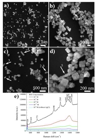
Figure 12.
(a–d) SEM images of the AgCl nanoparticles produced by laser ablation, (e) SERS spectra of molecules of rhodamine 6G on AgCl nanoparticles adsorbed from solutions with various concentrations. Reprinted with permission from [64]. Copyright 2012 Elsevier.
4.3. Copper Oxides
An important group of SERS substrates that do not contain nanostructured metals are nanoparticles of copper oxides. The first report concerning SERS activity of nanostructured Cu2O was published in 1998 by Kudelski et al. [66] (it was the second reported in the literature of SERS-active oxide of a metal that is standardly used to create SERS substrates, the first kind of this type of SERS substrates was colloidal silver oxide [67]). Various Cu2O microcrystals have been tested as SERS substrates by Lin et al., who synthesized highly uniform cubic, rhombic dodecahedral, and octahedral Cu2O microcrystals with well-defined {100}, {110}, and {111} facets and clear surface atomic configuration. Cu2O {100}-cubic nanoparticles were synthesized by the reduction of the alkalized (by the addition of NaOH) solution of CuCl2 by the solution of ascorbic acid. Then, {111}-octahedral Cu2O nanoparticles were obtained using similar procedure; however, a significant amount of polyvinylpyrrolidone was added to the solution of CuCl2. Then, {110}-dodecahedral Cu2O nanoparticles were synthesized by the reduction by D-(+)-glucose of the solution obtained by mixing solutions of CuSO4 and NaOH and oleic acid and ethanol. As one can expect, the interaction of adsorbed molecules with surfaces of the adsorbent with different orientations leads to various complexes, for which different SERS enhancement factors are observed [68]. Lin et al. found that the ratio of SERS enhancement factors for 4-nitrobenzenethiol adsorbed on {100}, {110}, and {111} facets of Cu2O microcrystals is about 15:6:2 [68]. These clearly demonstrate that regarding the SERS measurements on semiconductor substrates, choosing nanoobjects with the proper crystallographic orientation of the outermost surfaces is very important.
It is well known that aggregates (superstructures) formed from plasmonic nanoparticles generate significantly stronger SERS signals than isolated nanoparticles [5]. This is due to the coupling of plasmons induced in the individual plasmonic nanostructures, which generate a very strong electric field in slits between nanoparticles [5]. Lin et al. found a similar effect in clusters of Cu2O nanoparticles, a significantly increased SERS enhancement factor in comparison to the individual nanoparticles, which was explained by the resonance coupling between charge-transfer complexes formed from Cu2O and the adsorbed molecules. Cu2O superstructures studied Lin et al. were cube-like, with a size of about 2 μm and were formed from Cu2O mesoporous spheres with a diameter of ca. 300 nm. SERS enhancement factor generated by these super-structures of Cu2O nanoparticles was comparative to the enhancement factor generated by standard plasmonic SERS substrates and was estimated as 8 × 10⁵ [69].
4.4. Molybdenum Oxides
Very large SERS enhancement factors (even reaching the values generated by standard silver and gold SERS substrates) may be also obtained on nanostructured molybdenum dioxide. For example, Zhang et al. synthesized MoO2 nanoparticles by a simple hydrothermal method, briefly: water and ethanol solution of molybdenyl acetylacetonate was kept (in autoclave) at 180 °C for 20 h—see Figure 13 [70]. Formed MoO2 nanoparticles exhibit plasmonic properties. Obtained material is very stable chemically; the plasmonic band does not change neither its shape nor the position even after contact with many corrosive substances or after heating in air at 300 °C for 24 h. The SERS enhancement factor generated by this substrate was estimated as equal to 3.75 × 10⁶. In the next contribution, this group slightly modified the experimental conditions of the synthesis of MoO2 nanoparticles (isopropanol was added to the reaction mixture), obtaining significantly more regular nanoparticles with the average diameter of about 40 nm, which generated a slightly higher SERS enhancement factor (ca. 4.8 × 10⁶) [71].
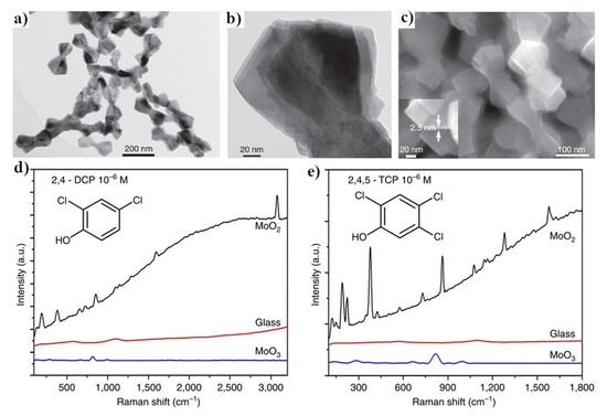
Figure 13.
(a,b) TEM images of the MoO2 nanocrystals, (c) SEM image of the MoO2 nanocrystals, (d,e) SERS spectra of polychlorinated phenols adsorbed on the surface of MoO2. Reprinted with permission from [70].
Chen et al. attached MoO2 nanoparticles to the surface of graphene oxide by a simple hydrothermal procedure [72]. This allowed the obtention of a very active SERS material, which generates a SERS enhancement factor estimated as equal to ca. 1.05 × 10⁷. Formed SERS substrate exhibits very good time stability, the SERS signal decreases only by 4.4% after 40 days. Additionally, in the case of experiments with some organic dyes, graphene oxide significantly reduced in the recorded SERS spectra of the fluorescence background usually generated by molecules of dyes.
Further increase in the SERS enhancement factor generated by MoO2 nanoparticles was obtained by the formation of hollow MoO2 nanostructures. Zhang et al. synthesized hollow MoO2 spheres by the self-assembly of MoO2 nanocones—see Figure 14 [73]. The initial MoO2 nanocones (with a length in the range of 40 and 100 nm and a diameter of ca. 20 nm) were synthesized by anodizing the molybdenum bar in methanol and toluene in the presence of tetramethylammonium bromide as surfactant. Then, the sol of MoO2 nanocones was kept in an autoclave at 260 °C for 24 h, which lead to the arrangement of MoO2 nanocones in spheres (with the size in the range of 500 nm—3 μm). Zhang et al. determined the SERS enhancement factor generated by this system as equal to 3 × 10⁷ [73].
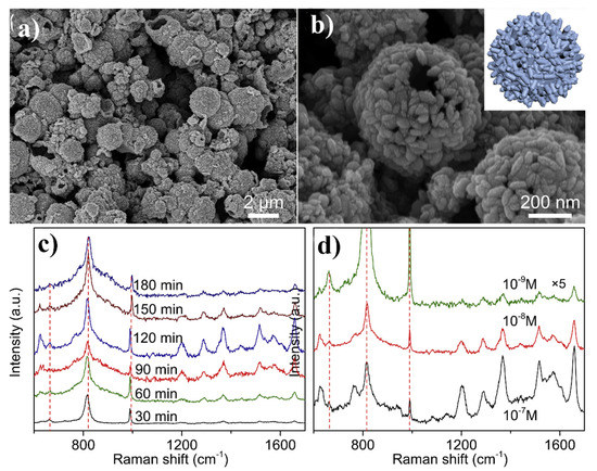
Figure 14.
(a,b) SEM images of hollow MoO2 spheres, inset shows the schematic structure of this nanomaterial, (c) SERS spectra of rhodamine 6G adsorbed on the hollow MoO2 nanospheres after various anodization times from 10–7 M rhodamine 6G solution, (d) SERS spectra of rhodamine 6G adsorbed from solutions with different concentrations on the hollow MoO2 nanospheres. Reprinted with permission from [73].
Additionally, another molybdenum oxide (MoO3) after proper nanostructuring may be used as SERS substrate. Prabhu et al. deposited on glass or silicon MoO3 nanostructures with a morphology of sea urchin with ca. 15 μm long spikes (with taper-shape 20 nm sharp tips) originating from a 20–40 micron globular core [74]. The formation of MoO3 was performed employing a simple chemical bath deposition method, briefly: the cleaned glass or silicon substrates were dipped for 3 h in an aqueous solution of (NH4)6Mo7O24·4H2O and HNO3 heated to 90 °C. The SERS enhancement factor generated by this substrate was estimated as equal to ca. 107 [74]. Zhang et al. have also shown that it is possible to use molybdenum oxides with tunable phases as SERS substrates (MoO2, MoO3−x, and MoO3) [75,76].
4.5. Zinc Oxide
Many various SERS substrates have been formed from zinc oxide or doped zinc oxide. A simple method of synthesis of SERS-active ZnO nanocrystals was proposed by Wang et al. [77], briefly: a reaction mixture obtained by mixing aqueous solutions of NaOH and ZnCl2 was stirred for 2 h at 90 °C. The size of formed ZnO nanocrystals was estimated as equal to 20 nm. When 4-mercaptopyridine is used as a Raman scatterer, the SERS enhancement factor generated by this material (most likely due to the chemical enhancement) was estimated as equal to 103 [77]. Formation of some more complex structures from ZnO allows the significant increase in the generated SERS enhancement factor. For example, for the same Raman scatterer (4-mercaptopyridine), the hollow amorphous ZnO nanocages with a size of about 600 nm generate a SERS enhancement factor equal to 6.62 × 10⁵ [78]. ZnO nanocages were synthesized using Cu2O nanocubes as a template.
A proper doping of ZnO nanocrystals can significantly increase their SERS activity. For example, Xue et al. observed an increase in the SERS activity of ZnO nanoparticles after doping with Co [79]. Recently, Gao et al. fabricated the neodymium-doped zinc oxide nanoparticles (the Zn:Nd ratio in the formed crystals was 98:2) and showed that such nanoparticles generated a seven times higher SERS enhancement factor than that generated by nanoparticles of pure zinc oxide [80]. As in the described above cases, 4-mercaptopyridine was chosen as a probe molecule. For ZnO substrates, the SERS enhancement is primarily generated by the chemical affect due to the charge-transfer between the adsorbed molecules and semiconductor. Doping generates more defects that can act as charge carrier recombination sites. The synthesis of neodymium-doped zinc oxide nanoparticles was very simple, in brief: to the aqueous solution of Zn(NO3)2 and Nd(NO3)3, the aqueous solution of NH4HCO3 was added, a white precipitate—formed immediately after adding NH4HCO3—was washed, dried at 80 °C and further annealed in air at 600 °C.
SERS-active materials may be also obtained by the deposition of ZnO nanoparticles on other nanostructured substrates. Quan et al. synthesized such substrates by the deposition of ZnO nanoparticles on MoS2 microflowers [81]. Analysis of the obtained material showed that the ZnO nanoparticles with sizes in the range from 16 to 25 nm were homogenously distributed on the surface of flower-like MoS2 microstructures. The SERS enhancement factor generated by this system was estimated as equal to 5.8 × 10⁵ [81].
4.6. Examples of Other Materials
Another very promising material from which SERS substrates can be generated is niobium(V) oxide. In 2017, Shan et al. showed that Nb2O5 nanoparticles can generate very large SERS enhancement factors (similar to those generated by standard silver or gold SERS substrates), for example, in SERS experiments using excitation radiation with the wavelength of 532, 633 and 780 nm, the SERS enhancement factor was determined as equal to: 2.6 × 10⁶, 1.9 × 10⁷ and 7.1 × 10⁷, respectively [82]. Moreover, SERS substrates generated from Nb2O5 nanoparticles exhibit very good reproducibility, for example, the measured intensity of eighteen Raman spectra recorded on six various Nb2O5 samples in three different spots showed relative standard deviation smaller than 10%.
Large SERS enhancement factors were also measured in SERS experiments on Zn-doped ZrO2 nanoparticles [83]. Such nanoparticles were formed by the addition of triemethylamine to the aqueous solution of zirconium nitrate and zinc nitrate. Separated product was dried and washed by ethanol. Finally, the product was calcinated in 500 °C for 2 h. It was found from the XPS analysis that Zn doping decreases the band gap from 4.95 eV in the case of pure ZrO2 nanoparticles to even 3.08 eV for 5% Zn doping. This is probably due to the increasing number of defects with the increasing amount of Zn ions. The highest SERS activity exhibited ZrO2 nanoparticles with 1% Zn doping. In SERS experiments with p-mercaptobenzoic acid as a Raman reporter, the SERS enhancement factor was determined as equal to 1.94 × 10⁴ [83].
In addition to the listed above non-metallic SERS-active materials, which we chose to describe in more detail, the SERS substrates have been also generated from many other compounds, for example (the estimated SERS enhancement factor is given in brackets): V2O5 [84], GaP (700) [85], ZnS (103) [86], CdS (103) [87], CdSe (2 × 10³) [88,89], PbS (800) [90], graphene (3.2 × 10³) [91] (2370) [92], InAs/GaAs (103) [93], WO3−x [94], PbTe [95], boron-doped diamond (BDD) (104–105) [96], SnO2 (103) [97], WS2 [98], MoS2 (105) [98], TiN (3.5 × 10³) [99,100] or CdTe (104) [101]. The detailed description of all SERS-active materials, as in the case of the described above non-metallic nanostructured thin films or non-metallic nanoparticles covered by plasmonic metals, is, however, beyond the purpose of this work.
5. Conclusions
SERS spectroscopy is one of the most sensitive analytical tools. In some cases, the generated SERS signal is so strong that it is possible to record a reliable SERS spectrum even of a single molecule. Therefore, SERS experiments are carried out by a very large number of research groups. To obtain a SERS spectrum, the studied molecules must be adsorbed on a SERS-active substrate (or placed at a very close distance to such a substrate). The quality of measured SERS spectra is closely correlated with the activity of used SERS substrates. In this review article, selected SERS substrates that utilize nanostructured non-metallic materials are described. Recently, one can observe a significant progress in the construction of such a type of nanomaterials. Obtained materials, even those that do not contain plasmonic metals, can generate very large SERS enhancement factors—in some cases similar to those generated on standard SERS substrates produced from pure gold or silver. Moreover, SERS substrates that utilize nanostructured non-metallic materials are often significantly more reproducible than the standard metallic SERS substrates. They can also have some additional functionalities, for example, they can very effectively self-clean when illuminated with UV radiation or can be manipulated by a magnetic field (in the case of magnetic–plasmonic composites), which significantly facilitates their homogenous deposition and removal after the measurement. Therefore, we think that SERS substrates that utilize nanostructured non-metallic materials are a very promising group of nanomaterials and we expect a significant continuous development in this field in the near future—especially in the development of multifunctional SERS substrates, and those designed for specific applications. The strengths and weaknesses of different types of SERS substrates formed from nanostructured non-metallic materials are listed in Table 2.
Table 2.
Comparison of different types of SERS substrates formed from nanostructured non-metallic materials.
Author Contributions
J.K., R.A., and A.K. contributed to writing—review and editing the paper. All authors have read and agreed to the published version of the manuscript.
Funding
This work was funded by the University of Warsaw, Faculty of Chemistry.
Institutional Review Board Statement
Not applicable.
Informed Consent Statement
Not applicable.
Data Availability Statement
All data have been illustrated in the manuscript.
Conflicts of Interest
The authors declare no conflict of interest.
References
- Kneipp, K.; Wang, Y.; Kneipp, H.; Perelman, L.T.; Itzkan, I.; Dasari, R.R.; Feld, M.S. Single Molecule Detection Using Surface-Enhanced Raman Scattering (SERS). Phys. Rev. Lett. 1997, 78, 1667–1670. [Google Scholar] [CrossRef]
- Nie, S. Probing Single Molecules and Single Nanoparticles by Surface-Enhanced Raman Scattering. Science 1997, 275, 1102–1106. [Google Scholar] [CrossRef] [PubMed]
- Le Ru, P.E.; Etchegoin, P.G. Principles of Surface-Enhanced Raman Spectroscopy: And Related Plasmonic Effects; Elsevier: Amsterdam, The Netherlands, 2009; ISBN 9780444527790. [Google Scholar]
- Aroca, R. Surface-Enhanced Vibrational Spectroscopy; John Wiley & Sons, Ltd.: Chichester, UK, 2006; ISBN 9780470035641. [Google Scholar]
- Krajczewski, J.; Kołątaj, K.; Kudelski, A. Plasmonic nanoparticles in chemical analysis. RSC Adv. 2017, 7, 17559–17576. [Google Scholar] [CrossRef]
- Kołątaj, K.; Krajczewski, J.; Kudelski, A. Plasmonic nanoparticles for environmental analysis. Environ. Chem. Lett. 2020, 18, 529–542. [Google Scholar] [CrossRef]
- Kudelski, A. Raman spectroscopy of surfaces. Surf. Sci. 2009, 603, 1328–1334. [Google Scholar] [CrossRef]
- Loo, B.H. Observation of the surface enhanced raman scattering effect from the semiconductor—Electrolyte interface. J. Electroanal. Chem. Interfacial Electrochem. 1982, 136, 209–213. [Google Scholar] [CrossRef]
- Yamada, H.; Yamamoto, Y. Surface enhanced Raman scattering (SERS) of chemisorbed species on various kinds of metals and semiconductors. Surf. Sci. 1983, 134, 71–90. [Google Scholar] [CrossRef]
- Pisarek, M.; Roguska, A.; Kudelski, A.; Holdynski, M.; Janik-Czachor, M.; Hnida, K.; Sulka, G.D. Ag/ZrO2-NT/Zr hybrid material: A new platform for SERS measurements. Vib. Spectrosc. 2014, 71, 85–90. [Google Scholar] [CrossRef]
- Marques, A.; Veigas, B.; Araújo, A.; Pagará, B.; Baptista, P.V.; Águas, H.; Martins, R.; Fortunato, E. Paper-Based SERS Platform for One-Step Screening of Tetracycline in Milk. Sci. Rep. 2019, 9, 17922. [Google Scholar] [CrossRef]
- Xian, L.; You, R.; Lu, D.; Wu, C.; Feng, S.; Lu, Y. Surface-modified paper-based SERS substrates for direct-droplet quantitative determination of trace substances. Cellulose 2020, 27, 1483–1495. [Google Scholar] [CrossRef]
- Zeng, F.; Mou, T.; Zhang, C.; Huang, X.; Wang, B.; Ma, X.; Guo, J. Paper-based SERS analysis with smartphones as Raman spectral analyzers. Analyst 2019, 144, 137–142. [Google Scholar] [CrossRef] [PubMed]
- Macak, J.M.; Schmuki, P. Anodic growth of self-organized anodic TiO2 nanotubes in viscous electrolytes. Electrochim. Acta 2006, 52, 1258–1264. [Google Scholar] [CrossRef]
- Sulka, G.D.; Kapusta-Kołodziej, J.; Brzózka, A.; Jaskuła, M. Fabrication of nanoporous TiO2 by electrochemical anodization. Electrochim. Acta 2010, 55, 4359–4367. [Google Scholar] [CrossRef]
- Eder, D.; Kinloch, I.A.; Windle, A.H. Pure rutile nanotubes. Chem. Commun. 2006, 13, 1448–1450. [Google Scholar] [CrossRef]
- Roguska, A.; Kudelski, A.; Pisarek, M.; Lewandowska, M.; Kurzydłowski, K.J.; Janik-Czachor, M. In situ spectroelectrochemical surface-enhanced Raman scattering (SERS) investigations on composite Ag/TiO2-nanotubes/Ti substrates. Surf. Sci. 2009, 603, 2820–2824. [Google Scholar] [CrossRef]
- Pisarek, M.; Roguska, A.; Kudelski, A.; Andrzejczuk, M.; Janik-Czachor, M.; Kurzydłowski, K.J. The role of Ag particles deposited on TiO2 or Al2O3 self-organized nanoporous layers in their behavior as SERS-active and biomedical substrates. Mater. Chem. Phys. 2013, 139, 55–65. [Google Scholar] [CrossRef]
- Roguska, A.; Kudelski, A.; Pisarek, M.; Opara, M.; Janik-Czachor, M. Raman investigations of SERS activity of Ag nanoclusters on a TiO2-nanotubes/Ti substrate. Vib. Spectrosc. 2011, 55, 38–43. [Google Scholar] [CrossRef]
- Roguska, A.; Kudelski, A.; Pisarek, M.; Lewandowska, M.; Dolata, M.; Janik-Czachor, M. Raman investigations of TiO2 nanotube substrates covered with thin Ag or Cu deposits. J. Raman Spectrosc. 2009, 40, 1652–1656. [Google Scholar] [CrossRef]
- Roguska, A.; Kudelski, A.; Pisarek, M.; Opara, M.; Janik-Czachor, M. Surface-enhanced Raman scattering (SERS) activity of Ag, Au and Cu nanoclusters on TiO2-nanotubes/Ti substrate. Appl. Surf. Sci. 2011, 257, 8182–8189. [Google Scholar] [CrossRef]
- Ling, Y.; Zhuo, Y.; Huang, L.; Mao, D. Using Ag-embedded TiO2 nanotubes array as recyclable SERS substrate. Appl. Surf. Sci. 2016, 388, 169–173. [Google Scholar] [CrossRef]
- Xie, Y.; Meng, Y. SERS performance of graphene oxide decorated silver nanoparticle/titania nanotube array. RSC Adv. 2014, 4, 41734–41743. [Google Scholar] [CrossRef]
- Ambroziak, R.; Hołdyński, M.; Płociński, T.; Pisarek, M.; Kudelski, A. Cubic silver nanoparticles fixed on TiO2 nanotubes as simple and efficient substrates for surface enhanced Raman scattering. Materials 2019, 12, 3373. [Google Scholar] [CrossRef] [PubMed]
- Ambroziak, R.; Krajczewski, J.; Pisarek, M.; Kudelski, A. Immobilization of Cubic Silver Plasmonic Nanoparticles on TiO2Nanotubes, Reducing the Coffee Ring Effect in Surface-Enhanced Raman Spectroscopy Applications. ACS Omega 2020, 5, 13963–13972. [Google Scholar] [CrossRef] [PubMed]
- Skrabalak, S.E.; Au, L.; Li, X.; Xia, Y. Facile synthesis of Ag nanocubes and Au nanocages. Nat. Protoc. 2007, 2, 2182–2190. [Google Scholar] [CrossRef] [PubMed]
- Rycenga, M.; Camargo, P.H.C.; Li, W.; Moran, C.H.; Xia, Y. Understanding the SERS Effects of Single Silver Nanoparticles and Their Dimers, One at a Time. J. Phys. Chem. Lett. 2010, 1, 696–703. [Google Scholar] [CrossRef]
- Sun, Y.; Yang, L.; Liao, F.; Dang, Q.; Shao, M. Parameter optimization for Ag-coated TiO2 nanotube arrays as recyclable SERS substrates. Appl. Surf. Sci. 2018, 443, 613–618. [Google Scholar] [CrossRef]
- Williamson, T.L.; Guo, X.; Zukoski, A.; Sood, A.; Díaz, D.J.; Bohn, P.W. Porous GaN as a template to produce surface-enhanced Raman scattering-active surfaces. J. Phys. Chem. B 2005, 109, 20186–20191. [Google Scholar] [CrossRef]
- Kaminska, A.; Weyher, J.L.; Waluk, J.; Gawinowski, S.; Holyst, R. SERS active surface based on Au-coated porous GaN. AIP Conf. Proc. 2010, 1267, 954–955. [Google Scholar] [CrossRef]
- Bartosewicz, B.; Andersson, P.O.; Dzięcielewski, I.; Jankiewicz, B.; Weyher, J.L. Nanostructured GaN sensors for Surface Enhanced Raman Spectroscopy. Mater. Sci. Semicond. Process. 2019, 91, 97–101. [Google Scholar] [CrossRef]
- Kamińska, A.; Dzicielewski, I.; Weyher, J.L.; Waluk, J.; Gawinkowski, S.; Sashuk, V.; Fiałkowski, M.; Sawicka, M.; Suski, T.; Porowski, S.; et al. Highly reproducible, stable and multiply regenerated surface-enhanced Raman scattering substrate for biomedical applications. J. Mater. Chem. 2011, 21, 8662–8669. [Google Scholar] [CrossRef]
- Kowalczyk, A.; Krajczewski, J.; Kowalik, A.; Weyher, J.L.; Dzięcielewski, I.; Chłopek, M.; Góźdź, S.; Nowicka, A.M.; Kudelski, A. New strategy for the gene mutation identification using surface enhanced Raman spectroscopy (SERS). Biosens. Bioelectron. 2019, 132, 326–332. [Google Scholar] [CrossRef] [PubMed]
- Weyher, J.L.; Dziȩcielewski, I.; Kamińska, A.; Roliński, T.; Nowak, G.; Hołyst, R. GaN-based platforms with Au-Ag alloyed metal layer for surface enhanced Raman scattering. J. Appl. Phys. 2012, 112. [Google Scholar] [CrossRef]
- Bańkowska, M.; Krajczewski, J.; Dziecielewski, I.; Kudelski, A.; Weyher, J.L. Au-Cu alloyed plasmonic layer on nanostructured GaN for SERS application. J. Phys. Chem. C 2016, 120, 1841–1846. [Google Scholar] [CrossRef]
- Dziȩcielewski, I.; Smalc-Koziorowska, J.; Bańkowska, M.; Sochacki, T.; Khachapuridze, A.; Weyher, J. Impact of temperature-induced coalescence on SERS properties of Au nanoparticles deposited on GaN nano-columns. Appl. Surf. Sci. 2016, 378, 30–36. [Google Scholar] [CrossRef]
- Weyher, J.L.; Bartosewicz, B.; Dzięcielewski, I.; Krajczewski, J.; Jankiewicz, B.; Nowak, G.; Kudelski, A. Relationship between the nano-structure of GaN surfaces and SERS efficiency: Chasing hot-spots. Appl. Surf. Sci. 2019, 466, 554–561. [Google Scholar] [CrossRef]
- Thakur, V.; Siddhanta, S.; Narayana, C.; Shivaprasad, S.M. Size and distribution control of surface plasmon enhanced photoluminescence and SERS signal in Ag-GaN hybrid systems. RSC Adv. 2015, 5, 106832–106837. [Google Scholar] [CrossRef]
- Song, W.; Han, X.; Chen, L.; Yang, Y.; Tang, B.; Ji, W.; Ruan, W.; Xu, W.; Zhao, B.; Ozaki, Y. Site-specific deposition of ag nanoparticles on ZnO nanorod arrays via galvanic reduction and their SERS applications. J. Raman Spectrosc. 2010, 41, 907–913. [Google Scholar] [CrossRef]
- Cheng, C.; Yan, B.; Wong, S.M.; Li, X.; Zhou, W.; Yu, T.; Shen, Z.; Yu, H.; Fan, H.J. Fabrication and SERS performance of silver-nanoparticle-decorated Si/ZnO nanotrees in ordered arrays. ACS Appl. Mater. Interfaces 2010, 2, 1824–1828. [Google Scholar] [CrossRef]
- Hu, H.; Wang, Z.; Wang, S.; Zhang, F.; Zhao, S.; Zhu, S. ZnO/Ag heterogeneous structure nanoarrays: Photocatalytic synthesis and used as substrate for surface-enhanced Raman scattering detection. J. Alloys Compd. 2011, 509, 2016–2020. [Google Scholar] [CrossRef]
- Chen, L.; Luo, L.; Chen, Z.; Zhang, M.; Zapien, J.A.; Lee, C.S.; Lee, S.T. ZnO/Au composite nanoarrays as substrates for surface-enhanced Raman scattering detection. J. Phys. Chem. C 2010, 114, 93–100. [Google Scholar] [CrossRef]
- Sinha, G.; Depero, L.E.; Alessandri, I. Recyclable SERS substrates based on Au-Coated ZnO nanorods. ACS Appl. Mater. Interfaces 2011, 3, 2557–2563. [Google Scholar] [CrossRef] [PubMed]
- Sun, H.-L.; Xu, M.-M.; Guo, Q.-H.; Yuan, Y.-X.; Shen, L.-M.; Gu, R.-A.; Yao, J.-L. Surface enhanced Raman spectroscopic studies on magnetic Fe3O4@AuAg alloy core–shell nanoparticles. Spectrochim. Acta Part A Mol. Biomol. Spectrosc. 2013, 114, 579–585. [Google Scholar] [CrossRef] [PubMed]
- Cai, W.; Tang, X.; Sun, B.; Yang, L. Highly sensitive in situ monitoring of catalytic reactions by surface enhancement Raman spectroscopy on multifunctional Fe3O4/C/Au NPs. Nanoscale 2014, 6, 7954–7958. [Google Scholar] [CrossRef] [PubMed]
- Ding, Q.; Zhou, H.; Zhang, H.; Zhang, Y.; Wang, G.; Zhao, H. 3D Fe3O4@Au@Ag nanoflowers assembled magnetoplasmonic chains for in situ SERS monitoring of plasmon-assisted catalytic reactions. J. Mater. Chem. A 2016, 4, 8866–8874. [Google Scholar] [CrossRef]
- Shen, J.; Zhu, Y.; Yang, X.; Zong, J.; Li, C. Multifunctional Fe3O4@Ag/SiO2/Au Core–Shell Microspheres as a Novel SERS-Activity Label via Long-Range Plasmon Coupling. Langmuir 2013, 29, 690–695. [Google Scholar] [CrossRef]
- Kołątaj, K.; Ambroziak, R.; Kędziora, M.; Krajczewski, J.; Kudelski, A. Formation of bifunctional conglomerates composed of magnetic γ-Fe2O3 nanoparticles and various noble metal nanostructures. Appl. Surf. Sci. 2019, 470, 970–978. [Google Scholar] [CrossRef]
- Shi, T.; Liang, P.; Zhang, X.; Zhang, D.; Shu, H.; Huang, J.; Yu, Z.; Xu, Y. Synergistic enhancement effect of MoO3@Ag hybrid nanostructures for boosting selective detection sensitivity. Spectrochim. Acta Part A Mol. Biomol. Spectrosc. 2020, 241, 118611. [Google Scholar] [CrossRef]
- Guo, Y.; Zhuang, Z.; Liu, Z.; Fan, W.; Zhong, H.; Zhang, W.; Ni, Y.; Guo, Z. Facile hot spots assembly on molybdenum oxide nanosheets via in situ decoration with gold nanoparticles. Appl. Surf. Sci. 2019, 480, 1162–1170. [Google Scholar] [CrossRef]
- Shen, J.; Zhou, Y.; Huang, J.; Zhu, Y.; Zhu, J.; Yang, X.; Chen, W.; Yao, Y.; Qian, S.; Jiang, H.; et al. In-situ SERS monitoring of reaction catalyzed by multifunctional Fe3O4@TiO2@Ag-Au microspheres. Appl. Catal. B Environ. 2017, 205, 11–18. [Google Scholar] [CrossRef]
- Damato, T.C.; de Oliveira, C.C.S.; Ando, R.A.; Camargo, P.H.C. A Facile Approach to TiO2 Colloidal Spheres Decorated with Au Nanoparticles Displaying Well-Defined Sizes and Uniform Dispersion. Langmuir 2013, 29, 1642–1649. [Google Scholar] [CrossRef]
- Qi, D.; Lu, L.; Wang, L.; Zhang, J. Improved SERS sensitivity on plasmon-free TiO2 photonic microarray by enhancing light-matter coupling. J. Am. Chem. Soc. 2014, 136, 9886–9889. [Google Scholar] [CrossRef] [PubMed]
- Yang, L.; Gong, M.; Jiang, X.; Yin, D.; Qin, X.; Zhao, B.; Ruan, W. Investigation on SERS of different phase structure TiO2 nanoparticles. J. Raman Spectrosc. 2015, 46, 287–292. [Google Scholar] [CrossRef]
- Xue, X.; Ji, W.; Mao, Z.; Li, Z.; Ruan, W.; Zhao, B.; Lombardi, J.R. Effects of Mn doping on surface enhanced Raman scattering properties of TiO2 nanoparticles. Spectrochim. Acta Part A Mol. Biomol. Spectrosc. 2012, 95, 213–217. [Google Scholar] [CrossRef] [PubMed]
- Yang, L.; Zhang, Y.; Ruan, W.; Zhao, B.; Xu, W.; Lombardi, J.R. Improved surface-enhanced Raman scattering properties of TiO2 nanoparticles by Zn dopant. J. Raman Spectrosc. 2009, 41, 721–726. [Google Scholar] [CrossRef]
- Gao, X.; Wan, C.; He, T.; Li, J.; Xin, H.; Liu, F. Surface-enhanced Raman scattering and enhanced fluorescence of dyes on silver chloride sols. Chem. Phys. Lett. 1984, 112, 465–468. [Google Scholar] [CrossRef]
- Jian, W.; Dawei, L.; Houwen, X.; Xu, S.; Fan-chen, L. Surface enhanced Raman spectra (SERS) of pyridine and dye-1555 adsorbed on silver bromide colloids. Spectrochim. Acta Part A Mol. Spectrosc. 1987, 43, 375–378. [Google Scholar] [CrossRef]
- Dawei, L.; Jian, W.; Houwen, X.; Xu, S.; Fan-chen, L. Enhancement origin of SERS from pyridine adsorbed on AgCl colloids. Spectrochim. Acta Part A Mol. Spectrosc. 1987, 43, 379–382. [Google Scholar] [CrossRef]
- Zhang, H.; Liu, F.; He, T.; Xin, H. Time dependent UV-absorption spectra and surface enhanced Raman scattering of pyridine in AgCl sol. Spectrochim. Acta Part A Mol. Biomol. Spectrosc. 1995, 51, 1903–1908. [Google Scholar] [CrossRef]
- Qi, J.; Wu, G. Temperature dependent surface enhanced Raman spectroscopy of piperidine in AgBr sol. Spectrochim. Acta Part A Mol. Spectrosc. 1989, 45, 711–714. [Google Scholar] [CrossRef]
- Kamyshny, A.L.; Zakharov, V.N.; Fedorov, Y.V.; Galashin, A.E.; Aslanov, L.A. Surface-Enhanced Raman Scattering of 2,2′-Bipyridine Adsorbed on Colloidal Silver and Stabilized AgBr Sols. J. Colloid Interface Sci. 1993, 158, 171–182. [Google Scholar] [CrossRef]
- Mou, C.; Chen, D.; Wang, X.; Zhang, B.; He, T.; Xin, H.; Liu, F. Surface-enhanced Raman scattering of TSPP, Ag(II)TSPP, and Pb(II)TSPP adsorbed on AgI and AGCl colloids. Spectrochim. Acta Part A Mol. Spectrosc. 1991, 47, 1575–1581. [Google Scholar] [CrossRef]
- Dong, C.; Yan, Z.; Kokx, J.; Chrisey, D.B.; Dinu, C.Z. Antibacterial and surface-enhanced Raman scattering (SERS) activities of AgCl cubes synthesized by pulsed laser ablation in liquid. Appl. Surf. Sci. 2012, 258, 9218–9222. [Google Scholar] [CrossRef]
- Joo, J.H.; Shin, H.; Kwon, K.; Hong, S.; Ryu, H.-J.; Choi, Y.; Lee, J.-S. Aqueous synthesis of highly monodisperse sub-100 nm AgCl nanospheres/cubes and their plasmonic nanomesh replicas as visible-light photocatalysts and single SERS probes. Nanotechnology 2019, 30, 295604. [Google Scholar] [CrossRef] [PubMed]
- Kudelski, A.; Grochala, W.; Janik-Czachor, M.; Bukowska, J.; Szummer, A.; Dolata, M. Surface-enhanced Raman scattering (SERS) at Copper(I) oxide. J. Raman Spectrosc. 1998, 29, 431–435. [Google Scholar] [CrossRef]
- Li, Y.-S. Surface-enhanced Raman scattering at colloidal silver oxide surfaces. J. Raman Spectrosc. 1994, 25, 795–797. [Google Scholar] [CrossRef]
- Lin, J.; Hao, W.; Shang, Y.; Wang, X.; Qiu, D.; Ma, G.; Chen, C.; Li, S.; Guo, L. Direct Experimental Observation of Facet-Dependent SERS of Cu2O Polyhedra. Small 2018, 14, 1703274. [Google Scholar] [CrossRef]
- Lin, J.; Shang, Y.; Li, X.; Yu, J.; Wang, X.; Guo, L. Ultrasensitive SERS Detection by Defect Engineering on Single Cu2O Superstructure Particle. Adv. Mater. 2017, 29, 1604797. [Google Scholar] [CrossRef]
- Zhang, Q.; Li, X.; Ma, Q.; Zhang, Q.; Bai, H.; Yi, W.; Liu, J.; Han, J.; Xi, G. A metallic molybdenum dioxide with high stability for surface enhanced Raman spectroscopy. Nat. Commun. 2017, 8, 14903. [Google Scholar] [CrossRef]
- Zhang, Q.; Li, X.; Yi, W.; Li, W.; Bai, H.; Liu, J.; Xi, G. Plasmonic MoO2 Nanospheres as a Highly Sensitive and Stable Non-Noble Metal Substrate for Multicomponent Surface-Enhanced Raman Analysis. Anal. Chem. 2017, 89, 11765–11771. [Google Scholar] [CrossRef]
- Chen, J.; Sun, K.; Zhang, Y.; Wu, D.; Jin, Z.; Xie, F.; Zhao, X.; Wang, X. Plasmonic MoO2 nanospheres assembled on graphene oxide for highly sensitive SERS detection of organic pollutants. Anal. Bioanal. Chem. 2019, 411, 2781–2791. [Google Scholar] [CrossRef]
- Zhang, Y.; Wu, H.; Liu, Z.; Xie, S.; Li, J. Hollow spheres self-assembled by MoO2 nanocones as highly sensitive substrate for surface-enhanced raman spectroscopy. J. Mater. 2020. [Google Scholar] [CrossRef]
- Prabhu, B.R.; Bramhaiah, K.; Singh, K.K.; John, N.S. Single sea urchin–MoO 3 nanostructure for surface enhanced Raman spectroscopy of dyes. Nanoscale Adv. 2019, 1, 2426–2434. [Google Scholar] [CrossRef]
- Zhan, Y.; Liu, Y.; Zu, H.; Guo, Y.; Wu, S.; Yang, H.; Liu, Z.; Lei, B.; Zhuang, J.; Zhang, X.; et al. Phase-controlled synthesis of molybdenum oxide nanoparticles for surface enhanced Raman scattering and photothermal therapy. Nanoscale 2018, 10, 5997–6004. [Google Scholar] [CrossRef] [PubMed]
- Tan, X.; Wang, L.; Cheng, C.; Yan, X.; Shen, B.; Zhang, J. Plasmonic MoO3−x@MoO3 nanosheets for highly sensitive SERS detection through nanoshell-isolated electromagnetic enhancement. Chem. Commun. 2016, 52, 2893–2896. [Google Scholar] [CrossRef]
- Wang, Y.; Ruan, W.; Zhang, J.; Yang, B.; Xu, W.; Zhao, B.; Lombardi, J.R. Direct observation of surface-enhanced Raman scattering in ZnO nanocrystals. J. Raman Spectrosc. 2009, 40, 1072–1077. [Google Scholar] [CrossRef]
- Wang, X.; Shi, W.; Jin, Z.; Huang, W.; Lin, J.; Ma, G.; Li, S.; Guo, L. Remarkable SERS Activity Observed from Amorphous ZnO Nanocages. Angew. Chem. 2017, 129, 9983–9987. [Google Scholar] [CrossRef]
- Xue, X.; Ruan, W.; Yang, L.; Ji, W.; Xie, Y.; Chen, L.; Song, W.; Zhao, B.; Lombardi, J.R. Surface-enhanced Raman scattering of molecules adsorbed on Co-doped ZnO nanoparticles. J. Raman Spectrosc. 2012, 43, 61–64. [Google Scholar] [CrossRef]
- Gao, M.; Yao, J.; Quan, Y.; Yang, J.; Huo, P.; Dai, J.; Yan, Y.; Ma, C. Neodymium doped zinc oxide for ultersensitive SERS substrate. J. Mater. Sci. Mater. Electron. 2019, 30, 20537–20543. [Google Scholar] [CrossRef]
- Quan, Y.; Yao, J.; Yang, S.; Chen, L.; Li, J.; Liu, Y.; Lang, J.; Shen, H.; Wang, Y.; Wang, Y.; et al. ZnO nanoparticles on MoS2 microflowers for ultrasensitive SERS detection of bisphenol A. Microchim. Acta 2019, 186, 593. [Google Scholar] [CrossRef]
- Shan, Y.; Zheng, Z.; Liu, J.; Yang, Y.; Li, Z.; Huang, Z.; Jiang, D. Niobium pentoxide: A promising surface-enhanced Raman scattering active semiconductor substrate. NPJ Comput. Mater. 2017, 3, 11. [Google Scholar] [CrossRef]
- Ji, P.; Mao, Z.; Wang, Z.; Xue, X.; Zhang, Y.; Lv, J.; Shi, X. Improved Surface-Enhanced Raman Scattering Properties of ZrO2 Nanoparticles by Zn Doping. Nanomaterials 2019, 9, 983. [Google Scholar] [CrossRef] [PubMed]
- Pan, J.; Li, M.; Luo, Y.Y.; Wu, H.; Zhong, L.; Wang, Q.; Li, G.H. Synthesis and SERS activity of V2O5 nanoparticles. Appl. Surf. Sci. 2015, 333, 34–38. [Google Scholar] [CrossRef]
- Hayashi, S.; Koh, R.; Ichiyama, Y.; Yamamoto, K. Evidence for surface-enhanced Raman scattering on nonmetallic surfaces: Copper phthalocyanine molecules on GaP small particles. Phys. Rev. Lett. 1988, 60, 1085–1088. [Google Scholar] [CrossRef]
- Wang, Y.; Sun, Z.; Hu, H.; Jing, S.; Zhao, B.; Xu, W.; Zhao, C.; Lombardi, J.R. Raman scattering study of molecules adsorbed on ZnS nanocrystals. J. Raman Spectrosc. 2007, 38, 34–38. [Google Scholar] [CrossRef]
- Wang, Y.; Sun, Z.; Wang, Y.; Hu, H.; Zhao, B.; Xu, W.; Lombardi, J.R. Surface-enhanced Raman scattering on mercaptopyridine-capped CdS microclusters. Spectrochim. Acta Part A Mol. Biomol. Spectrosc. 2007, 66, 1199–1203. [Google Scholar] [CrossRef] [PubMed]
- Hugall, J.T.; Baumberg, J.J.; Mahajan, S. Surface-enhanced Raman spectroscopy of CdSe quantum dots on nanostructured plasmonic surfaces. Appl. Phys. Lett. 2009, 95, 141111. [Google Scholar] [CrossRef]
- Sheremet, E.; Milekhin, A.G.; Rodriguez, R.D.; Weiss, T.; Nesterov, M.; Rodyakina, E.E.; Gordan, O.D.; Sveshnikova, L.L.; Duda, T.A.; Gridchin, V.A.; et al. Surface- and tip-enhanced resonant Raman scattering from CdSe nanocrystals. Phys. Chem. Chem. Phys. 2015, 17, 21198–21203. [Google Scholar] [CrossRef]
- Liu, A.; Jin, H.; Li, J.; Chen, L.; Zheng, H.; Mao, X.; Lin, D.; Wang, J.; Wang, S.; Jiang, W. One-step facile synthesis of PbS quantum dots/Pb(DMDC)2 hybrids and their application as a low-cost SERS substrate. J. Raman Spectrosc. 2019, 50, 1445–1451. [Google Scholar] [CrossRef]
- Das, R.; Parveen, S.; Bora, A.; Giri, P.K. Origin of high photoluminescence yield and high SERS sensitivity of nitrogen-doped graphene quantum dots. Carbon 2020, 160, 273–286. [Google Scholar] [CrossRef]
- Liu, D.; Chen, X.; Hu, Y.; Sun, T.; Song, Z.; Zheng, Y.; Cao, Y.; Cai, Z.; Cao, M.; Peng, L.; et al. Raman enhancement on ultra-clean graphene quantum dots produced by quasi-equilibrium plasma-enhanced chemical vapor deposition. Nat. Commun. 2018, 9, 193. [Google Scholar] [CrossRef]
- Quagliano, L.G. Observation of Molecules Adsorbed on III-V Semiconductor Quantum Dots by Surface-Enhanced Raman Scattering. J. Am. Chem. Soc. 2004, 126, 7393–7398. [Google Scholar] [CrossRef] [PubMed]
- Wei, W.; Yao, Y.; Zhao, Q.; Xu, Z.; Wang, Q.; Zhang, Z.; Gao, Y. Oxygen defect-induced localized surface plasmon resonance at the WO3−x quantum dot/silver nanowire interface: SERS and photocatalysis. Nanoscale 2019, 11, 5535–5547. [Google Scholar] [CrossRef] [PubMed]
- Potts, J.E.; Merlin, R.; Partin, D.L. Roughness-induced Raman scattering from surface carbon on PbTe. Phys. Rev. B 1983, 27, 3905–3908. [Google Scholar] [CrossRef]
- Gao, Y.; Gao, N.; Li, H.; Yuan, X.; Wang, Q.; Cheng, S.; Liu, J. Semiconductor SERS of diamond. Nanoscale 2018, 10, 15788–15792. [Google Scholar] [CrossRef] [PubMed]
- Jiang, L.; Yin, P.; You, T.; Wang, H.; Lang, X.; Guo, L.; Yang, S. Highly Reproducible Surface-Enhanced Raman Spectra on Semiconductor SnO2 Octahedral Nanoparticles. ChemPhysChem 2012, 13, 3932–3936. [Google Scholar] [CrossRef]
- Li, Z.; Jiang, S.; Xu, S.; Zhang, C.; Qiu, H.; Chen, P.; Gao, S.; Man, B.; Yang, C.; Liu, M. Facile synthesis of large-area and highly crystalline WS2 film on dielectric surfaces for SERS. J. Alloys Compd. 2016, 666, 412–418. [Google Scholar] [CrossRef]
- Zhao, F.; Xue, X.; Fu, W.; Liu, Y.; Ling, Y.; Zhang, Z. TiN Nanorods as Effective Substrate for Surface-Enhanced Raman Scattering. J. Phys. Chem. C 2019, 123, 29353–29359. [Google Scholar] [CrossRef]
- Wu, M.; Wei, H.; Wei, Y.; Yao, A.; Bu, J.; Lin, J.; Dong, Z.; Chen, Y.; Cui, Y.; Wu, Z. SERS properties of TiN nanotube arrays prepared via reduction nitridation of TiO2 nanotube arrays derived from anodic oxidation method. Vib. Spectrosc. 2018, 95, 32–37. [Google Scholar] [CrossRef]
- Wang, Y.; Zhang, J.; Jia, H.; Li, M.; Zeng, J.; Yang, B.; Zhao, B.; Xu, W.; Lombardi, J.R. Mercaptopyridine Surface-Functionalized CdTe Quantum Dots with Enhanced Raman Scattering Properties. J. Phys. Chem. C 2008, 112, 996–1000. [Google Scholar] [CrossRef]
Publisher’s Note: MDPI stays neutral with regard to jurisdictional claims in published maps and institutional affiliations. |
© 2020 by the authors. Licensee MDPI, Basel, Switzerland. This article is an open access article distributed under the terms and conditions of the Creative Commons Attribution (CC BY) license (http://creativecommons.org/licenses/by/4.0/).