Performance Enhancement and Applications Review of Nano Light Emitting Device (LED)
Abstract
1. Introduction
| Institute | Pixel Size | Technology | Emission | Material |
|---|---|---|---|---|
| Oxford University [2] | 300 nm 300 nm | Phase change material Amorphous to crystalline state | Non-emitting pixel Not colored. Require backlight illumination | Ge-Sb-Te + Indium Tin Oxide (ITO) electrode |
| Mc Gill and Mc Master Universities [3] | 500 nm 1000 nm | Dot in nanowire light emitting diode Varying nanowire diameter modulates wavelength emission | Self-emitting pixel RGB | InGaN/GaN |
| University of Illinois [4] | 640 nm 640 nm | Organic LED (OLED) Hierarchical multi-color nano-pixel matrices | Self-emitting pixel Multicolor | Ligand Polymer + Layer of Eu and Tb ions. |
| National Chiao Tung University [17] | 800 nm diameter | Tunable wavelength InGaN/GaN Nano-ring LEDs via Nano-sphere lithography | Self-emitting pixel RGB | InGaN/GaN |
| ALEO [18] at JCT [15,16] | 664 nm diameter | Sub-micron dimension Conical advanced shape Nano-LED | Self-emitting pixel Monochromatic RGB option | p-GaN/InGaN/n-GaN |
2. Device Concept and Structure
2.1. Electro-Luminescence and LEDs
2.2. Design Considerations from Simple LED to Nano-Pixel
3. Methods
3.1. Numerical Preliminary Analysis—Ray Tracing Oriented Software at Micro Range
3.2. Numerical Complementary Analysis—Physical Parameters Oriented Software at Nano Range
3.3. Analytical Analysis—Mathematical Review
4. Numerical Results—Cylindrical vs. Conical Shape
4.1. Structure, Layers and Geometry
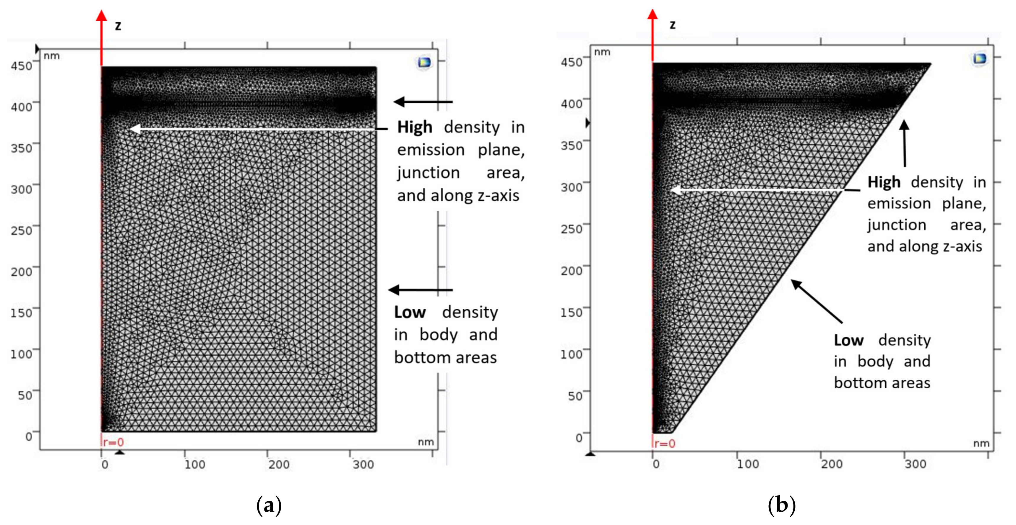
4.2. Mesh Density and Accuracy
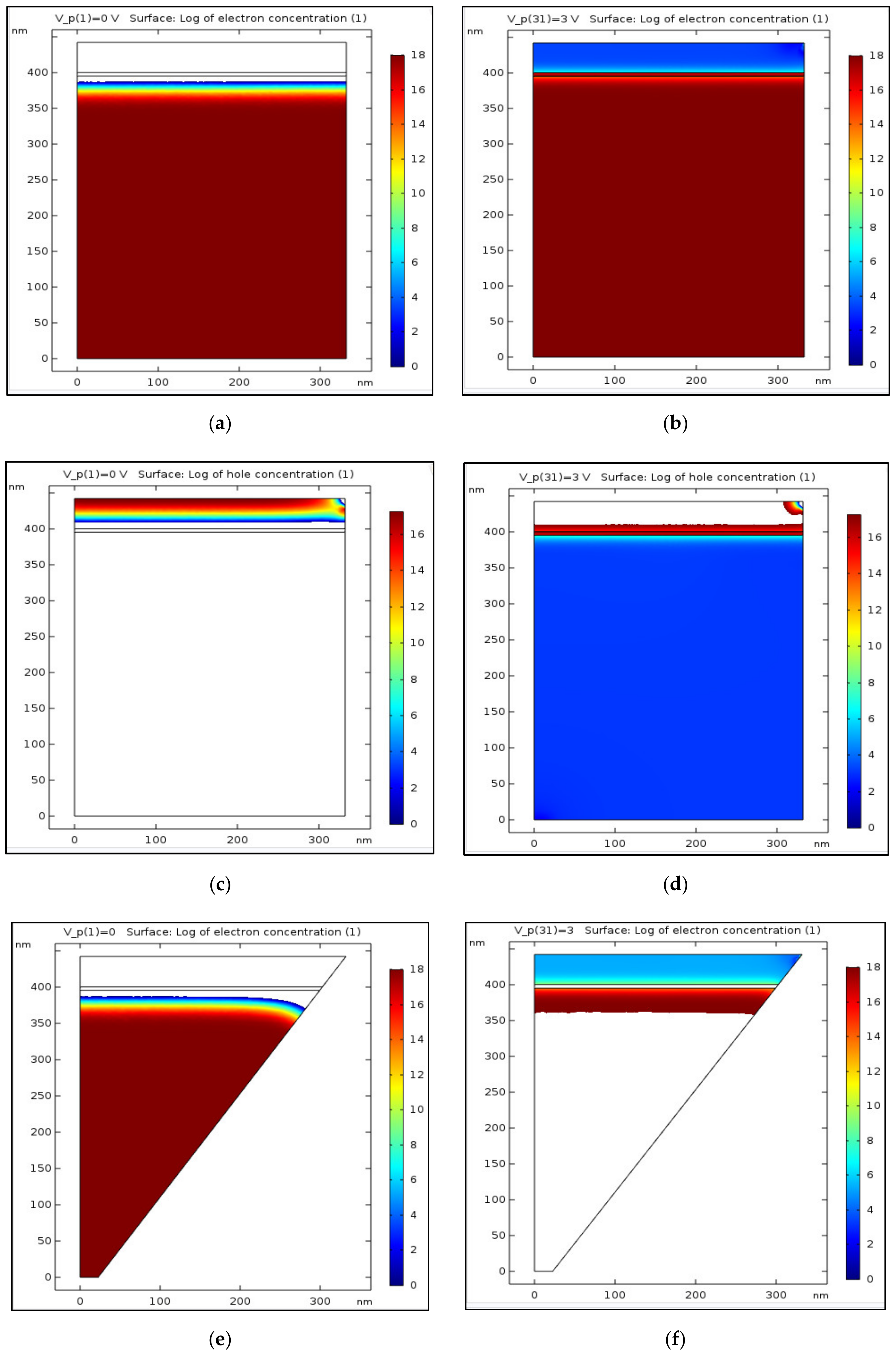
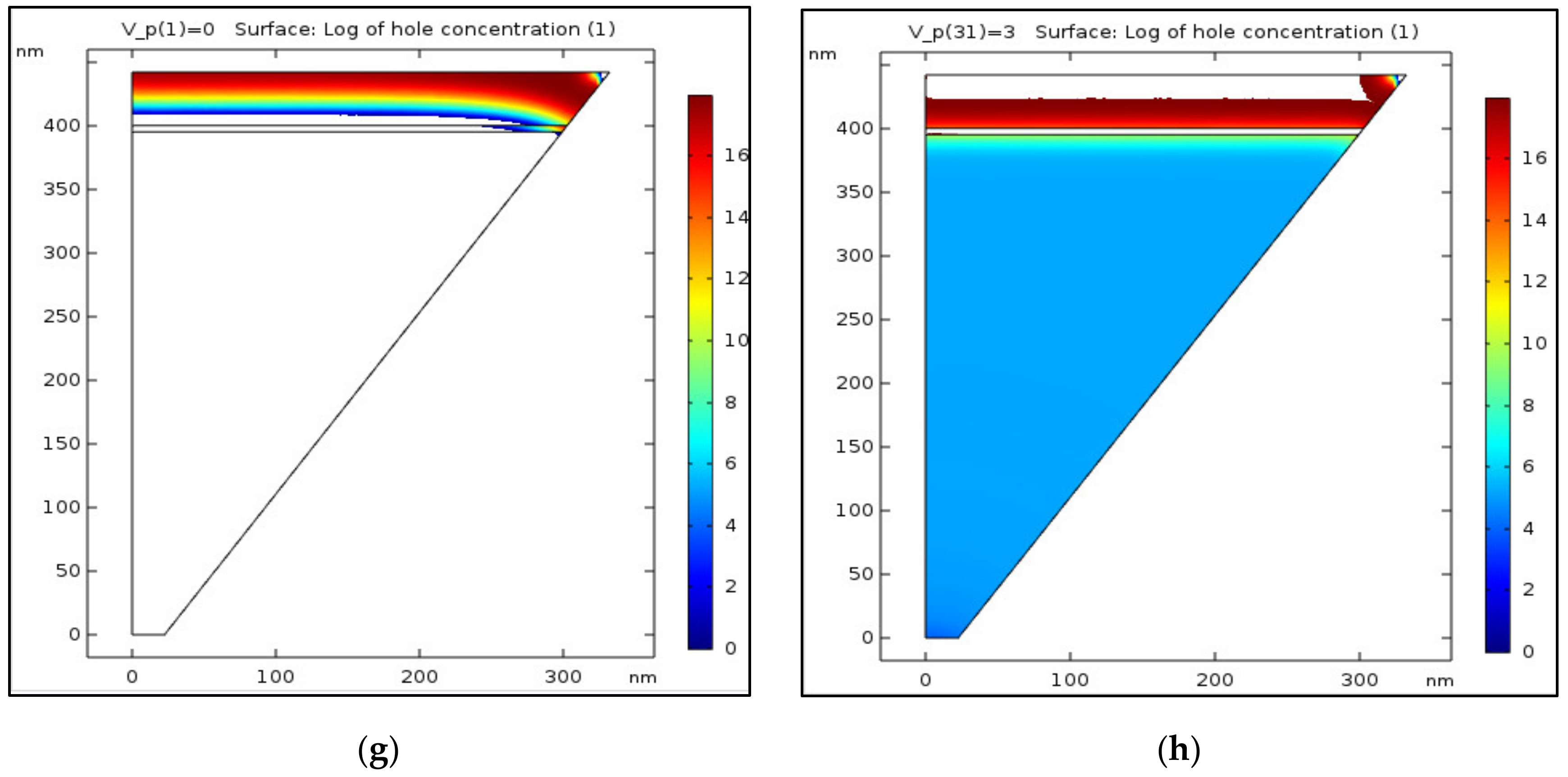
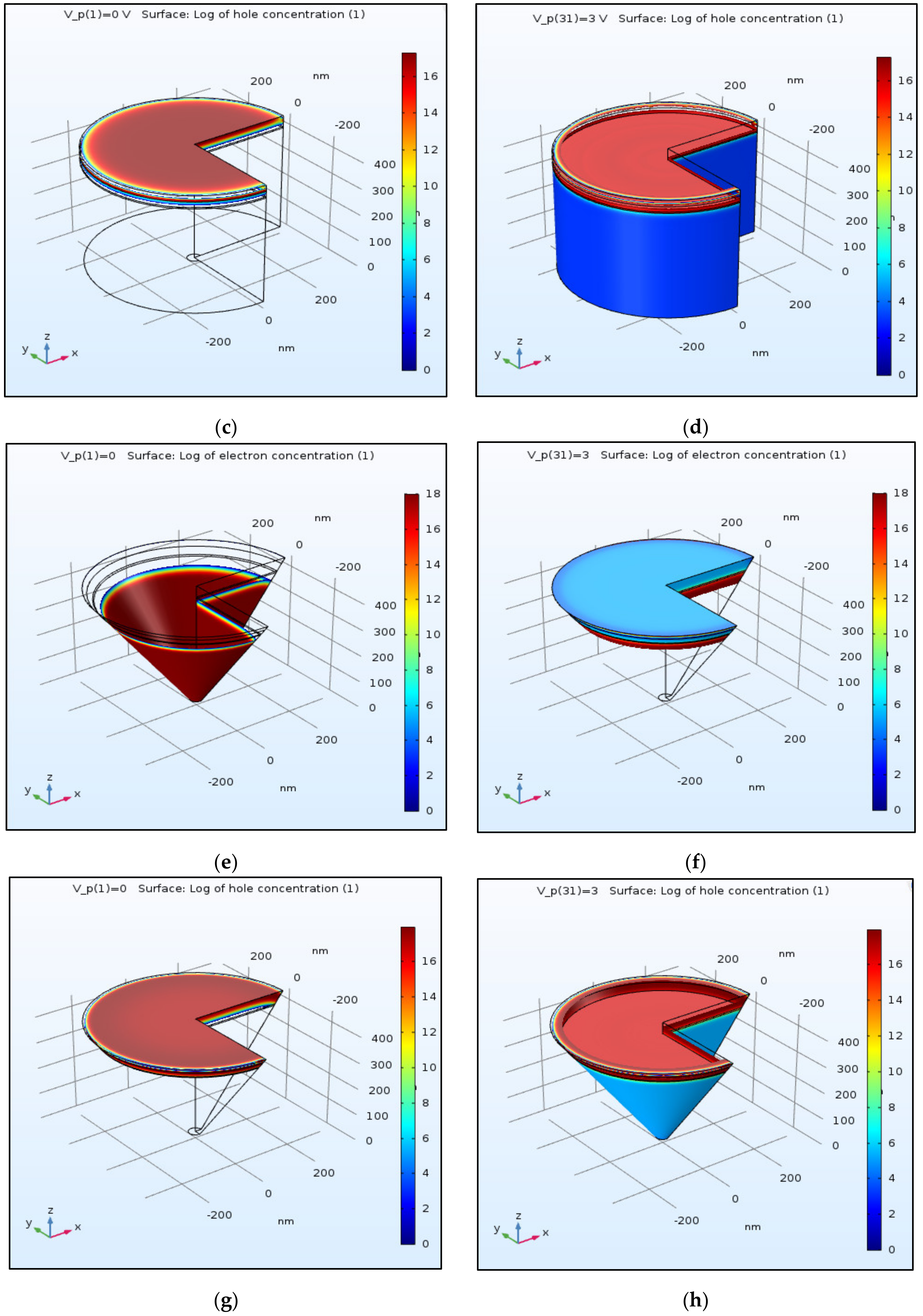
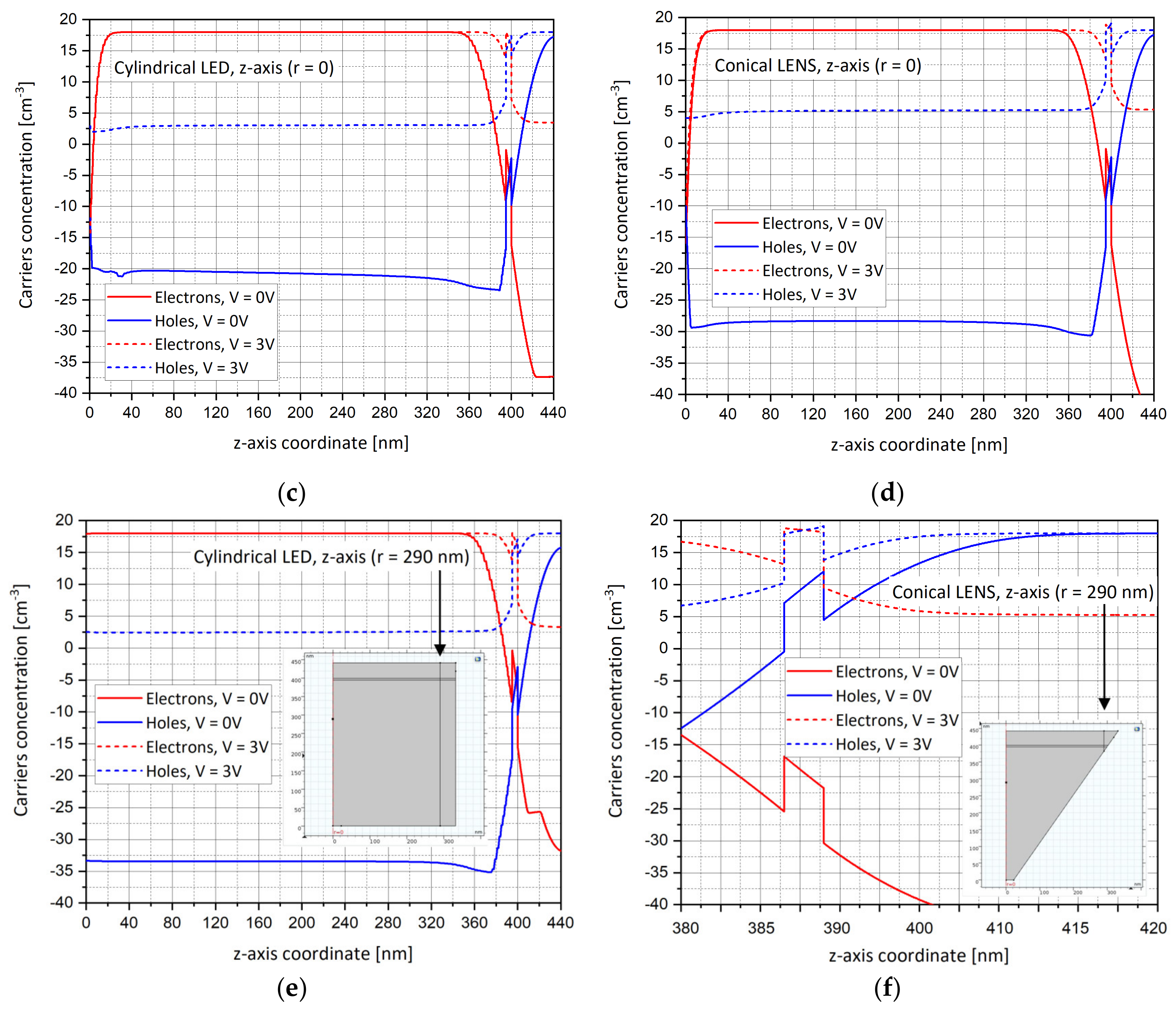
4.3. Electron and Hole Concentrations and Distribution (x-axis)
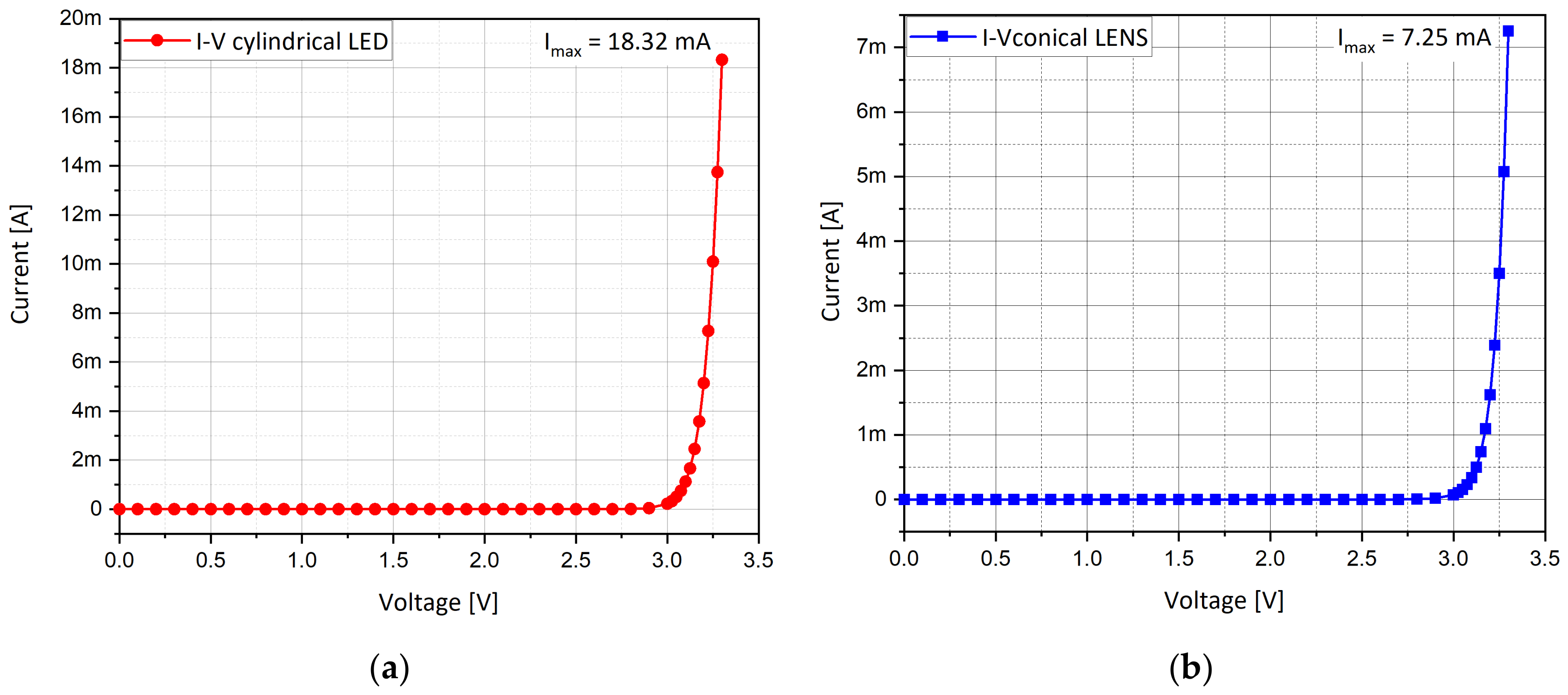
4.4. I-V Curves
- -
- r = is the radius of the cylinder’s circle,
- -
- h is the height of the cylinder.
- -
- r = is the radius of the cone’s small circle,
- -
- R = is the radius of the cone’s large circle,
- -
- h is the height of the cone.
4.5. Carriers Concentration Along x-axis and z-axis
5. Numerical Results—RGB Wavelength Optimization
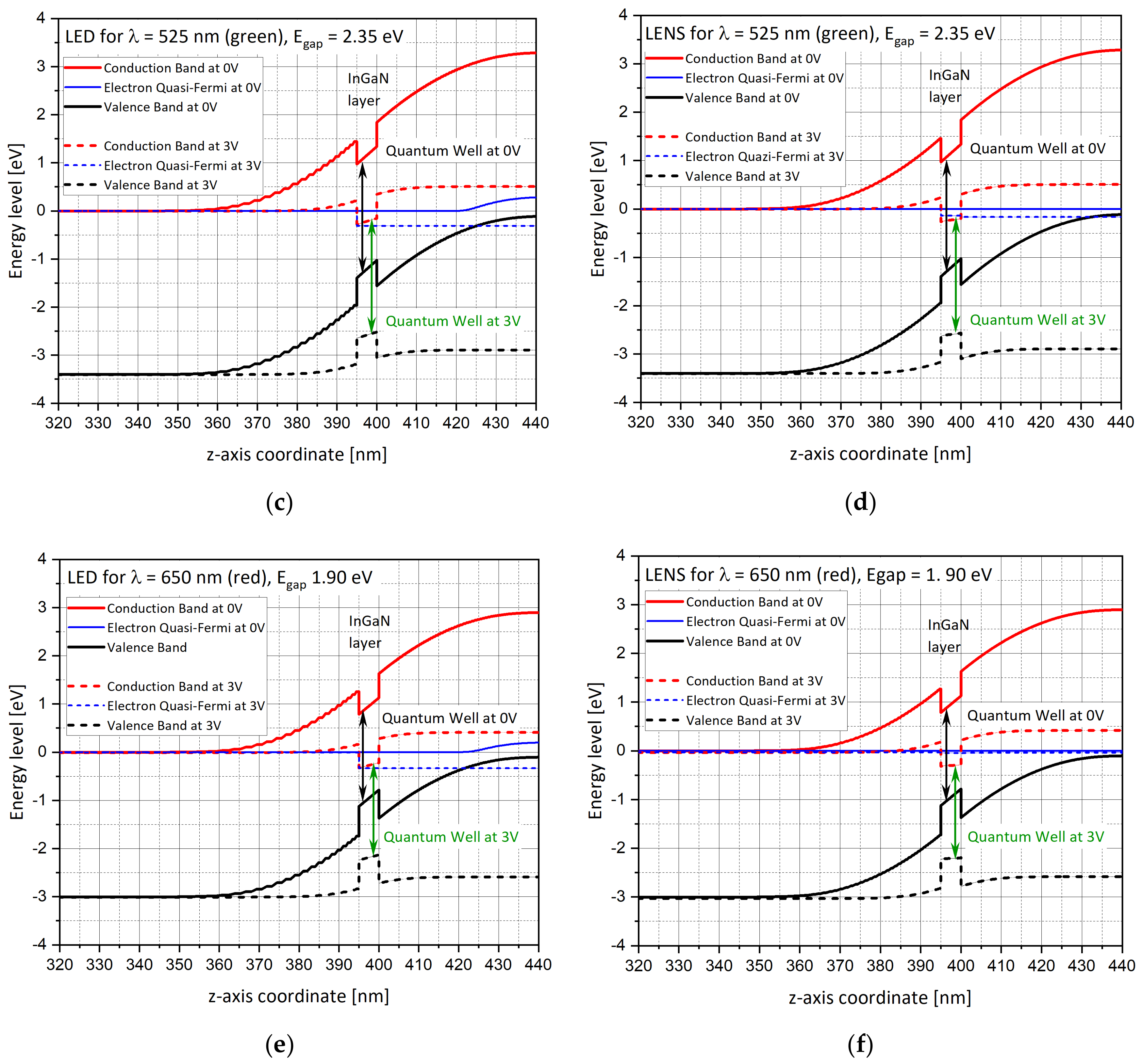
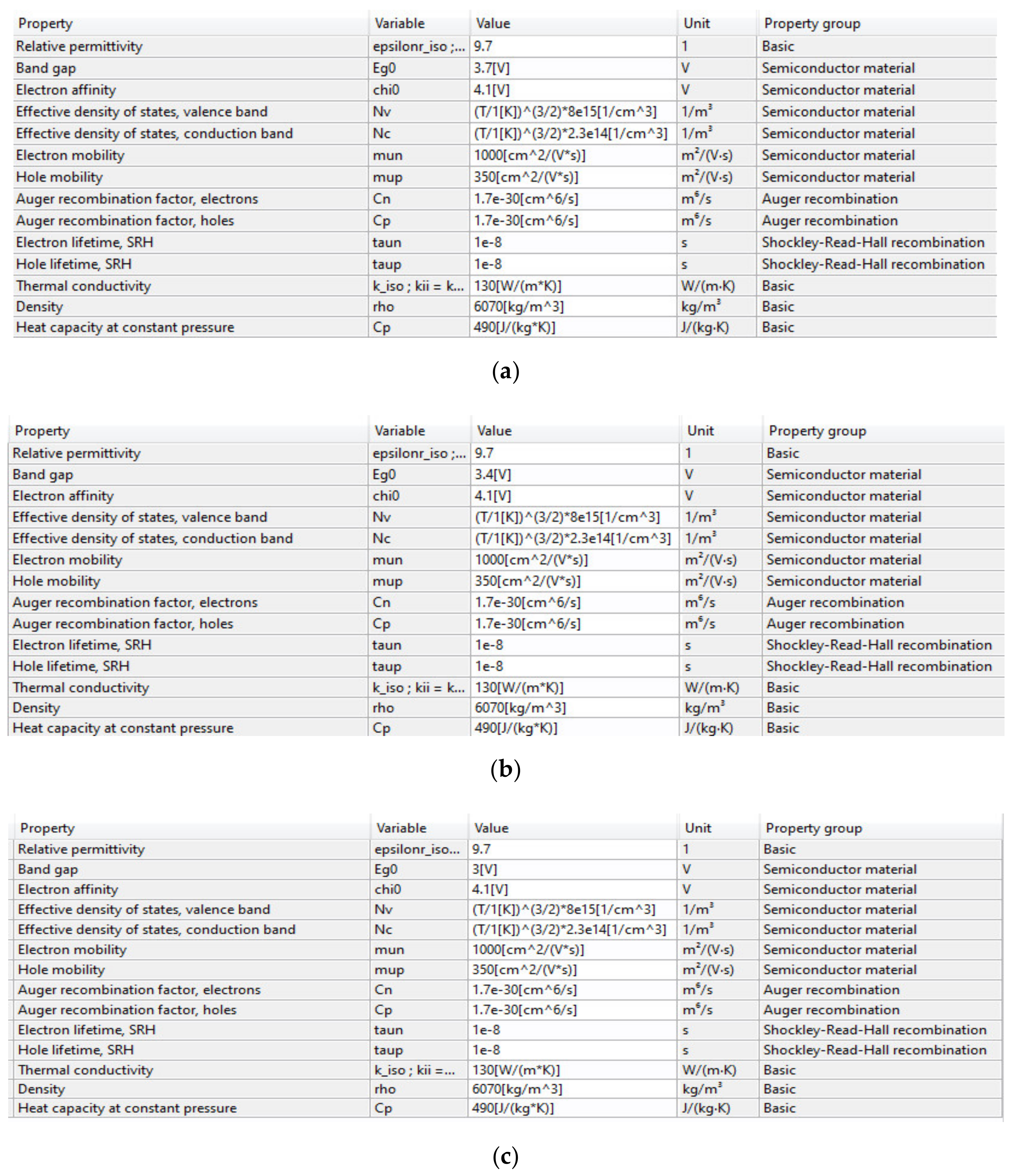
5.1. Energy Band Diagrams (z-axis, r = 0)
- -
- and are the effective densities of states in the conduction and valence bands;
- -
- is the band gap;
- -
- is Boltzmann’s constant;
- -
- is the lattice temperature.
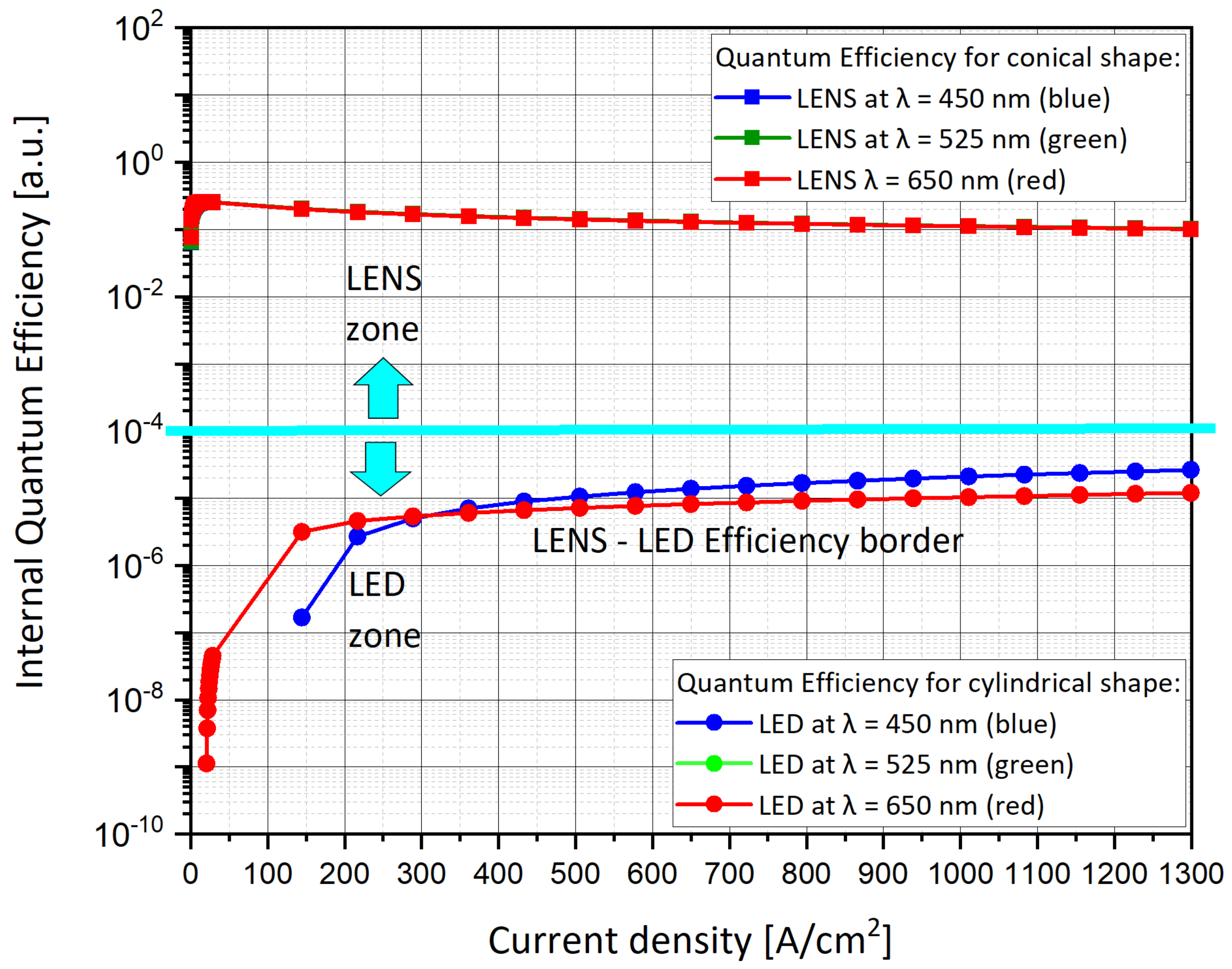
5.2. Efficiency Curve vs. Current Density
- -
- is the external quantum efficiency;
- -
- is the internal quantum efficiency;
- -
- is the transmission efficiency;
- -
- is the collection efficiency.
- -
- is the internal quantum efficiency;
- -
- is the rate of radiative recombination;
- -
- is the rate of non-radiative recombination.
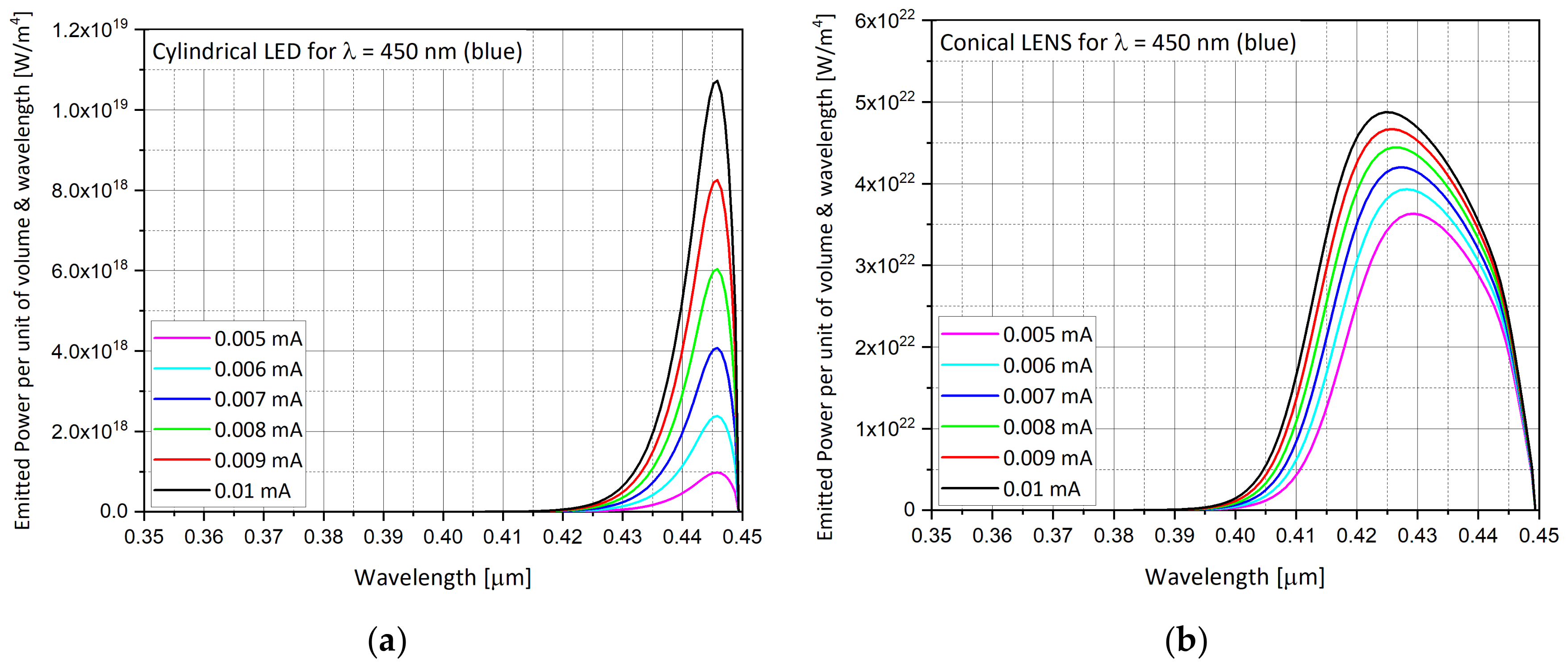
5.3. Emission Spectra from InGaN Layer
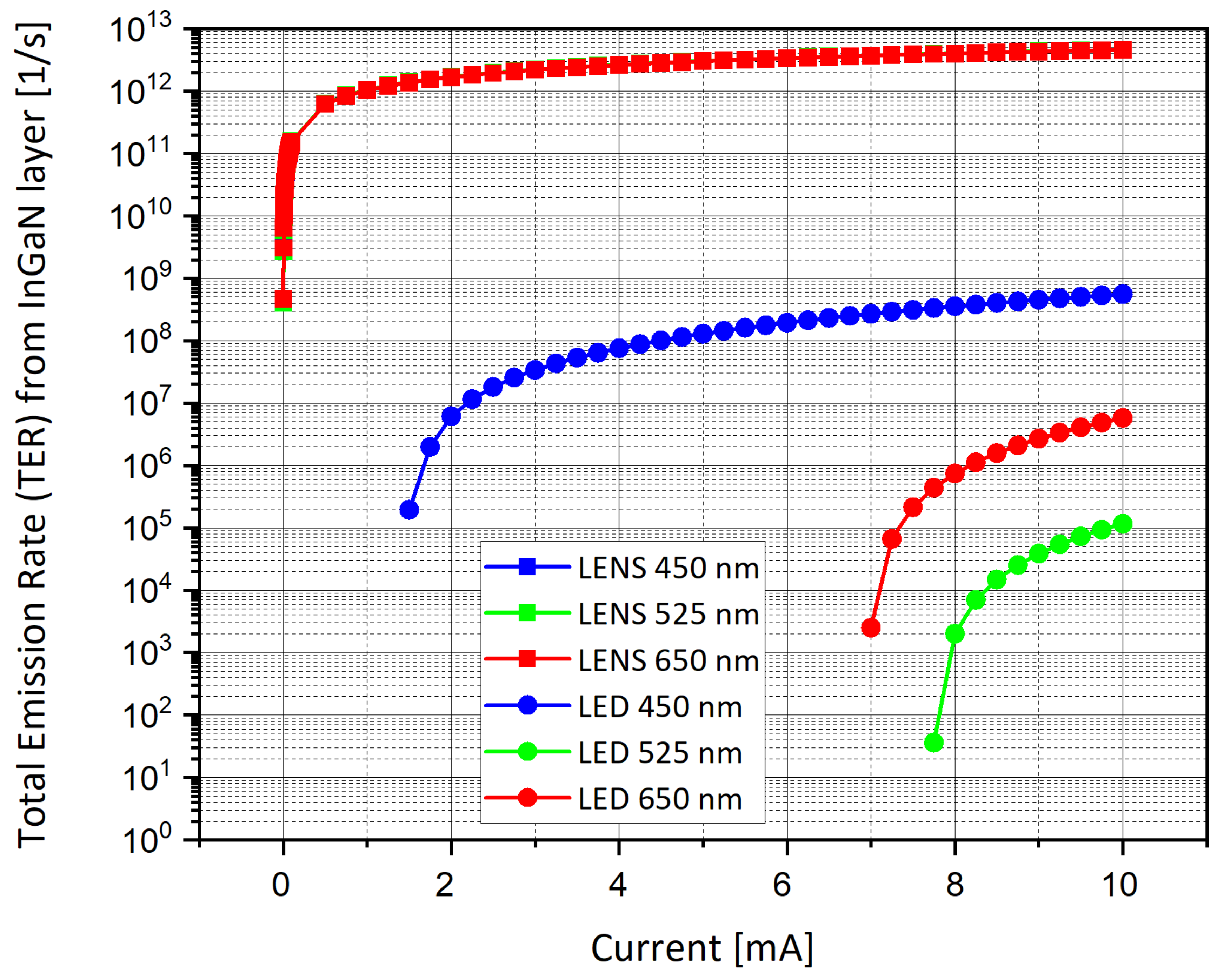
5.4. Total Emission Rate
- -
- is the light power output;
- -
- is the photon energy.
- -
- is the emission time;
- -
- is the quantity of emitted photon.
- -
- is the radiative recombination rate.
- -
- is the internal quantum efficiency;
- -
- is the non-radiative recombination rate.
6. Duality Applications
6.1. LENS as a Pixel for Nano-Display
6.2. LENS as a Light Emitting Device
7. Conclusions
8. Patents
Author Contributions
Funding
Conflicts of Interest
References
- Liu, Z.; Lin, C.-H.; Hyun, B.-R.; Sher, C.-W.; Lv, Z.; Luo, B.; Jiang, F.; Wu, T.; Ho, C.-H.; Kuo, H.-C.; et al. Micro-light-emitting diodes with quantum dots in display technology. Light Sci. Appl. 2020, 9, 1–23. [Google Scholar] [CrossRef] [PubMed]
- Hosseini, P.; Wright, C.D.; Bhaskaran, H. An optoelectronic framework enabled by low-dimensional phase-change films. Nature 2014, 511, 206–211. [Google Scholar] [CrossRef] [PubMed]
- Ra, Y.H.; Wang, R.; Woo, S.Y.; Djavid, M.; Sadaf, S.M.; Lee, J.; Botton, G.A.; Mi, Z. Full-Color Single Nanowire Pixels for Projection Displays. Nano Lett. 2016, 16, 4608–4615. [Google Scholar] [CrossRef] [PubMed]
- Basak, S.; Mohiddon, M.A.; Baumgarten, M.; Müllen, K.; Chandrasekar, R. Hierarchical multicolor nano-pixel matrices formed by coordinating luminescent metal ions to a conjugated poly(4′-octyl-2′,6′-bispyrazoyl pyridine) film via contact printing. Nat. Sci. Rep. 2015, 5, 8406. [Google Scholar] [CrossRef]
- Pimpin, A.; Srituravanich, W. Review on Micro- and Nanolithography Techniques and their Applications. Eng. J. 2012, 16, 37–55. [Google Scholar] [CrossRef]
- Carmigniani, J.; Furht, B. Handbook of Augmented Reality; Springer: New York, NY, USA, 2011; p. 129. [Google Scholar]
- Robinson, M.G.; Chen, J.; Sharp, G.D. Polarization Engineering for LCD Projection; J. Wiley & Sons Ltd.: Chichester, UK, 2005; p. 124. [Google Scholar]
- Zhang, Z.; You, Z.; Chu, D. Fundamentals of phase-only liquid crystal on silicon (LCOS) devices. Light Sci. Appl. 2014, 3, e213. [Google Scholar] [CrossRef]
- Tanaka, N. Sony’s OLED Micro-display Realizes Both Small Pixel Pitch, High Image Quality. 2017. Available online: http://techon.nikkeibp.co.jp/atclen/news_en/15mk/062001307/?ST=msbe (accessed on 1 September 2020).
- Hornbeck, L.J. Digital Light Processing and MEMS: An overview. In Proceedings of the Digest IEEE/Leos 1996 Summer Topical Meeting, Advanced Applications of Lasers in Materials and Processing, Keystone, CO, USA, 5–9 August 1996; Available online: https://ieeexplore.ieee.org/abstract/document/540770 (accessed on 1 September 2020).
- Armitage, D.; Underwood, I.; Wu, V. Emissive Microdisplays. In Introduction to Microdisplays; Wiley Series in Display Technology; John Wiley & Sons Ltd.: Chichester, UK, 2006; p. 237. [Google Scholar]
- Liu, J.-L.; Zhang, J.-L.; Wang, G.-X.; Mo, C.-L.; Xu, L.-Q.; Ding, J.; Quan, Z.J.; Wang, X.-L.; Pan, S.; Zheng, C.-D.; et al. Status of GaN-based green light-emitting diodes. Chin. Phys. B 2015, 24, 067804. [Google Scholar] [CrossRef]
- Eun, L.H.; Hong, K.J. How bright of luminance is needed for outdoor commercial display. In Proceedings of the 2016 IEEE 6th International Conference on Consumer Electronics, Berlin, Germany, 5–7 September 2016; pp. 141–144. [Google Scholar]
- Herrnsdorf, J.; McKendry, J.J.D.; Zhang, S.; Xie, E.; Ferreira, R.; Massoubre, D.; Zuhdi, A.M.; Henderson, R.K.; Underwood, I.; Watson, S.; et al. Active-Matrix GaN Micro Light-Emitting Diode Display with Unprecedented Brightness. IEEE Trans. Electron. Devices 2015, 62, 1918–1925. [Google Scholar] [CrossRef]
- Eisenfeld, T.; Karsenty, A. Super High Intensity Nano Emitting (SHINE) Pixel for High Resolution and High Brightness Displays. J. Nanophotonics 2019, 14, 016002. [Google Scholar] [CrossRef]
- Eisenfeld, T.; Karsenty, A. Design and Modeling of Light Emitting Nano-pixel Structure (LENS) for High Resolution Display (HRD) in Visible Range. Nanomaterials 2020, 10, 214. [Google Scholar] [CrossRef]
- Wang, S.W.; Hong, K.B.; Tsai, Y.L.; Teng, C.H.; Tzou, A.J.; Chu, Y.C.; Lee, P.T.; Ku, P.C.; Lin, C.C.; Kuo, H.C. Wavelength tunable InGaN/GaN nano-ring LEDs via nano-sphere lithography. Nat. Sci. Rep. 2017, 7, 42962. [Google Scholar] [CrossRef] [PubMed]
- Advanced Laboratory of Electro-Optics (ALEO). Available online: https://www.aleo.solutions/ (accessed on 1 September 2020).
- Holgate, S.A. Understanding Solid State Physics; CRC Press: Boca Raton, FL, USA, 2009; pp. 177–178. [Google Scholar]
- Li, Q.; Westlake, K.R.; Crawford, M.H.; Lee, S.R.; Koleske, D.D.; Figiel, J.J.; Cross, K.C.; Fathololoumi, S.; Mi, Z.; Wang, G.T. Optical performance of top-down fabricated InGaN/GaN nanorod light emitting diode arrays. Opt. Express 2011, 19, 25528–25534. [Google Scholar] [CrossRef] [PubMed]
- Zhang, H.; Jacopin, G.; Neplokh, V.; Largeau, L.; Julien, F.H.; Kryliouk, O.; Tchernycheva, M. Color control of nanowire InGaN/GaN light emitting diodes by post-growth treatment. Nanotechnology 2015, 26, 465203. [Google Scholar] [CrossRef] [PubMed]
- Li, C.C.; Zhan, J.L.; Chen, Z.Z.; Jiao, F.; Chen, Y.F.; Chen, Y.Y.; Nie, J.X.; Kang, X.N.; Li, S.F.; Wang, Q.; et al. Operating behavior of micro-LEDs on a GaN substrate at ultrahigh injection current densities. Opt. Express 2019, 16, A1146–A1155. [Google Scholar] [CrossRef] [PubMed]
- Chen, J. Electrical Simulation and Current Spreading Analysis in the GaN-based Light-Emitting Diode Devices. Comsol Tech. Pap. Present. Comsol Website. 2011. Available online: https://www.comsol.com/paper/electrical-simulation-and-current-spreading-analysis-in-the-gan-based-light-emit-12479 (accessed on 1 September 2020).
- Pooley, M. Investigating LED Efficiency via Multiphysics Simulation. Comsol Tech. Pap. Present. 2014. Comsol Website. Available online: https://www.comsol.com/blogs/investigating-led-efficiency-via-multiphysics-simulation/ (accessed on 1 September 2020).
- Happich, J. Researchers Grow Efficient InGaN LEDs for Green and Red. EeNewsAnalog 2019. Available online: https://www.eenewsanalog.com/news/researchers-grow-efficient-ingan-leds-green-and-red (accessed on 1 September 2020).
- Armitage, D.; Underwood, I.; Wu, S.T. Transmissive Liquid Crystal Microdisplays. In Introduction to Microdisplays; Wiley Series in Display Technology; John Wiley & Sons Ltd.: Chichester, UK, 2006; p. 151. [Google Scholar]
- Held, G. Introduction to Light Emitting Diode Technology and Applications, 1st ed.; CRC Press: Boca Raton, FL, USA, 2008; p. 4. [Google Scholar]
- Rockwell Collins, F-35 Gen III Helmet Mounted Display System. Available online: https://www.rockwellcollins.com/ (accessed on 1 September 2020).
- Mahan, J.R. The Monte Carlo Ray-Trace Method in Radiation Heat Transfer and Applied Optics; Wiley: New York, NY, USA, 2018. [Google Scholar]
- David, A.; Benisty, H.; Weisbuch, C. Optimization of Light-Diffracting Photonic-Crystals for High Extraction Efficiency LEDs. J. Disp. Technol. 2007, 3, 133–148. [Google Scholar] [CrossRef]
- Khoshnegar, M.; Eftekharian, A.; Sodagar, M.; Khorasani, S.; Adibi, A. Quantum well design and diffraction efficiency of quantum well light emitting diode. SPIE 2009, 7223, 722311. [Google Scholar]
- Kikuta, H.; Hino, S.; Maruyama, A. Estimation method for the light extraction efficiency of light-emitting elements with a rigorous grating diffraction theory. J. Opt. Soc. Am. A 2006, 23, 1207–1213. [Google Scholar] [CrossRef]
- Benisty, H.; Danglot, J.; Talneau, A.; Enoch, S.; Pottage, J.M.; David, A. Investigation of Extracting Photonic Crystal Lattices for Guided Modes of GaAs-Based Heterostructures. IEEE J. Quantum Electron. 2008, 44, 777–789. [Google Scholar] [CrossRef]
- Winston, R.; Miñano, J.C.; Benítez, P. Nonimaging Optics, 1st ed.; Elsevier Academic Press: Amsterdam, The Netherlands, 2004. [Google Scholar]
- Cassarly, W. Nonimaging optics: Concentration and illumination. In OSA Handbook of Optics; McGraw-Hill: New York, NY, USA, 2001; Volume III. [Google Scholar]
- LightTools Illumination Design Software, Synopsys. Available online: https://www.synopsys.com/optical-solutions/lighttools.html (accessed on 1 September 2020).
- Comsol Multi-Physics Software Package Website. Available online: https://www.comsol.com/ (accessed on 1 September 2020).
- Karsenty, A.; Mandelbaum, Y. Computer Algebra Challenges in Nanotechnology: Accurate Modeling of nanoscale electro-optic devices using Finite Elements Method. Math. Comput. Sci. 2019, 13, 117–130. [Google Scholar] [CrossRef]
- Light Propagation Modelling Using COMSOL Multiphysics; Medical Optics Course Atomic Physics Lund University; Biophotonics Group, Lund University: Lund, Sweden; Available online: http://www.atomic.physics.lu.se/fileadmin/atomfysik/Biophotonics/Education/MultiphysicsExercise.pdf (accessed on 1 September 2020).
- Rashid, S.; Wahid, M.H.A.; Ahmad Hambali, N.A.M.; Abdul Halim, N.S.A.; Ramli, M.M.; Shahimin, M.M. Emission rate and internal quantum efficiency enhancement in different geometrical shapes of GaN LED. AIP Conf. Proc. 2017, 1885, 020284. [Google Scholar] [CrossRef]
- Li, G.; Song, W.; Wang, H.; Luo, X.; Luo, X.; Li, S. Performance Improvement of UV Light-Emitting Diodes with Triangular Quantum Barriers. IEEE Photonics Technol. Lett. 2018, 30, 1071–1074. [Google Scholar] [CrossRef]
- Palmer, D.W. Energy-Gap Values for Hexagonal InxGa1-xN and InN. 2004. Available online: http://www.semiconductors.co.uk/eg(ingan).htm (accessed on 1 September 2020).
- Mesrane, A.; Rahmoune, F.; Mahrane, A.; Oulebsir, A. Design and Simulation of InGaN 𝑝-𝑛 Junction Solar Cell. Int. J. Photoenergy 2015, 2015, 9. [Google Scholar] [CrossRef]
- Pratiyush, A.S.; Krishnamoorthy, S.; Muralidharan, R.; RajaN, S.; Nath, D.N. Advances in Ga2O3 solar-blind UV photodetectors. Gallium Oxide Technol. Devices Appl. Met. Oxides 2019, 16, 369–399. [Google Scholar] [CrossRef]
- Hui, R. Light sources for optical communications. Introd. Fiber-Opt. Commun. 2020, 3, 77–124. [Google Scholar]
- Belhassen, J.; Frisch, A.; Kapellner, Y.; Zalevsky, Z.; Karsenty, A. V-groove-shaped silicon-on-insulator photopolarized activated modulator (SOIP2AM): A polarizing transistor. J. Opt. Soc. Am. A 2020, 37, 46–55. [Google Scholar] [CrossRef] [PubMed]
- Bennett, A.; Gadassi, I.; Priel, Z.; Mandelbaum, Y.; Karsenty, A.; Luc, T.; Chelly, A.; Shlimak, I.; Zalevsky, Z. Fast Optoelectronic Responsivity of metal-oxide-semiconductor nanostructures. J. Nanophotonics 2016, 10, 036001. [Google Scholar] [CrossRef]
- Rudnitsky, A.; Agdarov, S.; Gulitsky, K.; Zalevsky, Z. Silicon based mechanic-photonic wavelength converter for infrared photo-detection. Opt. Commun. 2017, 392, 114–118. [Google Scholar] [CrossRef]







| Parameters | Parameters Definition | Cylindrical LED | Conical LENS |
|---|---|---|---|
| Device dimensions and parameters: | |||
| RUem | InGaN Emitting layer Upper Radius | 332 nm | 302.59 nm |
| RLem | InGaN Emitting layer Lower Radius | 332 nm | 299.09 nm |
| AUem | InGaN Emitting layer Upper Area | 0.346 μm2 | 0.287 μm2 |
| ALem | InGaN Emitting layer Lower Area | 0.346 μm2 | 0.281 μm2 |
| Dbase | n-GaN Base diameter | 664 nm | 45 nm |
| Dtop | p-GaN Top surface diameter | 664 nm | 664 nm |
| OH | Overall Height | 442 nm | 442 nm |
| tem | InGaN Emitting layer distance from top LED surface | 42 nm | 42 nm |
| tInGaN | InGaN Emitting layer thickness | 5 nm | 5 nm |
| tsub | InGaN Emitting layer distance from bottom LED surface | 395 nm | 395 nm |
| Comsol setup used parameters: | |||
| Vp | P-GaN applied Voltage | 0 V–3 V | 0 V–3 V |
| Ip | Applied Current | 1 × 10⁻⁶–1 × 10⁻³ A | 1 × 10⁻⁶–1 ×10⁻³ A |
| p-GaN_up | Doping concentration of p-GaN upper layer | 1 × 1018 cm−3 | 1 × 1018 cm−3 |
| n-GaN_lo | Doping concentration of n-GaN lower layer | 1 × 1018 cm−3 | 1 × 1018 cm−3 |
| InGaN | Doping concentration of InGaN embedded layer | intrinsic | intrinsic |
| EBG InGaN | InGaN Energy Bandgap for λ = 450 nm (blue) | 2.759 V | 2.759 V |
| VBG GaN 450 | GaN Energy Bandgap for λ = 450 nm (blue) | 3.7 V | 3.7 V |
| VBG GaN 525 | GaN Energy Bandgap for λ = 525 nm (green) | 3.4 V | 3.4 V |
| VBG GaN 650 | GaN Energy Bandgap for λ = 650 nm (red) | 3.0 V | 3.0 V |
Publisher’s Note: MDPI stays neutral with regard to jurisdictional claims in published maps and institutional affiliations. |
© 2020 by the authors. Licensee MDPI, Basel, Switzerland. This article is an open access article distributed under the terms and conditions of the Creative Commons Attribution (CC BY) license (http://creativecommons.org/licenses/by/4.0/).
Share and Cite
Perlman, H.; Eisenfeld, T.; Karsenty, A. Performance Enhancement and Applications Review of Nano Light Emitting Device (LED). Nanomaterials 2021, 11, 23. https://doi.org/10.3390/nano11010023
Perlman H, Eisenfeld T, Karsenty A. Performance Enhancement and Applications Review of Nano Light Emitting Device (LED). Nanomaterials. 2021; 11(1):23. https://doi.org/10.3390/nano11010023
Chicago/Turabian StylePerlman, Harel, Tsion Eisenfeld, and Avi Karsenty. 2021. "Performance Enhancement and Applications Review of Nano Light Emitting Device (LED)" Nanomaterials 11, no. 1: 23. https://doi.org/10.3390/nano11010023
APA StylePerlman, H., Eisenfeld, T., & Karsenty, A. (2021). Performance Enhancement and Applications Review of Nano Light Emitting Device (LED). Nanomaterials, 11(1), 23. https://doi.org/10.3390/nano11010023


