Surface Nanostructuring during Selective Area Epitaxy of Heterostructures with InGaAs QWs in the Ultra-Wide Windows

 , , ,
, , ,
Abstract
:1. Introduction
2. Materials and Methods
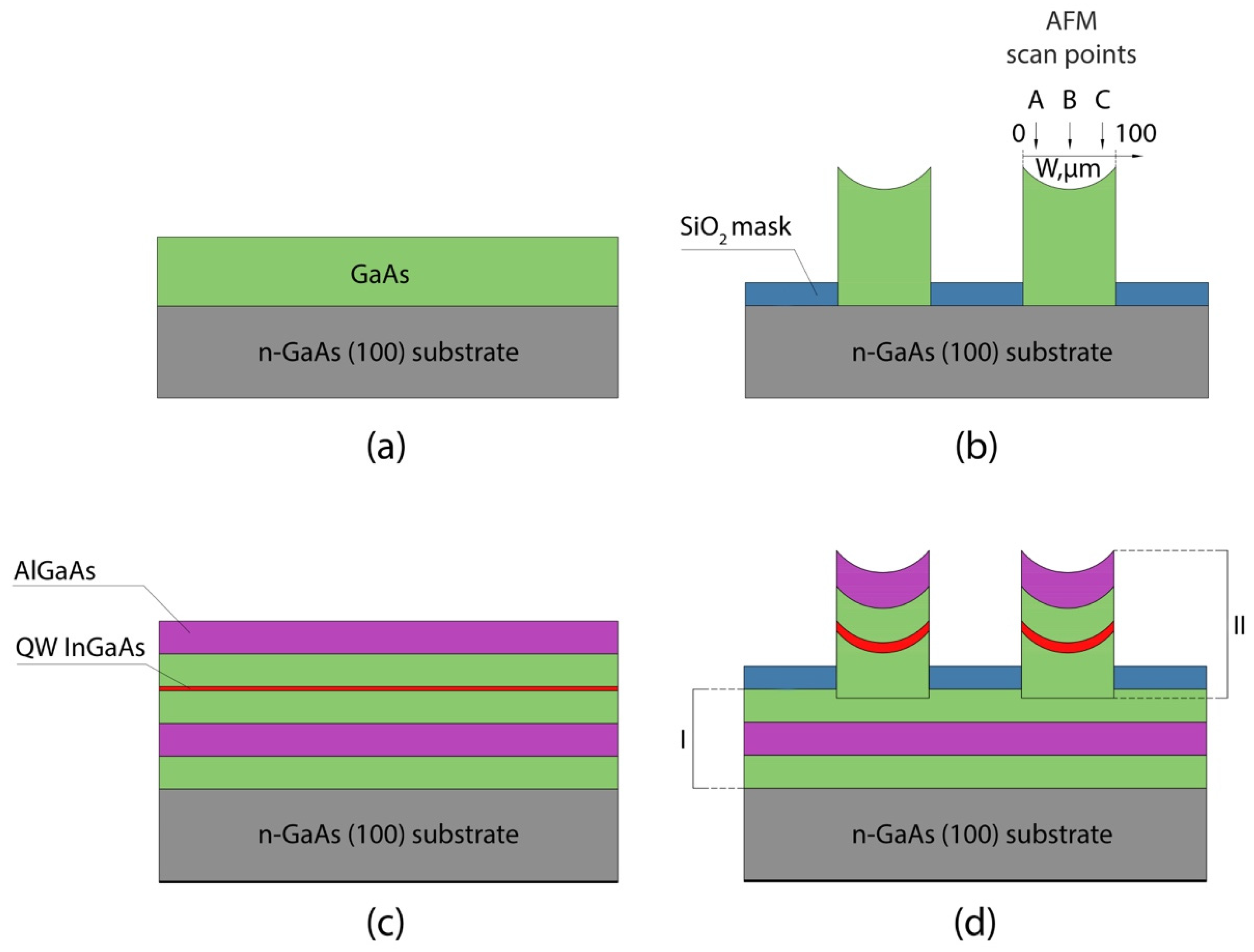
2.1. Samples
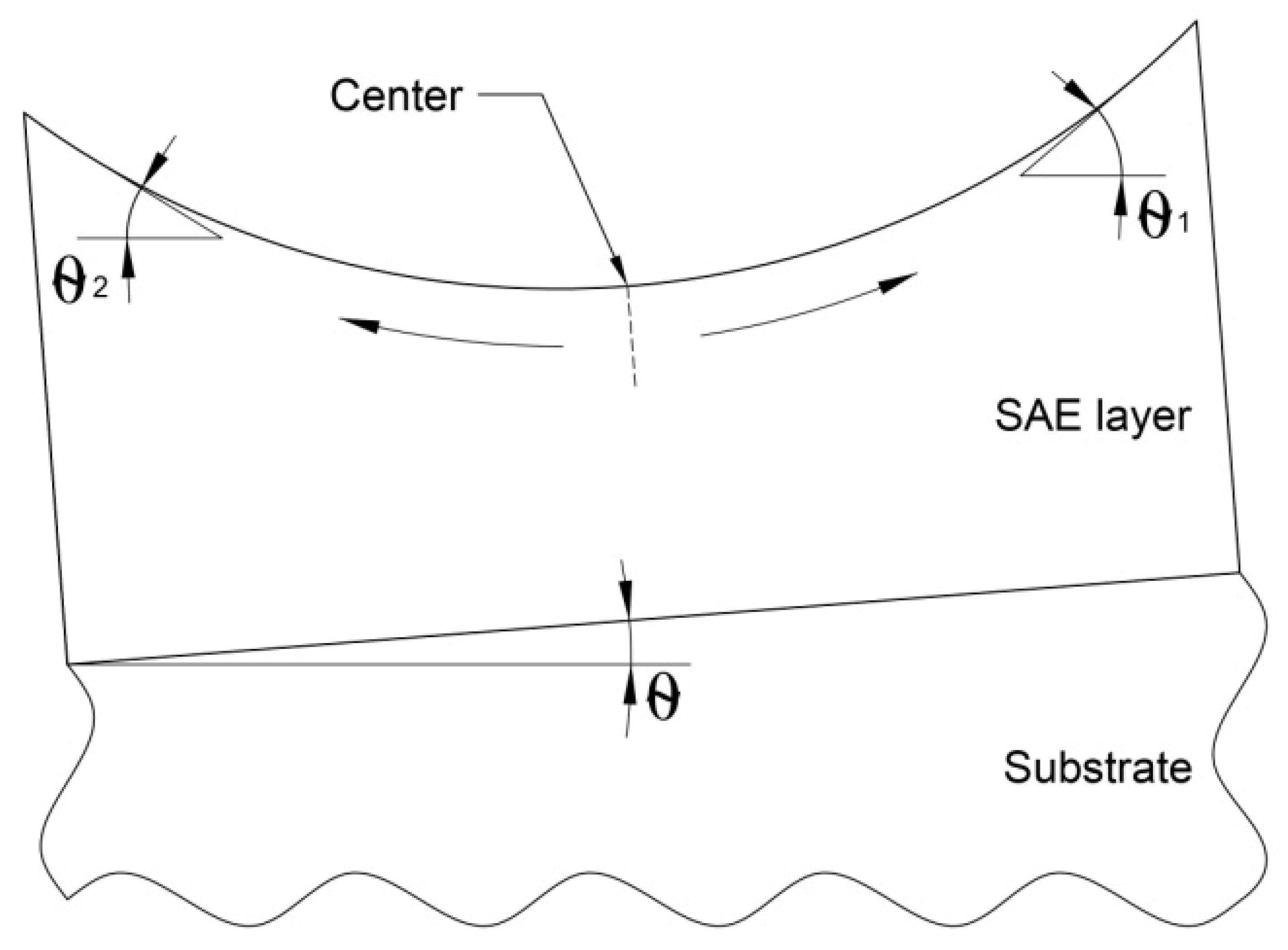
2.2. SAE Simulation Model
3. Results and Discussion
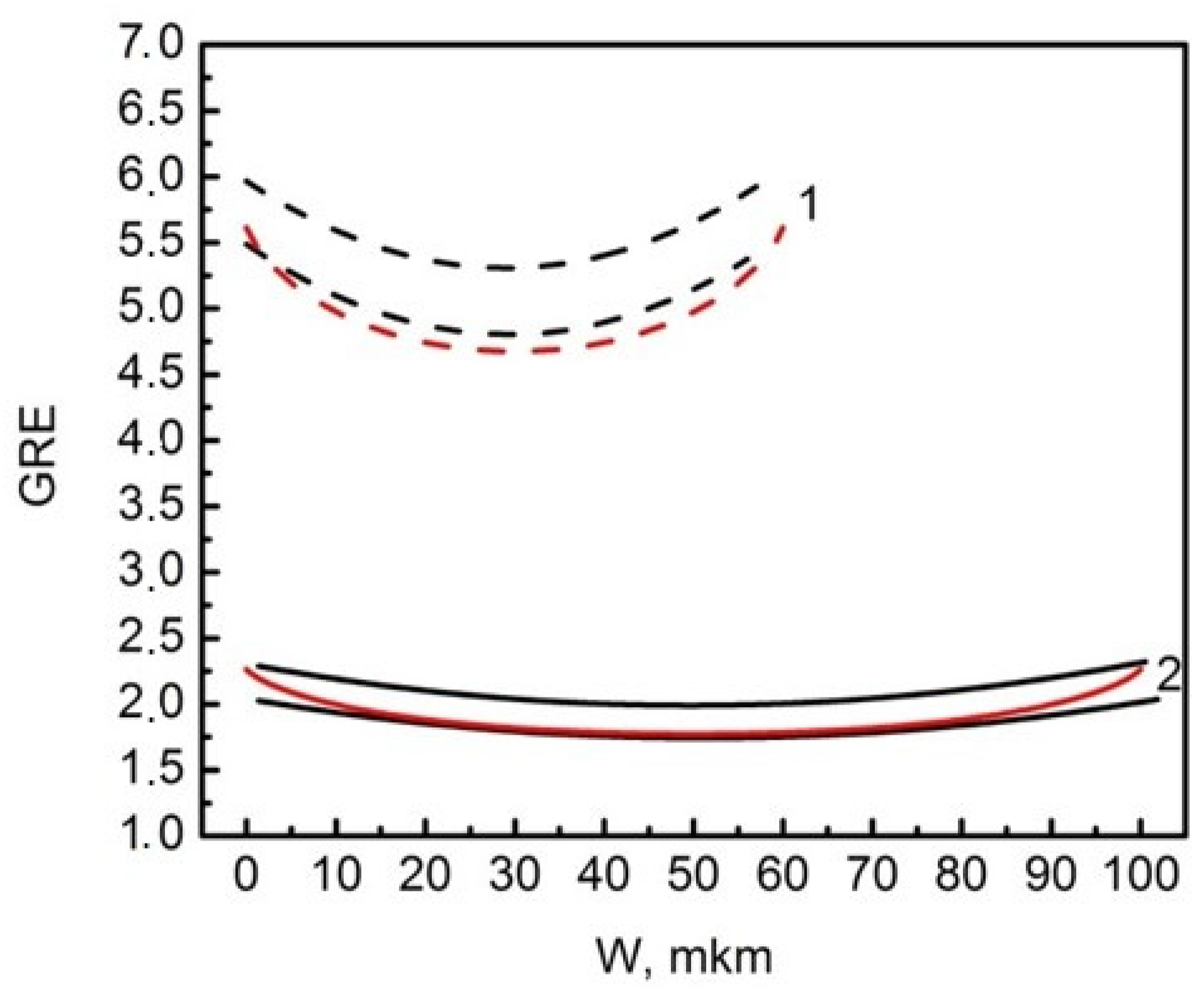
3.1. Growth Rate Enhancement (GRE) Effect in GaAs Layers Grown by SAE
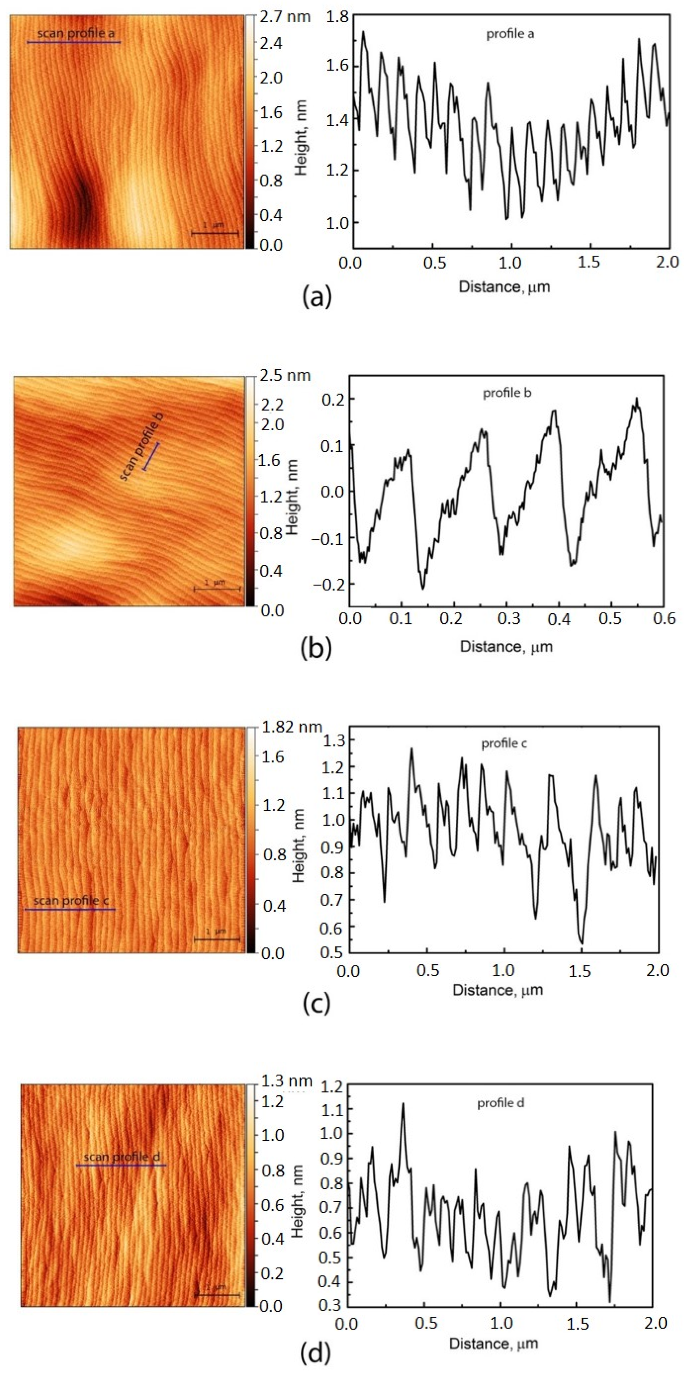
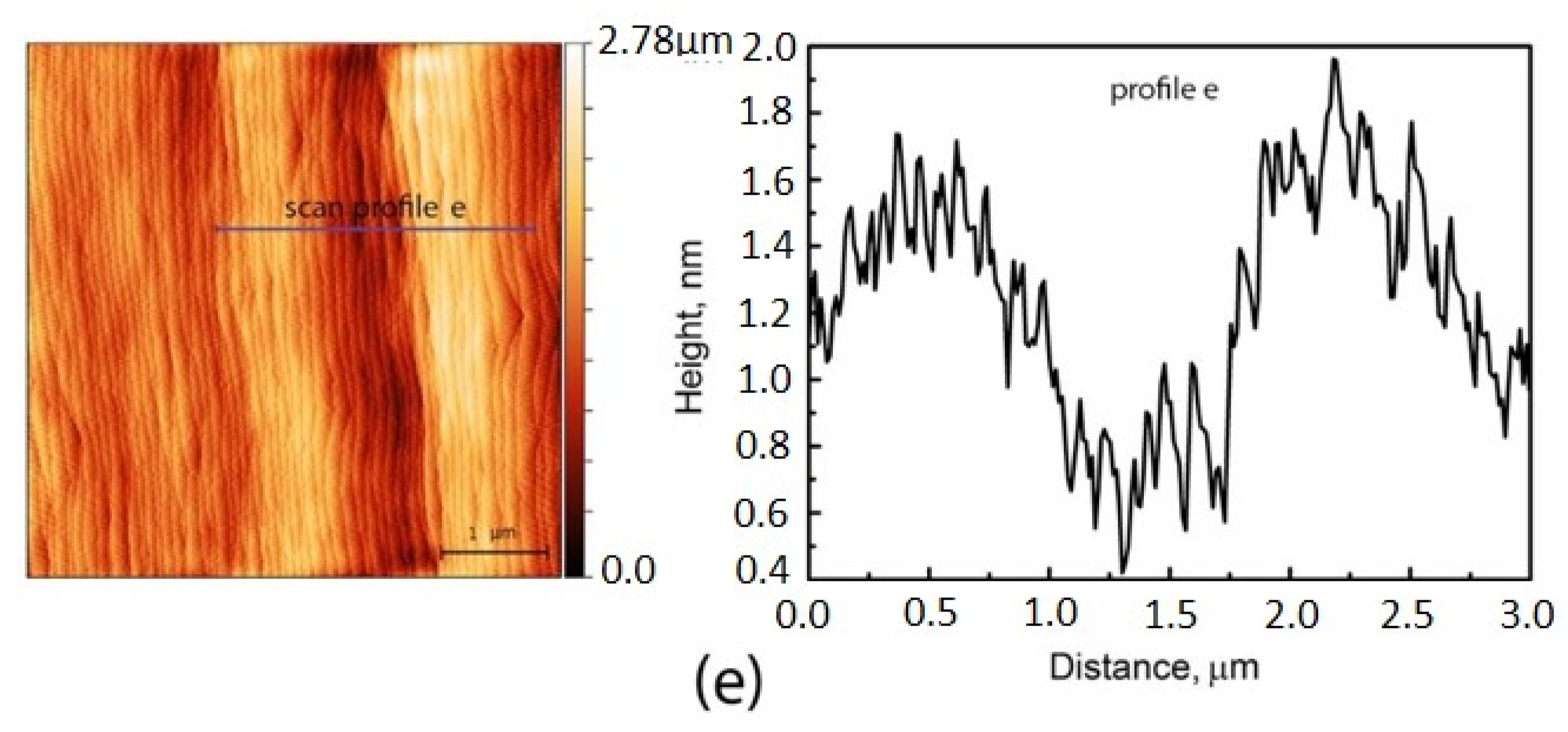
3.2. Surface Morphology of GaAs Layers
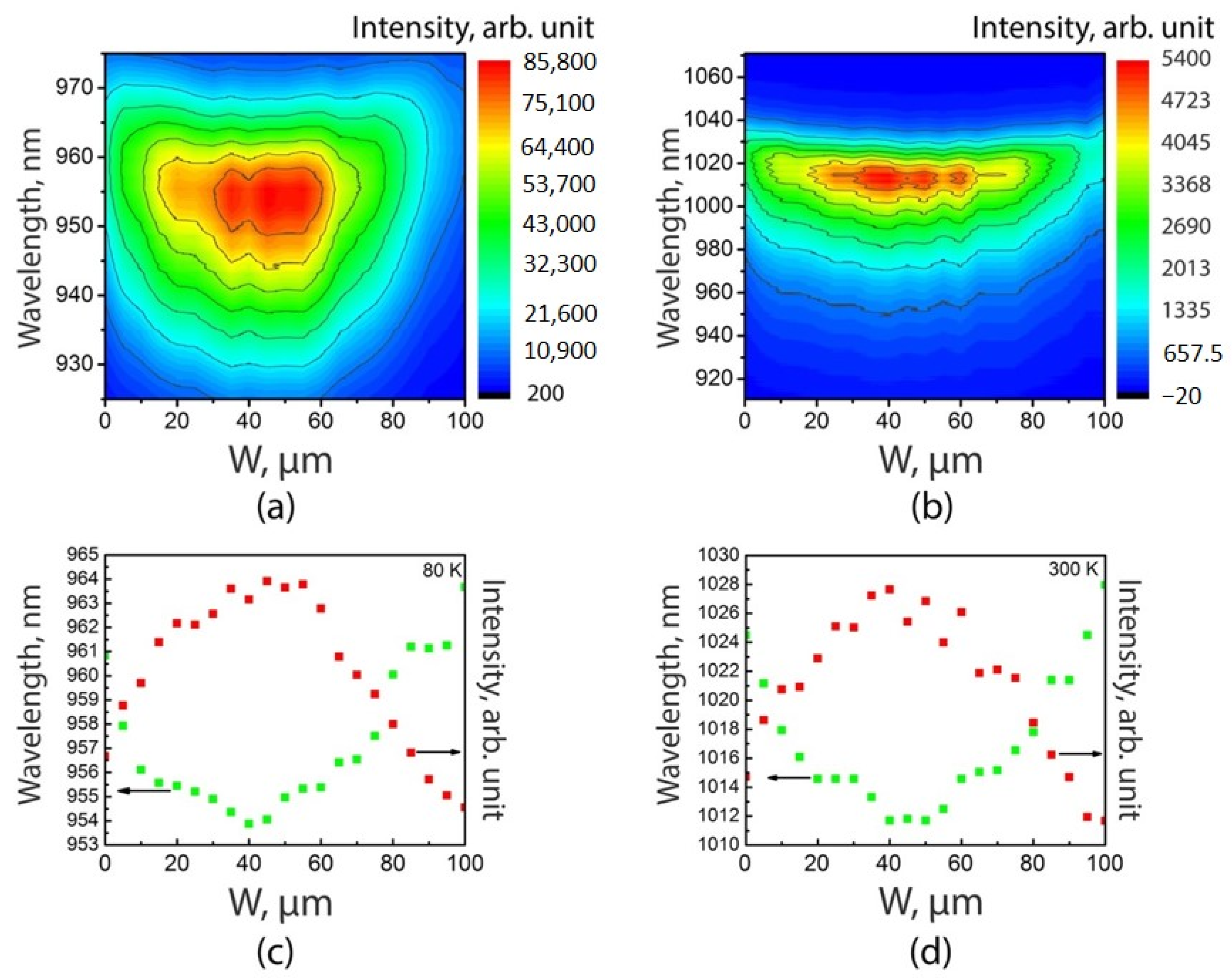
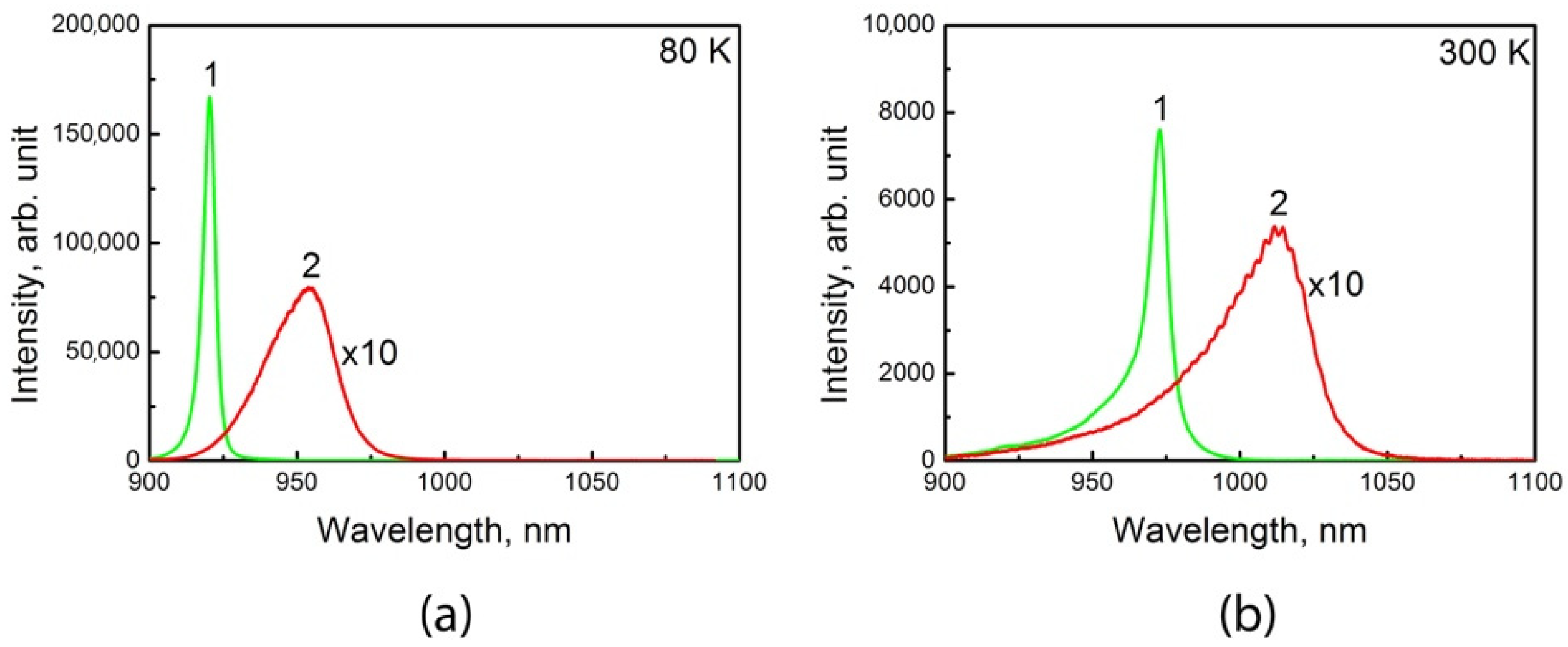
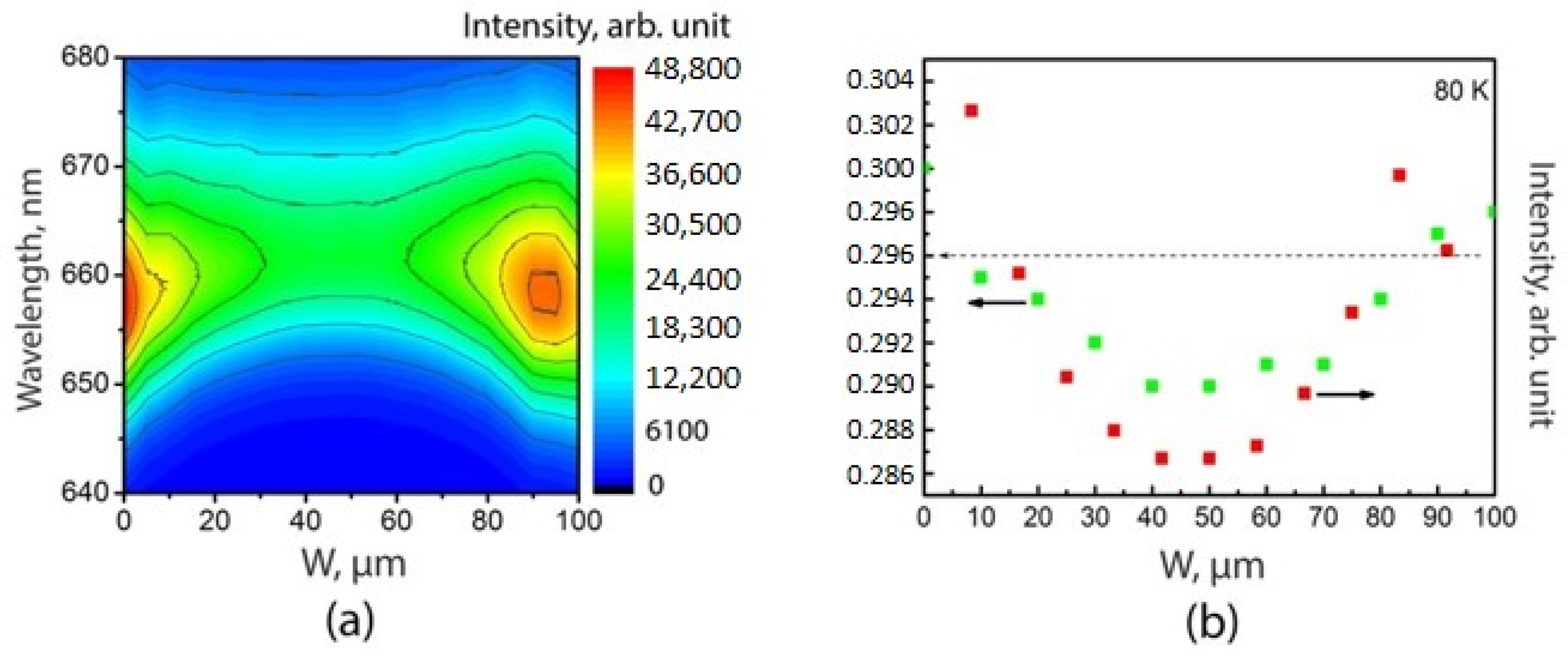
3.3. Microphotoluminescence Spectra
4. Conclusions
Author Contributions
Funding
Data Availability Statement
Conflicts of Interest
References
- Williams, K.A.; Bente, E.A.J.M.; Heiss, D.; Jiao, Y.; Ławniczuk, K.; Leijtens, X.J.M.; van der Tol, J.J.G.M.; Smit, M.K. InP photonic circuits using generic integration [Invited]. Photon. Res. 2015, 3, B60–B68. [Google Scholar] [CrossRef]
- Zhang, C.; Li, X. III–V nanowire transistors for low-power logic applications: A review and outlook. IEEE Trans. Electron. Devices 2016, 63, 223–234. [Google Scholar] [CrossRef]
- Dietrich, C.P.; Fiore, A.; Thompson, M.G.; Kamp, M.; Höfling, S. GaAs integrated quantum photonics: Towards compact and multi: Functional quantum photonic integrated circuits. Laser Photonics Rev. 2016, 10, 870–894. [Google Scholar] [CrossRef] [Green Version]
- Zhang, C.; Miao, X.; Chabak, K.D.; Li, X. A review of III–V planar nanowire arrays: Selective lateral VLS epitaxy and 3D transistors. J. Phys. D Appl. Phys. 2017, 50, 393001. [Google Scholar] [CrossRef]
- Bogdanov, S.; Shalaginov, M.Y.; Boltasseva, A.; Shalaev, V.M. Material platforms for integrated quantum photonics. Opt. Mater. Express 2017, 7, 111–132. [Google Scholar] [CrossRef]
- Smit, M.; Williams, K.; van der Tol, J. Past, present, and future of InP-based photonic integration. APL Photonics 2019, 4, 050901. [Google Scholar] [CrossRef] [Green Version]
- Heinecke, H.; Milde, A.; Baur, B.; Matz, R. Selective-area growth of III/V semiconductors in chemical beam epitaxy. Semicond. Sci. Technol. 1993, 8, 1023–1031. [Google Scholar] [CrossRef]
- Coleman, J.J. Metalorganic chemical vapor deposition for optoelectronic devices. Proc. IEEE 1997, 85, 1715–1729. [Google Scholar] [CrossRef]
- Kim, J.D.; Chen, X.; Coleman, J.J. 10—Selective area masked growth (nano to micro). In Handbook of Crystal Growth, 2nd ed.; Kuech, T.F., Ed.; Elsevier: Amsterdam, The Netherlands, 2015; Volume 3A, pp. 441–481. [Google Scholar] [CrossRef]
- Cockerill, T.M.; Forbes, D.V.; Dantzig, J.A.; Coleman, J.J. Strained-layer InGaAs-GaAs-AlGaAs buried-heterostructure quantum-well lasers by three-step selective-area metalorganic chemical vapor deposition. IEEE J. Quantum Electron. 1994, 30, 441–445. [Google Scholar] [CrossRef]
- Huber, A.E.; Yeoh, T.S.; Swint, R.B.; Woo, C.Y.; Lee, K.E.; Roh, S.D.; Coleman, J.J.; Faircloth, B.O.; Zediker, M.S. Novel design for high-power single-lateral-mode lasers. IEEE Photon. Technol. Lett. 2001, 13, 1064–1066. [Google Scholar] [CrossRef]
- Chiu, T.H.; Chen, Y.; Zucker, J.; Marshall, J.L.; Shunk, S.; Chu, S.N.G. Selective area growth of InGaAsP/InP waveguide modulator structures by chemical beam epitaxy. J. Cryst. Growth 1993, 127, 169–174. [Google Scholar] [CrossRef]
- Kashima, Y.; Munakata, T.; Matoba, A.; Kobayashi, M. InGaAsP multiple quantum well edge-emitting LEDs showing low coherency characteristic using selective-area metalorganic vapor phase epitaxial growth. In Proceedings of the JSAP/IEICE/IEEJ/SICE Proc. 11th Optical Fiber Sensors Conference, Sapporo, Japan, 21 May 1996; pp. 502–505. [Google Scholar]
- Bour, D.; Corzine, S.; Perez, W.; Zhu, J.; Tandon, A.; Ranganath, R.; Lin, C.; Twist, R.; Martinez, L.; Höfler, G.; et al. Self-aligned, buried heterostructure AlInGaAs laser diodes by micro-selective-area epitaxy. Appl. Phys. Lett. 2004, 85, 2184–2186. [Google Scholar] [CrossRef]
- Lemaıtre, F.; Latkowski, S.; Fortin, C.; Lagay, N.; Pajkovic, R.; Smalbrugge, E.; Decobert, J.; Ambrosius, H.; Williams, K. Selective area growth in generic integration for extended range tunable laser source. In Proceedings of the 2018 IEEE Photonics Conference (IPC), Reston, VA, USA, 30 September–4 October 2018; pp. 1–2. [Google Scholar] [CrossRef]
- Fujii, T.; Sato, T.; Takeda, K.; Diamantopoulos, N.-P.; Nishi, H.; Kakitsuka, T.; Tsuchizawa, T.; Matsuoand, S. Wide-wavelength range membrane laser array using selectively grown InGaAlAs MQWs on InP-on-insulator. In Proceedings of the 45th European Conference on Optical Communication (ECOC 2019), Dublin, Ireland, 22–26 September 2019; pp. 1–4. [Google Scholar] [CrossRef]
- Fujii, T.; Takeda, K.; Nishi, H.; Diamantopoulos, N.-P.; Sato, T.; Kakitsuka, T.; Tsuchizawa, T.; Matsuoand, S. Multiwavelength membrane laser array using selective area growth on directly bonded InP on SiO2/Si. Optica 2020, 7, 838–846. [Google Scholar] [CrossRef]
- Leung, B.; Tsai, M.-C.; Song, J.; Zhang, Y.; Xiong, K.; Yuan, G.; Coltrin, M.E.; Han, J. Analysis of channel confined selective area growth in evolutionary growth of GaN on SiO2. J. Cryst. Growth 2015, 426, 95–102. [Google Scholar] [CrossRef] [Green Version]
- Bae, S.G.; Jeon, I.; Jeon, H.; Kim, K.H.; Yang, M.; Yi, S.N.; Lee, J.H.; Ahn, H.S.; Yu, Y.M.; Sawaki, N.; et al. Fabrication of selective-area growth InGaN LED by mixed-source hydride vapor-phase epitaxy. Jpn. J. Appl. Phys. 2018, 57, 01AD03. [Google Scholar] [CrossRef] [Green Version]
- Osowski, M.L.; Coleman, J.J. Integrated photonic devices by selective-area MOCVD. Proc. SPIE 1997, 3290, 8–19. [Google Scholar] [CrossRef]
- Delprat, D.; Ramdane, A.; Silvestre, L.; Ougazzaden, A.; Delorme, F.; Slempkes, S. 20-Gb/s integrated DBR laser-EA modulator by selective area growth for 1.55-μm WDM applications. IEEE Photon. Technol. Lett. 1997, 9, 898–900. [Google Scholar] [CrossRef]
- Osowski, M.L.; Lammert, R.M.; Coleman, J.J. A dual-wavelength source with monolithically integrated electroabsorption modulators and Y-junction coupler by selective-area MOCVD. IEEE Photon. Technol. Lett. 1997, 9, 158–160. [Google Scholar] [CrossRef]
- Sugiyama, M. Selective area growth of III-V semiconductors: From fundamental aspects to device structures. In Proceedings of the 22nd International Conference on Indium Phosphide and Related Materials (IPRM), Kagawa, Japan, 31 May–4 June 2010; pp. 1–6. [Google Scholar] [CrossRef]
- Mokkapati, S.; Lever, P.; Tan, H.H.; Jagadish, C.; McBean, K.E.; Phillipsand, M.R. Controlling the properties of InGaAs quantum dots by selective-area epitaxy. Appl. Phys. Lett. 2005, 86, 113102. [Google Scholar] [CrossRef] [Green Version]
- Mokkapati, S.; Tan, H.H.; Jagadish, C. Multiple wavelength InGaAs quantum dot lasers using selective area epitaxy. Appl. Phys. Lett. 2007, 90, 171104. [Google Scholar] [CrossRef]
- Liu, G.; Zhao, H.; Zhang, J.; Park, J.-H.; Mawst, L.J.; Tansu, N. Selective area epitaxy of ultra-high density InGaN based quantum dots. In Proceedings of the IEEE Winter Topicals 2011, Keystone, CO, USA, 10–12 January 2011; pp. 35–36. [Google Scholar] [CrossRef]
- Kim, H.; Wei, W.; Kuech, T.F.; Gopalan, P.; Mawst, L.J. Room temperature operation of InAs quantum dot lasers formed by diblock-copolymer lithography and selective area MOCVD growth. In Proceedings of the 2017 IEEE Photonics Conference (IPC), Orlando, FL, USA, 1–5 October 2017; pp. 405–406. [Google Scholar] [CrossRef]
- Bassett, K.P.; Mohseni, P.K.; Li, X. Evolution of GaAs nanowire geometry in selective area epitaxy. Appl. Phys. Lett. 2015, 106, 133102. [Google Scholar] [CrossRef] [Green Version]
- Barrigón, E.; Heurlin, M.; Bi, Z.; Monemar, B.; Samuelson, L. Synthesis and applications of III–V nanowires. Chem. Rev. 2019, 119, 9170–9220. [Google Scholar] [CrossRef] [PubMed]
- Besancon, C.; Néel, D.; Cerulo, G.; Vaissiere, N.; Make, D.; Mekhazni, K.; Pommereau, F.; Fournel, F.; Dupré, C.; Jany, C.; et al. Fabry perot laser arrays covering C+L band obtained by selective area growth on InP-SiO2/Si substrate. In Proceedings of the 2020 Conference on Lasers and Electro-Optics (CLEO), San Jose, CA, USA, 10–15 May 2020; pp. 1–2. Available online: https://ieeexplore.ieee.org/document/9192940/authors (accessed on 10 September 2020).
- Xu, J.; Liang, S.; Liu, S.; Qiao, L.; Sun, S.; Deng, Q.; Zhu, H. Passively mode-locked quantum-well laser with a saturable absorber having gradually varied bandgap. IEEE Photon. Technol. Lett. 2017, 29, 889–892. [Google Scholar] [CrossRef]
- Shamakhov, V.V.; Nikolaev, D.N.; Golovin, V.S.; Veselov, D.A.; Slipchenko, S.O.; Pikhtin, N.A. Study of multimode semiconductor lasers with buried mesas. Quantum Electron. 2019, 49, 1172–1174. [Google Scholar] [CrossRef]
- Gibbon, M.; Stagg, J.P.; Cureton, C.G.; Thrush, E.J.; Jones, C.J.; Mallard, R.E.; Pritchard, R.E.; Collis, N.; Chew, A. Selective-area low-pressure MOCVD of GaInAsP and related materials on planar InP substrates. Semicond. Sci. Technol. 1993, 8, 998–1010. [Google Scholar] [CrossRef]
- Decobert, J.; Dupuis, N.; Lagree, P.Y.; Lagay, N.; Ramdane, A.; Ougazzaden, A.; Poingt, F.; Cuisin, C.; Kazmierski, C. Modeling and characterization of AlGaInAs and related materials using selective area growth by metal-organic vapor-phase epitaxy. J. Cryst. Growth 2007, 298, 28–31. [Google Scholar] [CrossRef]
- Yamaguchi, K.; Ogasawara, M.; Okamoto, K. Surface-diffusion model in selective metalorganic chemical vapor deposition. J. Appl. Phys. 1992, 72, 5919–5925. [Google Scholar] [CrossRef]
- Zybura, M.F.; Jones, S.H.; Duva, J.M.; Durgavich, J. A simplified model describing enhanced growth rates during vapor phase selective epitaxy. J. Electron. Mater. 1994, 23, 1055–1059. [Google Scholar] [CrossRef]
- Coleman, J.J.; Lammert, R.M.; Osowski, M.L.; Jones, A.M. Progress in InGaAs-GaAs selective-area MOCVD toward photonic integrated circuits. IEEE J. Sel. Top. Quantum Electron. 1997, 3, 874–884. [Google Scholar] [CrossRef] [Green Version]
- Dupuis, N.; Décobert, J.; Lagrée, P.-Y.; Lagay, N.; Poingt, F.; Kazmierski, C.; Ramdane, A.; Ougazzaden, A. Mask pattern interference in AlGaInAs selective area metal-organic vapor-phase epitaxy: Experimental and modeling analysis. J. Appl. Phys. 2008, 103, 113113. [Google Scholar] [CrossRef] [Green Version]
- Greenspan, J.E. Alloy composition dependence in selective area epitaxy on InP substrates. J. Cryst. Growth 2002, 236, 273–280. [Google Scholar] [CrossRef]
- Colas, E.; Shahar, A.; Soole, B.D.; Tomlinson, W.J.; Hayes, J.R.; Caneau, C.; Bhat, R. Lateral and longitudinal patterning of semiconductor structures by crystal growth on nonplanar and dielectric-masked GaAs substrates: Application to thickness-modulated waveguide structures. J. Cryst. Growth 1991, 107, 226–230. [Google Scholar] [CrossRef]
- Kayser, O. Selective growth of InP/GaInAs in LP-MOVPE and MOMBE/CBE. J. Cryst. Growth 1991, 107, 989–998. [Google Scholar] [CrossRef]
- Ishizaki, J.; Goto, S.; Kishida, M.; Fukui, T.; Hasegawa, H. Mechanism of multiatomic step formation during metalorganic chemical vapor deposition growth of GaAs on (001) vicinal surface studied by atomic force microscopy. Jpn. J. Appl. Phys. 1994, 33, 721–726. [Google Scholar] [CrossRef]
- Shinohara, M.; Inoue, N. Behavior and mechanism of step bunching during metalorganic vapor phase epitaxy of GaAs. Appl. Phys. Lett. 1995, 66, 1936–1938. [Google Scholar] [CrossRef]
- Pelucchi, E.; Moret, N.; Dwir, B.; Oberli, D.Y.; Rudra, A.; Gogneau, N.; Kumar, A.; Kapon, E.; Levy, E.; Palevski, A. Sub-meV photoluminescence linewidth and >106 cm2/Vs electron mobility in AlGaAs/GaAs quantum wells grown by metallorganic vapor phase epitaxy on slightly misoriented substrates. J. Appl. Phys. 2006, 99, 093515. [Google Scholar] [CrossRef]
- Moret, N.; Oberli, D.Y.; Pelucchi, E.; Gogneau, N.; Rudra, A.; Kapon, E. Optics, morphology, and growth kinetics of GaAs/AlxGa1−xAs quantum wells grown on vicinal substrates by metalorganic vapor phase epitaxy. Phys. Rev. B 2011, 84, 155311. [Google Scholar] [CrossRef]
- Jones, A.M.; Osowski, M.L.; Lammert, R.M.; Dantzig, J.A.; Coleman, J.J. Growth, characterization, and modeling of ternary InGaAs-GaAs quantum wells by selective-area metalorganic chemical vapor deposition. J. Electron. Mater. 1995, 24, 1631–1636. [Google Scholar] [CrossRef]
- Goldberg, Y.A. Chapter 1. aluminium gallium arsenide (AlxGa1-xAs). In Handbook Series on Semiconductor Parameters; Levinshtein, M., Rumyantsev, S., Shur, M., Eds.; World Scientific: Singapore, 1999; Volume 2, pp. 1–36. [Google Scholar] [CrossRef]
- Slipchenko, S.O.; Vinokurov, D.A.; Pikhtin, N.A.; Sokolova, Z.N.; Stankevich, A.L.; Tarasov, I.S.; Alferov, Z.I. Ultralow internal optical loss in separate-confinement quantum-well laser heterostructures. Semiconductors 2004, 38, 1430–1439. [Google Scholar] [CrossRef]
- Podoskin, A.; Golovin, V.; Gavrina, P.; Veselov, D.; Zolotarev, V.; Shamakhov, V.; Nikolaev, D.; Leshko, A.; Slipchenko, S.; Pikhtin, N.; et al. Ultrabroad tuning range (100 nm) of external-cavity continuous-wave high-power semiconductor lasers based on a single InGaAs quantum well. Appl. Opt. 2019, 58, 9089–9093. [Google Scholar] [CrossRef]
- Podoskin, A.A.; Golovin, V.S.; Gavrina, P.S.; Veselov, D.A.; Zolotarev, V.V.; Shamakhov, V.V.; Nikolaev, D.N.; Shashkin, I.S.; Slipchenko, S.O.; Pikhtin, N.A.; et al. Properties of external-cavity high-power semiconductor lasers based on a single InGaAs quantum well at high pulsed current pump. J. Opt. Soc. Am. B 2020, 37, 784–788. [Google Scholar] [CrossRef]
- Lee, S.L.; Pukhrambam, P.D. Wavelength division multiplexing laser arrays for applications in optical networking and sensing: Overview and perspectives. Jpn. J. Appl. Phys. 2018, 57, 08PA03. [Google Scholar] [CrossRef]
- Lee, S.-L.; Lu, T.-C.; Hung, Y.-J.; Chen, L.-R.; Huang, Z.-T. Photonic integrated multiwavelength laser arrays: Recent progress and perspectives. Appl. Phys. Lett. 2020, 116, 180501. [Google Scholar] [CrossRef]


| Sample | Epitaxy Type | Composition | Window/Mask µm | Growth Rate GaAs, nm/min | Growth Time |
|---|---|---|---|---|---|
| St-L-L | Standard | GaAs layer | - | 18.8 | 5 min 20 s |
| St-L-H | Standard | GaAs layer | - | 37.6 | 10 min 40 s |
| St-ML | Standard | AlGaAs/GaAs/InGaAs multilayer structure | - | 18.8 | 10 s 2 |
| SAE-L-N | Selective | GaAs layer | 60/340 | 90.2–99.6 1 | 2 min |
| SAE-L-W | Selective | GaAs layer | 100/100 | 32.9–37.4 1 | 4 min |
| SAE-ML-W | Selective | AlGaAs/GaAs/InGaAs multilayer structure | 100/100 | 32.9–37.4 1 | 10 s 2 |
Publisher’s Note: MDPI stays neutral with regard to jurisdictional claims in published maps and institutional affiliations. |
© 2020 by the authors. Licensee MDPI, Basel, Switzerland. This article is an open access article distributed under the terms and conditions of the Creative Commons Attribution (CC BY) license (http://creativecommons.org/licenses/by/4.0/).
Share and Cite
Shamakhov, V.; Nikolaev, D.; Slipchenko, S.; Fomin, E.; Smirnov, A.; Eliseyev, I.; Pikhtin, N.; Kop`ev, P. Surface Nanostructuring during Selective Area Epitaxy of Heterostructures with InGaAs QWs in the Ultra-Wide Windows. Nanomaterials 2021, 11, 11. https://doi.org/10.3390/nano11010011
Shamakhov V, Nikolaev D, Slipchenko S, Fomin E, Smirnov A, Eliseyev I, Pikhtin N, Kop`ev P. Surface Nanostructuring during Selective Area Epitaxy of Heterostructures with InGaAs QWs in the Ultra-Wide Windows. Nanomaterials. 2021; 11(1):11. https://doi.org/10.3390/nano11010011
Chicago/Turabian StyleShamakhov, Viktor, Dmitriy Nikolaev, Sergey Slipchenko, Evgenii Fomin, Alexander Smirnov, Ilya Eliseyev, Nikita Pikhtin, and Peter Kop`ev. 2021. "Surface Nanostructuring during Selective Area Epitaxy of Heterostructures with InGaAs QWs in the Ultra-Wide Windows" Nanomaterials 11, no. 1: 11. https://doi.org/10.3390/nano11010011