The Magnetic Proximity Effect Induced Large Valley Splitting in 2D InSe/FeI2 Heterostructures

Abstract
1. Introduction
2. Calculation Details
3. Results and Discussion
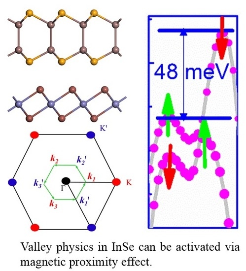
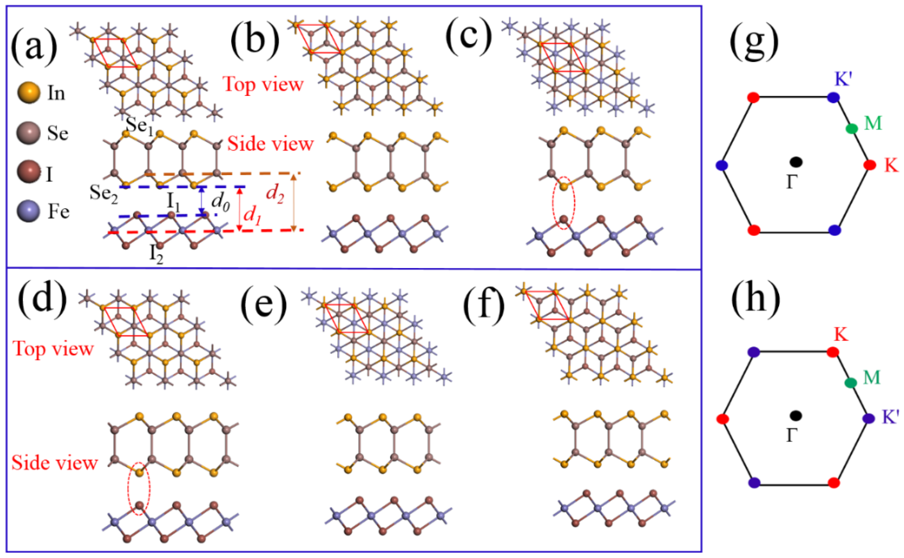
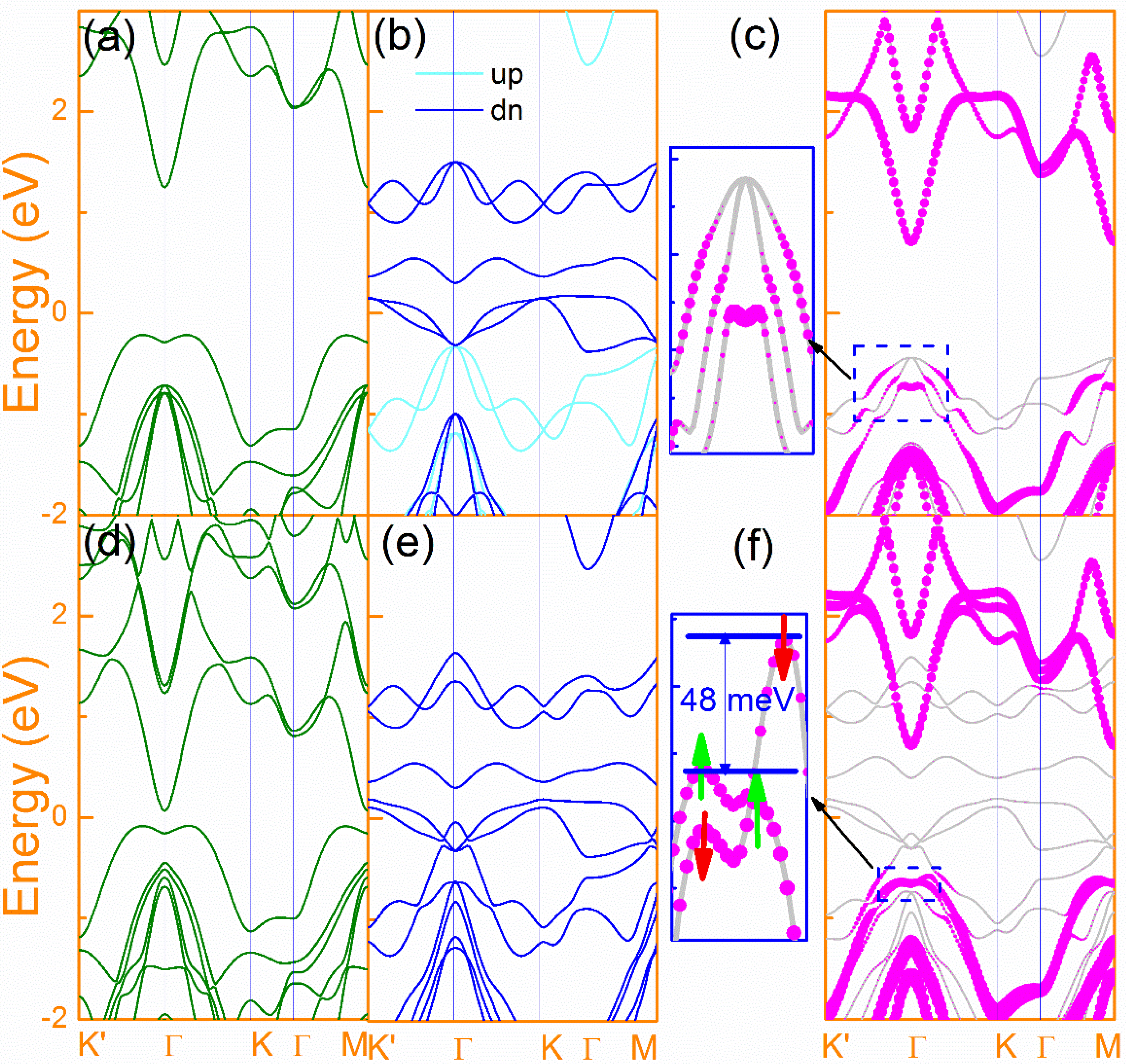
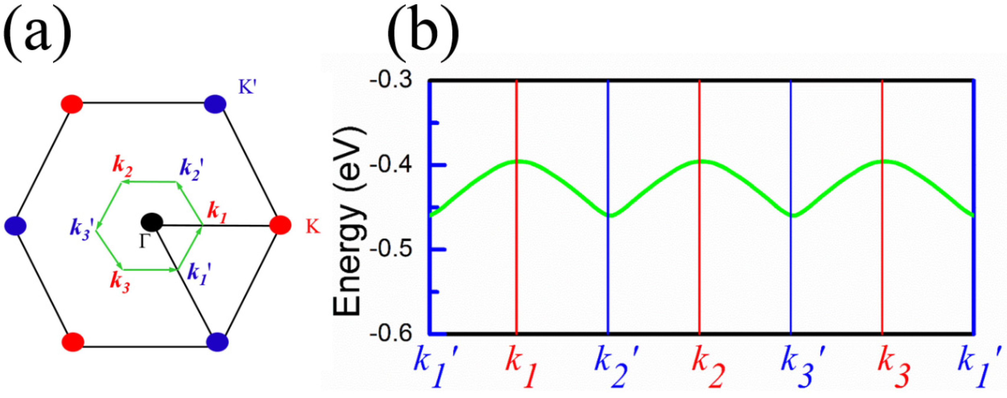
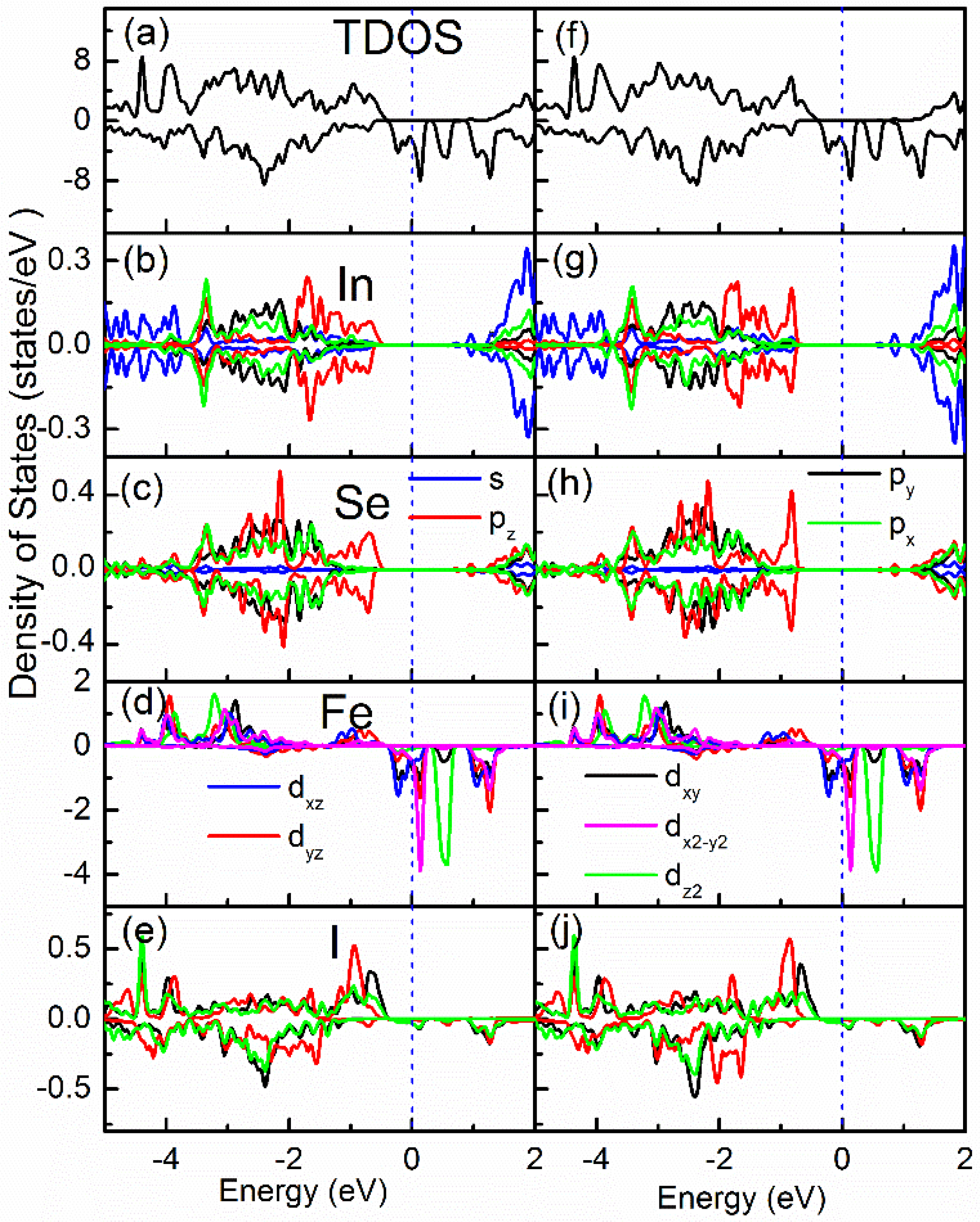
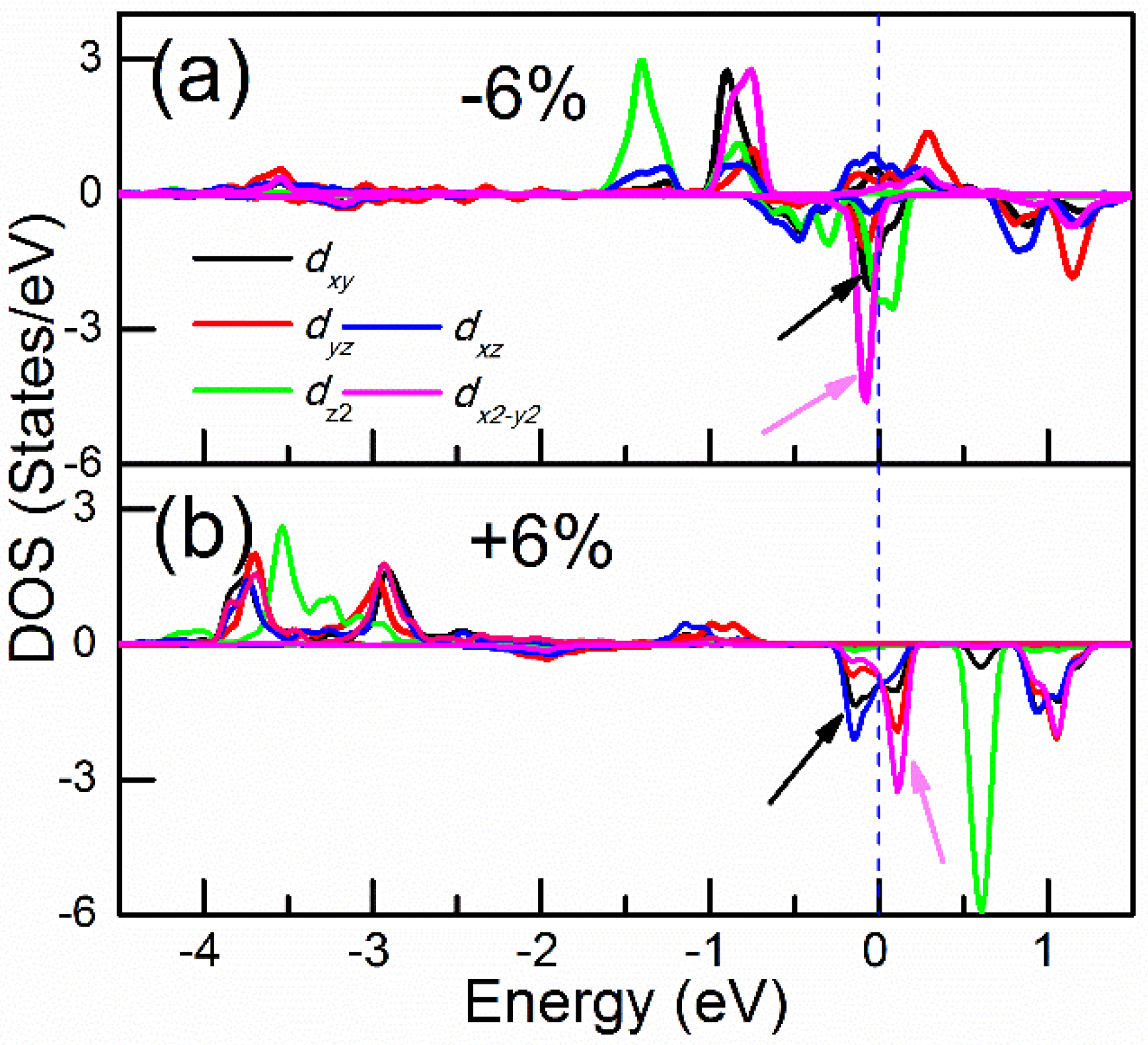
3.1. Electronic Structure
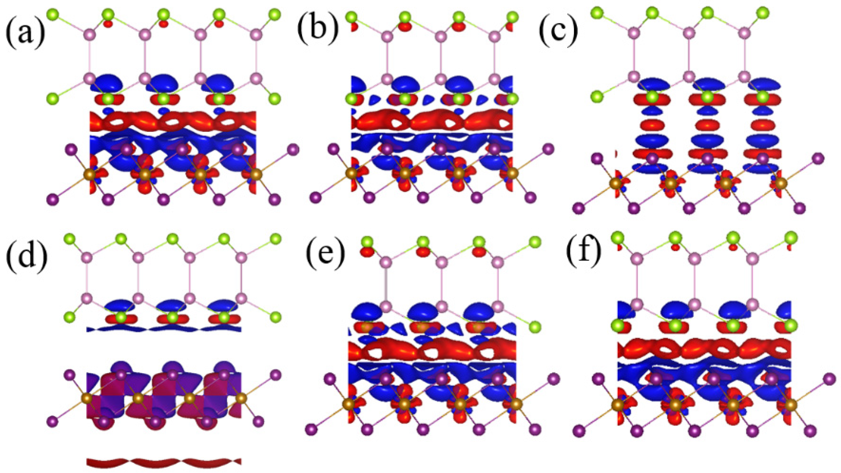
3.2. Interfacial Charge Transfer
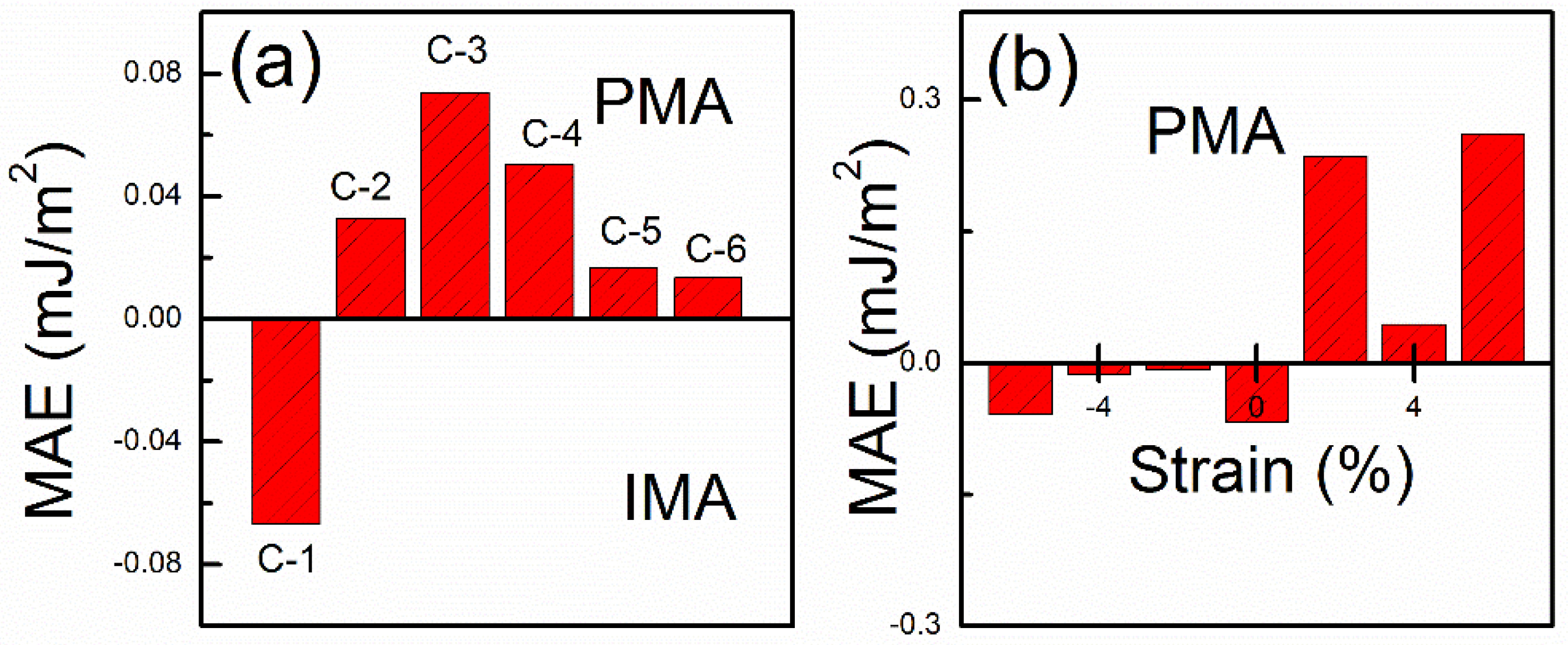
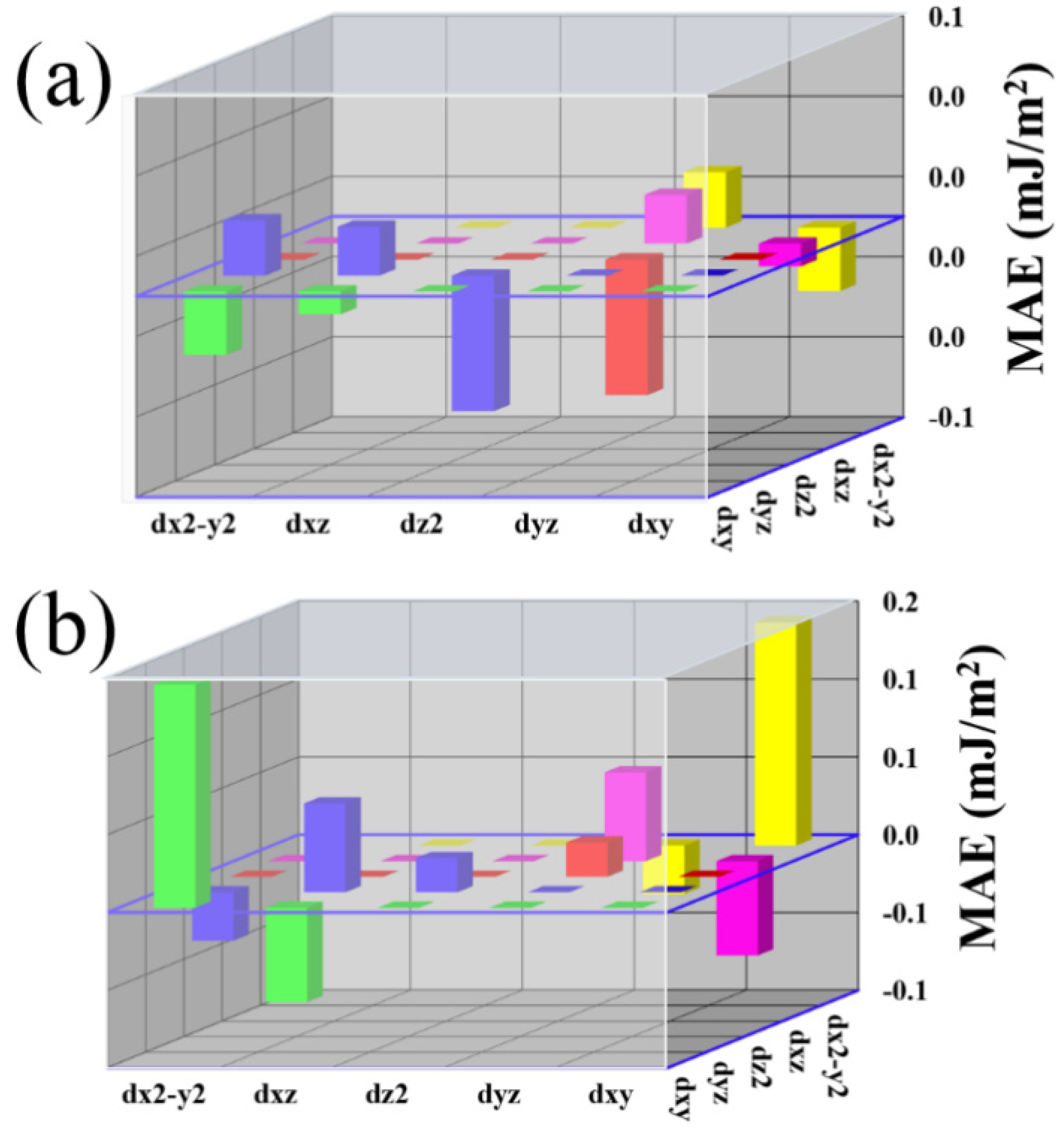
3.3. Magnetic Anisotropic Properties
4. Conclusions
Supplementary Materials
Author Contributions
Funding
Conflicts of Interest
References
- Novoselov, K.S.; Geim, A.K.; Morozov, S.V.; Jiang, D.; Zhang, Y.; Dubonos, S.V.; Grigorieva, I.V.; Firsov, A.A. Electric Field Effect in Atomically Thin Carbon Films. Science 2004, 306, 666–669. [Google Scholar] [CrossRef]
- Novoselov, K.S.; Jiang, D.; Schedin, F.; Booth, T.J.; Khotkevich, V.V.; Morozov, S.V.; Geim, A.K. Two-dimensional atomic crystals. Proc. Natl. Acad. Sci. USA 2005, 102, 10451–10453. [Google Scholar] [CrossRef]
- Mak, K.F.; Lee, C.; Hone, J.; Shan, J.; Heinz, T.F. Atomically Thin MoS2: A New Direct-Gap Semiconductor. Phys. Rev. Lett. 2010, 105, 136805. [Google Scholar] [CrossRef]
- Cao, T.; Wang, G.; Han, W.; Ye, H.; Zhu, C.; Shi, J.; Niu, Q.; Tan, P.; Wang, E.; Liu, B.; et al. Valley-selective circular dichroism of monolayer molybdenum disulphide. Nat. Commun. 2012, 3, 887. [Google Scholar] [CrossRef]
- Lee, Y.-H.; Zhang, X.-Q.; Zhang, W.; Chang, M.-T.; Lin, C.-T.; Chang, K.-D.; Yu, Y.-C.; Wang, J.T.-W.; Chang, C.-S.; Li, L.-J.; et al. Synthesis of Large-Area MoS2 Atomic Layers with Chemical Vapor Deposition. Adv. Mater. 2012, 24, 2320–2325. [Google Scholar] [CrossRef]
- Rodin, A.S.; Carvalho, A.; Castro Neto, A.H. Strain-Induced Gap Modification in Black Phosphorus. Phys. Rev. Lett. 2014, 112, 176801. [Google Scholar] [CrossRef]
- Li, L.K.; Yu, Y.J.; Ye, G.J.; Ge, Q.Q.; Ou, X.D.; Wu, H.; Feng, D.L.; Chen, X.H.; Zhang, Y.B. Black phosphorus field-effect transistors. Nat. Nanotechnol. 2014, 9, 372–377. [Google Scholar]
- Liu, H.; Neal, A.T.; Zhu, Z.; Luo, Z.; Xu, X.; Tománek, D.; Ye, P.D. Phosphorene: An Unexplored 2D Semiconductor with a High Hole Mobility. ACS Nano 2014, 8, 4033–4041. [Google Scholar] [CrossRef]
- Jiang, T.; Liu, H.; Huang, D.; Zhang, S.; Li, Y.; Gong, X.; Shen, Y.-R.; Liu, W.-T.; Wu, S. Valley and band structure engineering of folded MoS2 bilayers. Nat. Nanotechnol. 2014, 9, 825–829. [Google Scholar]
- Deng, Y.; Luo, Z.; Conrad, N.J.; Liu, H.; Gong, Y.; Najmaei, S.; Ajayan, P.M.; Lou, J.; Xu, X.; Ye, P.D. Black Phosphorus-Monolayer MoS2 van der Waals Heterojunction p-n Diode. ACS Nano 2014, 8, 8292–8299. [Google Scholar] [CrossRef]
- Fei, R.; Yang, L. Strain-Engineering the Anisotropic Electrical Conductance of Few-Layer Black Phosphorus. Nano Lett. 2014, 14, 2884–2889. [Google Scholar] [CrossRef]
- Qiao, J.; Kong, X.; Hu, Z.-X.; Yang, F.; Ji, W. High-mobility transport anisotropy and linear dichroism in few-layer black phosphorus. Nat. Commun. 2014, 5, 4475. [Google Scholar] [CrossRef]
- Xiao, D.; Liu, G.-B.; Feng, W.; Xu, X.; Yao, W. Coupled Spin and Valley Physics in Monolayers of MoS2 and Other Group-VI Dichalcogenides. Phys. Rev. Lett. 2012, 108, 196802. [Google Scholar] [CrossRef]
- Aivazian, G.; Gong, Z.; Jones, A.M.; Chu, R.-L.; Yan, J.; Mandrus, D.G.; Zhang, C.; Cobden, D.; Yao, W.; Xu, X. Magnetic control of valley pseudospin in monolayer WSe2. Nat. Phys. 2015, 11, 148–152. [Google Scholar] [CrossRef]
- MacNeill, D.; Heikes, C.; Mak, K.F.; Anderson, Z.; Kormányos, A.; Zólyomi, V.; Park, J.; Ralph, D.C. Breaking of Valley Degeneracy by Magnetic Field in Monolayer MoSe2. Phys. Rev. Lett. 2015, 114, 037401. [Google Scholar] [CrossRef]
- Li, Q.; Chen, K.-Q.; Tang, L.-M. Large Valley Splitting in van der Waals Heterostructures with Type-III Band Alignment. Phys. Rev. Appl. 2020, 13, 014064. [Google Scholar] [CrossRef]
- Zhang, Q.; Yang, S.A.; Mi, W.; Cheng, Y.; Schwingenschloegl, U. Large Spin-Valley Polarization in Monolayer MoTe2 on Top of EuO (111). Adv. Mater. 2016, 28, 959–966. [Google Scholar] [CrossRef]
- Liang, X.; Deng, L.; Huang, F.; Tang, T.; Wang, C.; Zhu, Y.; Qin, J.; Zhang, Y.; Peng, B.; Bi, L. The magnetic proximity effect and electrical field tunable valley degeneracy in MoS2/EuS van der Waals heterojunctions. Nanoscale 2017, 9, 9502–9509. [Google Scholar] [CrossRef]
- Yang, G.; Li, J.; Ma, H.; Yang, Y.; Li, C.; Mao, X.; Yin, F. Induced valley splitting in monolayer MoS2 by an antiferromagnetic insulating CoO(111) substrate. Phys. Rev. B 2018, 98, 235419. [Google Scholar] [CrossRef]
- Zhou, W.; Yang, Z.; Li, A.; Long, M.; Ouyang, F. Spin and valley splittings in Janus monolayer WSSe on a MnO(111) surface: Large effective Zeeman field and opening of a helical gap. Phys. Rev. B 2020, 101, 045113. [Google Scholar] [CrossRef]
- Xu, L.; Yang, M.; Shen, L.; Zhou, J.; Zhu, T.; Feng, Y.P. Large valley splitting in monolayer WS2 by proximity coupling to an insulating antiferromagnetic substrate. Phys. Rev. B 2018, 97, 041405. [Google Scholar] [CrossRef]
- Zhang, K.; Wang, L.; Wu, X. Spin polarization and tunable valley degeneracy in a MoS2 monolayer via proximity coupling to a Cr2O3 substrate. Nanoscale 2019, 11, 19536–19542. [Google Scholar] [CrossRef] [PubMed]
- Zhang, Z.; Ni, X.; Huang, H.; Hu, L.; Liu, F. Valley splitting in the van der Waals heterostructure WSe2/CrI3: The role of atom superposition. Phys. Rev. B 2019, 99, 115441. [Google Scholar] [CrossRef]
- Lin, C.; Li, Y.; Wei, Q.; Shen, Q.; Cheng, Y.; Huang, W. Enhanced Valley Splitting of Transition-Metal Dichalcogenide by Vacancies in Robust Ferromagnetic Insulating Chromium Trihalides. ACS Appl. Mater. Int. 2019, 11, 18858–18864. [Google Scholar] [CrossRef]
- Zhong, D.; Seyler, K.L.; Linpeng, X.; Cheng, R.; Sivadas, N.; Huang, B.; Schmidgall, E.; Taniguchi, T.; Watanabe, K.; McGuire, M.A.; et al. Van der Waals engineering of ferromagnetic semiconductor heterostructures for spin and valleytronics. Sci. Adv. 2017, 3, e1603113. [Google Scholar] [CrossRef]
- Nie, K.; Wang, X.; Mi, W. Magnetic proximity effect induced spin-dependent electronic structure in two-dimensional SnO by half-metallic monolayer CrN ferromagnet. Phys. Chem. Chem. Phys. 2019, 21, 6984–6990. [Google Scholar] [CrossRef]
- Ma, X.; Yin, L.; Zou, J.; Mi, W.; Wang, X. Strain-Tailored Valley Polarization and Magnetic Anisotropy in Two-Dimensional 2H-VS2/Cr2C Heterostructures. J. Phys. Chem. C 2019, 123, 17440–17448. [Google Scholar] [CrossRef]
- Bandurin, D.A.; Tyurnina, A.V.; Yu, G.L.; Mishchenko, A.; Zólyomi, V.; Morozov, S.V.; Kumar, R.K.; Gorbachev, R.V.; Kudrynskyi, Z.R.; Pezzini, S. High electron mobility quantum Hall effect and anomalous optical response in atomically thin InSe. Nat. Nanotechnol. 2016, 12, 223–227. [Google Scholar] [CrossRef]
- Knez, I.; Du, R.R.; Sullivan, G. Evidence for helical edge modes in inverted InAs/GaSb quantum wells. Phys. Rev. Lett. 2011, 107, 136603. [Google Scholar] [CrossRef]
- Xu, K.; Yin, L.; Huang, Y.; Shifa, T.A.; Chu, J.; Wang, F.; Cheng, R.; Wang, Z.; He, J. Synthesis, properties and applications of 2D layered MIIIXVI (M = Ga, In; X = S, Se, Te) materials. Nanoscale 2016, 8, 16802–16818. [Google Scholar] [CrossRef]
- Hu, P.; Wang, L.; Yoon, M.; Zhang, J.; Feng, W.; Wang, X.; Wen, Z.; Idrobo, J.C.; Miyamoto, Y.; Geohegan, D.B. Highly responsive ultrathin GaS nanosheet photodetectors on rigid and flexible substrates. Nano Lett. 2013, 13, 1649–1654. [Google Scholar] [CrossRef] [PubMed]
- Lei, S.; Ge, L.; Liu, Z.; Najmaei, S.; Shi, G.; You, G.; Lou, J.; Vajtai, R.; Ajayan, P.M. Synthesis and photoresponse of large GaSe atomic layers. Nano Lett. 2013, 13, 2777–2781. [Google Scholar] [CrossRef] [PubMed]
- Lei, S.; Wen, F.; Ge, L.; Najmaei, S.; George, A.; Gong, Y.; Gao, W.; Jin, Z.; Li, B.; Lou, J. An Atomically Layered InSe Avalanche Photodetector. Nano Lett. 2015, 15, 3048–3055. [Google Scholar] [CrossRef] [PubMed]
- Sucharitakul, S.; Goble, N.J.; Kumar, U.R.; Sankar, R.; Bogorad, Z.A.; Chou, F.-C.; Chen, Y.-T.; Gao, X.P.A. Intrinsic Electron Mobility Exceeding 103 cm2/(V s) in Multilayer InSe FETs. Nano Lett. 2015, 15, 3815–3819. [Google Scholar] [CrossRef] [PubMed]
- Radisavljevic, B.; Radenovic, A.; Brivio, J.; Giacometti, V.; Kis, A. Single-layer MoS2 transistors. Nat. Nanotechnol. 2011, 6, 147–150. [Google Scholar] [CrossRef]
- Ashton, M.; Gluhovic, D.; Sinnott, S.B.; Guo, J.; Stewart, D.A.; Hennig, R.G. Two-Dimensional Intrinsic Half-Metals With Large Spin Gaps. Nano Lett. 2017, 17, 5251–5257. [Google Scholar] [CrossRef] [PubMed]
- Zheng, H.; Zheng, J.; Wang, C.; Han, H.; Yan, Y. Enhancing the perpendicular magnetic anisotropy of 1T-FeCl2 monolayer by applying strain: first-principles study. J. Magn. Magn. Mater. 2017, 444, 184–189. [Google Scholar] [CrossRef]
- Magorrian, S.J.; Zólyomi, V.; Fal’ko, V.I. Spin-orbit coupling, optical transitions, and spin pumping in monolayer and few-layer InSe. Phys. Rev. B. 2017, 96, 195428. [Google Scholar] [CrossRef]
- Magorrian, S.J.; Zolyomi, V.; Fal’ko, V.I. Electronic and optical properties of two-dimensional InSe from a DFT-parametrized tight-binding model. Phys. Rev. B. 2016, 94, 245431. [Google Scholar] [CrossRef]
- Han, G.; Chen, Z.-G.; Drennan, J.; Zou, J. Indium Selenides: Structural Characteristics, Synthesis and Their Thermoelectric Performances. Small 2014, 10, 2747–2765. [Google Scholar] [CrossRef]
- Kresse, G.; Furthmuller, J. Efficient iterative schemes for ab initio total-energy calculations using a plane-wave basis set. Phys. Rev. B 1996, 54, 11169–11186. [Google Scholar] [CrossRef]
- Kresse, G.; Furthmüller, J. Efficiency of ab-initio total energy calculations for metals and semiconductors using a plane-wave basis set. Comput. Mater. Sci. 1996, 6, 15–50. [Google Scholar] [CrossRef]
- Blöchl, P.E. Projector augmented-wave method. Phys. Rev. B 1994, 50, 17953–17979. [Google Scholar] [CrossRef]
- Von Arnim, M.; Ahlrichs, R. Geometry optimization in generalized natural internal coordinates. J. Chem. Phys. 1999, 111, 9183–9190. [Google Scholar] [CrossRef]
- Allen, J.P.; Scanlon, D.O.; Parker, S.C.; Watson, G.W. Tin Monoxide: Structural Prediction from First Principles Calculations with van der Waals Corrections. J. Phys. Chem. C 2011, 115, 19916–19924. [Google Scholar] [CrossRef]
- Wang, D.-S.; Wu, R.; Freeman, A.J. First-principles theory of surface magnetocrystalline anisotropy and the diatomic-pair model. Phys. Rev. B 1993, 47, 14932–14947. [Google Scholar] [CrossRef]
- Zhu, Y.; Wang, X.; Mi, W. Tunable electronic structure and magnetic anisotropy of two dimensional van der Waals GeS/FeCl2 multiferroic heterostructures. J. Mater. Chem. C 2019, 7, 2049–2058. [Google Scholar] [CrossRef]
- Cheng, X.; Zhang, C.; Guan, L.; Tao, J. Origin of Intrinsic Direct Band Gap of Janus Group-III Chalcogenide Monolayers. Phys. Status Solidi B 2019, 256, 1900070. [Google Scholar] [CrossRef]
- Guan, L.; Cheng, X.; Tao, J. Strain effect on electronic structure of two-dimensional gamma-InSe nanosheets. Appl. Phys. Express 2017, 10, 125202. [Google Scholar] [CrossRef]
- Kanamori, J. Superexchange interaction and symmetry properties of electron orbitals. J. Phys. Chem. Solids 1959, 10, 87–98. [Google Scholar] [CrossRef]
- Takasuna, S.; Shiogai, J.; Matsuzaka, S.; Kohda, M.; Oyama, Y.; Nitta, J. Weak antilocalization induced by Rashba spin-orbit interaction in layered III-VI compound semiconductor GaSe thin films. Phys. Rev. B 2017, 96, 161303. [Google Scholar] [CrossRef]
- Li, P.; Appelbaum, I. Symmetry, distorted band structure, and spin-orbit coupling of group-III metal-monochalcogenide monolayers. Phys. Rev. B 2015, 92, 195129. [Google Scholar] [CrossRef]
- Ke, C.; Wu, Y.; Yang, W.; Wu, Z.; Zhang, C.; Li, X.; Kang, J. Large and controllable spin-valley splitting in two-dimensional WS2/h-VN heterostructure. Phys. Rev. B 2019, 100, 195435. [Google Scholar] [CrossRef]
- Yang, B.S.; Zhang, J.; Jiang, L.N.; Chen, W.Z.; Tang, P.; Zhang, X.G.; Yan, Y.; Han, X.F. Strain induced enhancement of perpendicular magnetic anisotropy in Co/graphene and Co/BN heterostructures. Phys. Rev. B 2017, 95, 174424. [Google Scholar] [CrossRef]


| C-1 | C-2 | C-3 | C-4 | C-5 | C-6 | |
|---|---|---|---|---|---|---|
| d0 (Å) | 3.227 | 3.288 | 3.949 | 3.950 | 3.259 | 3.261 |
| d1 (Å) | 4.808 | 4.872 | 5.538 | 5.5395 | 4.841 | 4.845 |
| d2 (Å) | 6.086 | 6.150 | 6.8195 | 6.820 | 6.119 | 6.122 |
| MFe (μB) | 3.37 | 3.373 | 3.374 | 3.375 | 3.371 | 3.372 |
| MI (μB) | 0.17 | 0.167 | 0.168 | 0.168 | 0.168 | 0.168 |
| MIn (μB) | 0.004 | 0.004 | 0.003 | 0.003 | 0.004 | 0.003 |
| MSe (μB) | 0.005 | 0.005 | 0.005 | 0.005 | 0.005 | 0.005 |
| ΔEf (meV) | 0 | 6 | 84 | 84 | 2 | 4 |
| ΔEv (meV) | 48.3 | 48.4 | 0.2 | 3.5 | 51.6 | 49.9 |
| o− | o+ | |||||||||
|---|---|---|---|---|---|---|---|---|---|---|
| u- | ||||||||||
| 0 | 0 | 0 | −1 | 4 | 0 | 0 | 0 | 1 | −4 | |
| 0 | 0 | −3 | 1 | −1 | 0 | 0 | 3 | −1 | 1 | |
| 0 | −3 | 0 | 0 | 0 | 0 | 3 | 0 | 0 | 0 | |
| −1 | 1 | 0 | 0 | 0 | 1 | −1 | 0 | 0 | 0 | |
| 4 | −1 | 0 | 0 | 0 | −4 | 1 | 0 | 0 | 0 | |
© 2020 by the authors. Licensee MDPI, Basel, Switzerland. This article is an open access article distributed under the terms and conditions of the Creative Commons Attribution (CC BY) license (http://creativecommons.org/licenses/by/4.0/).
Share and Cite
Lin, Y.; Zhang, C.; Guan, L.; Sun, Z.; Tao, J. The Magnetic Proximity Effect Induced Large Valley Splitting in 2D InSe/FeI2 Heterostructures. Nanomaterials 2020, 10, 1642. https://doi.org/10.3390/nano10091642
Lin Y, Zhang C, Guan L, Sun Z, Tao J. The Magnetic Proximity Effect Induced Large Valley Splitting in 2D InSe/FeI2 Heterostructures. Nanomaterials. 2020; 10(9):1642. https://doi.org/10.3390/nano10091642
Chicago/Turabian StyleLin, Yifeng, Changcheng Zhang, Lixiu Guan, Zhipeng Sun, and Junguang Tao. 2020. "The Magnetic Proximity Effect Induced Large Valley Splitting in 2D InSe/FeI2 Heterostructures" Nanomaterials 10, no. 9: 1642. https://doi.org/10.3390/nano10091642
APA StyleLin, Y., Zhang, C., Guan, L., Sun, Z., & Tao, J. (2020). The Magnetic Proximity Effect Induced Large Valley Splitting in 2D InSe/FeI2 Heterostructures. Nanomaterials, 10(9), 1642. https://doi.org/10.3390/nano10091642