3. Results
The spectroscopic ellipsometry technique allows the optical parameters of interest to be known by obtaining the change in the amplitude of the light after reflection (Ψ) and the phase change of this (Δ), through the mathematical inversion of the data (Ψ, Δ), which are converted directly into the optical constants refractive index (n) and extinction coefficient (k) [
21]. With the values n and k obtained by spectroscopic ellipsometry the transmittance and reflectance of all deposited SiO
x films were calculated by means of the reflection and transmission coefficients for the s and p polarizations which were calculated using Snell’s law [
22].
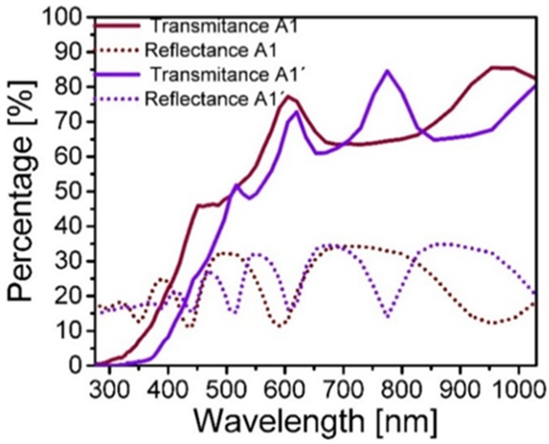
Figure 2 shows the reflectance and transmittance obtained specifically from A1 and A1’ SiO
x films. The transmittance and reflectance of the films A1 and A1’ are shown as a sample of the results obtained, however,
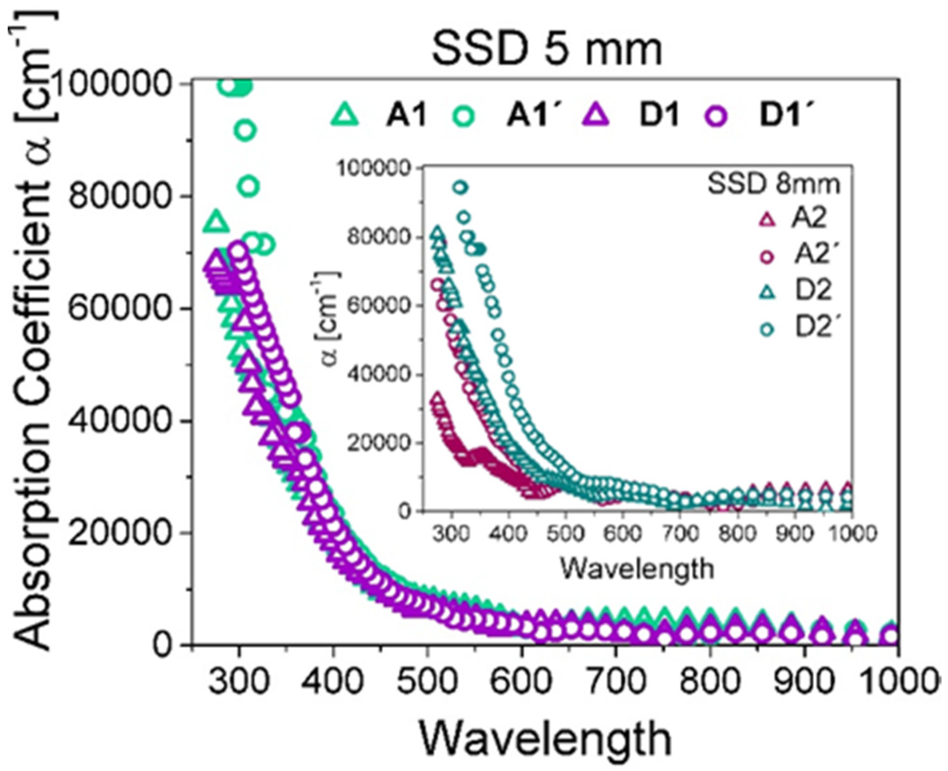
Figure 3 shows the complete results of the absorption coefficients obtained. In
Figure 2, transmittance less than 85% is observed and likewise reflectance less than 35%, in addition to the typical oscillations caused by the interference of the electromagnetic modes confined inside the films [
23]. On the other hand, to analyze deeply these results, the absorption coefficient α is calculated using the equations [
23]
which involve the values of reflectance and transmittance experimentally obtained. Since the specified transmittance and reflectance data have multiple interferences, obtaining the optical absorption coefficient is a process that may include a certain degree of error. For this reason, it is clarified that the values obtained are parameters that describe a particular sample and not the physical property.
The α results calculated for all deposited films are shown in
Figure 3, in which the inset shows the absorption coefficients of the films deposited at a higher sdd. From this figure it is observed that the absorption coefficient displays values which are similar to those reported in SiO
x films obtained using other methods of analysis, such as the transmittance obtained using UV-visible spectroscopy [
16]. It is worth noting that thermal annealed films increase their absorption coefficient and such a tendency prevails in all films, in addition to a slight increase in α for films deposited with a hydrogen flow level of 100 sccm. Such behavior results due to thermal effects provoke an atomic structural rearrangement which enriches the absorption mechanisms inside the material. Although this phenomenon has been previously reported in this material, it is still not well understood what type of arrangement occurs to increase the absorption coefficient when applying thermal annealing. It has been suggested that it may be due to the formation of ultra-small amorphous silicon grains that induce disorder in the network or due to the formation of nanocrystals since the optical properties of bulk and nanoscale materials differ [
24], or it has also been suggested that it may be due to an increase in the Si dangling bonds given the hydrogen desorption [
23] that is observed later. In the case of the present investigation, the three previously mentioned phenomena occur, for which all of them could contribute to the increase of the absorption coefficient. Theoretical studies have been carried out in other research works [
25] where the reactions that occur when applying thermal treatment are modeled.
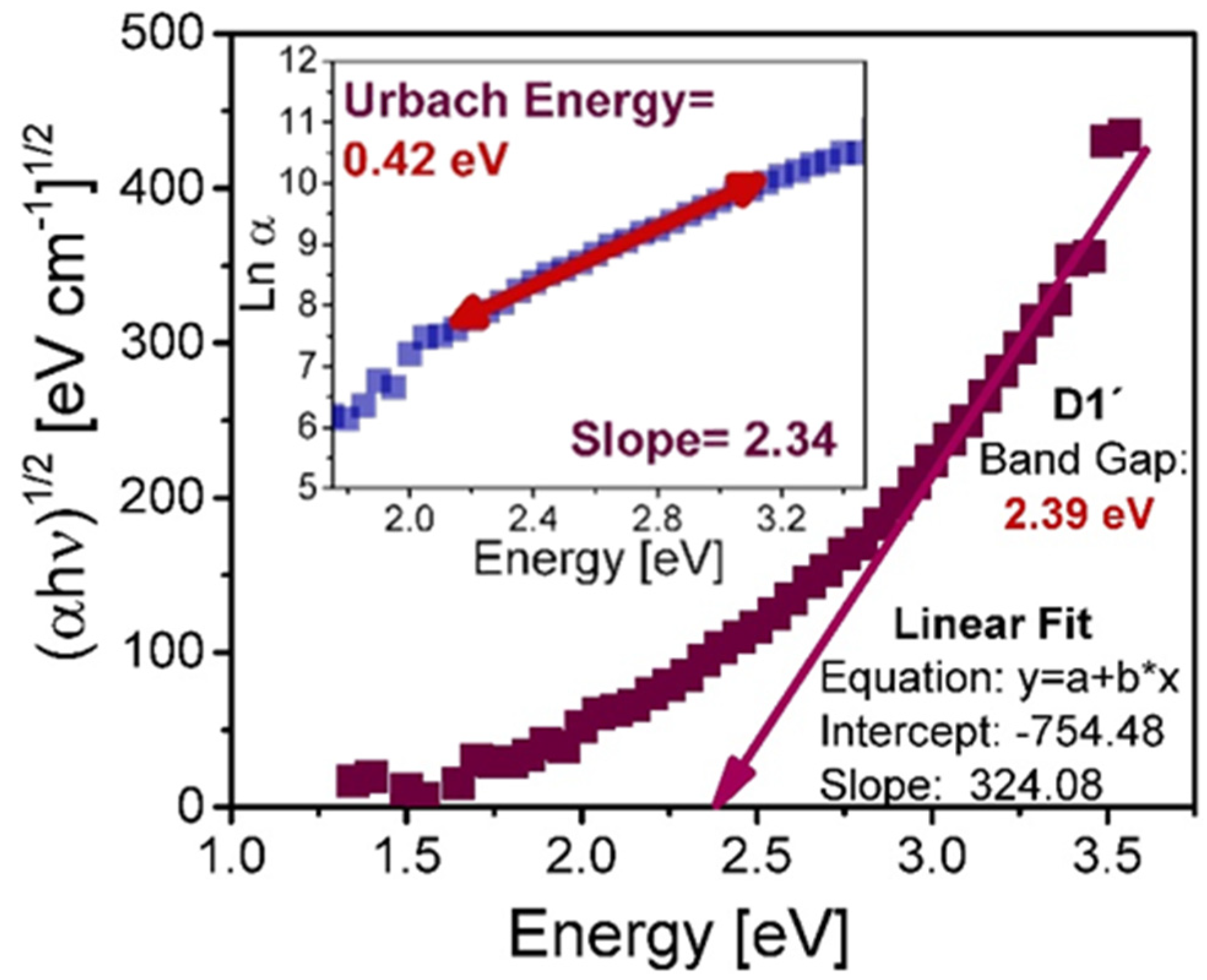
Using the values of the absorption coefficient (α), we estimate the band gap energy (BG) using the Tauc relation [
26] where the BG was obtained using linear regression considering the equation
where α is the absorption coefficient,
is the energy of the impinging photon,
is the BG, and A is an arbitrary constant. We also choose the exponent ½, which corresponds to an indirect allowed transition according to what other authors have used [
27,
28] for this material.
As is widely known, an amorphous material exhibits a complex structure of the density of states, such is the case for the SiO
x films. For this reason, the analysis of absorption mechanisms in this type of material is so complex; however, we can realize an approximation of the absorption coefficient through the presence of electronic states inside the band gap energy in the proximity of the valence and conduction band edges, as is proposed by the Urbach energies, which is now applied for the deposited SiO
x films using Urbach’s empirical rule, given by the equation [
29]
where α is the absorption coefficient,
is a constant, and
is Urbach’s energy, from (5) we obtain the following equation:
The Urbach energy (UE) can be obtained from the inverse slope of the straight line of the path versus energy of the incident photon.
Figure 4 shows an example of the procedure used to calculate the BG, while the inset in this figure shows the value of the corresponding UE for D1’ film. To obtain the BG, the linear region belonging to the high absorption edge was taken into account in such a way that in
Figure 4 it corresponds to energies from 3 eV to 3.5 eV, while to calculate the UE we utilize the energy region that is below the high absorption edge which corresponds to the energy range from 2.2 eV to 3 eV. This procedure is applied to each of the deposited films, and the results are displayed in
Table 2. From the results exhibited in
Table 2, it is remarkable that when we have a higher ssd in the deposit or a greater flow of hydrogen the value of BG energy increases and the UE decreases, a trend that is accomplished for all the films except for the D2 film, this could be due to the increase in the temperature of the substrate in the last seconds of deposit of the film D2, whereby there was a change in the deposit conditions, so the trend is not followed.
As can be seen, in general the thermal annealing increases the BG value and decreases the UE, which is an indication that a structural rearrangement occurs in the atomic lattice. Due to thermal effects such a phenomenon favors the crystallinity of the material. For that reason the UE is reduced, indicating that the amorphous phase is also reduced. This is corroborated using the FTIR technique.
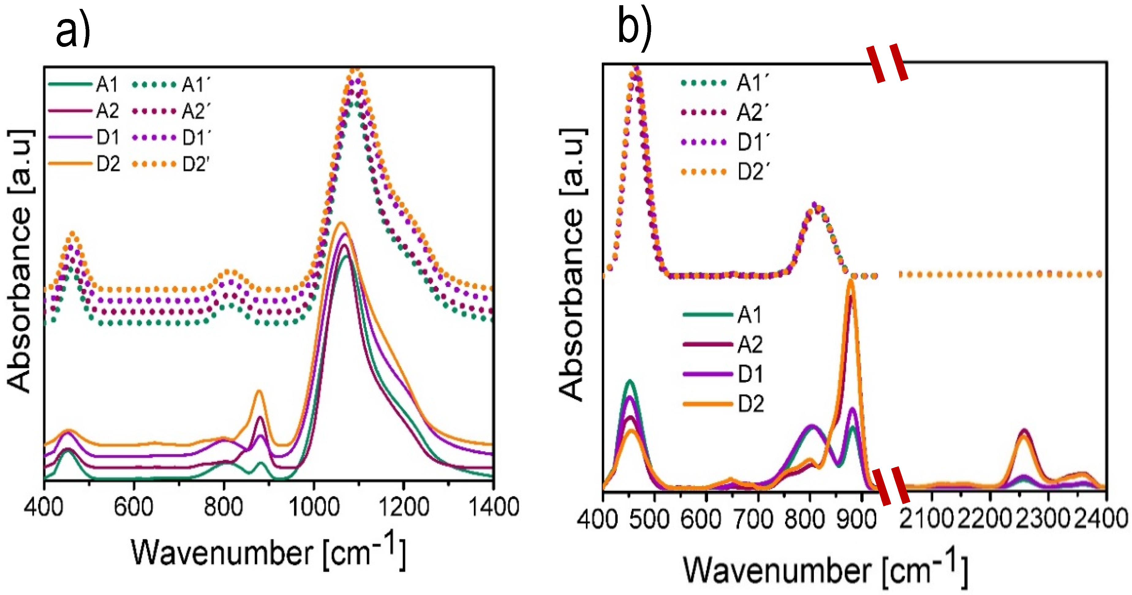
Figure 5a shows the FTIR spectra offset in the absorbance axis for all SiO
x films in a range from 400 cm
−1 to 1400 cm
−1. The solid lines correspond to the FTIR spectra of the films without thermal annealing and the dotted lines to the FTIR spectra with thermal annealing. By virtue of the intensity of the localized peak in the range from 950 cm
−1 to 1350 cm
−1, it is difficult to appreciate clearly both the shape and position of the peaks having less intensity. For this reason, in
Figure 5b) an amplification of the intensity of these peaks is shown by placing the spectra on a scale from 400 cm
−¹ to 950 cm
−¹ and from 2150 cm
−¹ to 2400 cm
−¹. All the spectra shown have been normalized with the purpose of not considering the variation of the thickness of the films and only taking into account the variations or shifts in wave number in the spectra.
In the obtained FTIR spectra, the characteristic absorption peaks of SiO
2 were identified. These peaks correspond to the vibration modes Si–O–Si rocking (R) at 458 cm
−1, Si–O–Si bending (B) at 812 cm
−1, and Si–O–Si stretching (S) at 1082 cm
−1 [
15]. There are shifts in the mentioned peaks indicating a stoichiometry different from that of SiO
2, which confirms the fact that the films are made up of SiO
x. The absorption peaks attributed to the Si–H bond were also found in the H–Si≡O
3 configuration, which are B at 880 cm
−1 and S at 2250 cm
−1; in addition, with a lower intensity absorption peaks attributed to the Si-H bond in the H–Si≡Si
3, H–Si≡O
2, H–Si≡O
1 configuration were found, which are S at 2100 cm
−1, 2156 cm
−1, and 2119 cm
−1, respectively. These configurations are reported in the literature [
29].
Table 3 shows the positions of the absorption peaks present in the deposited SiO
x films as well as the vibrational modes and the type of molecule to which they are attributed.
We can observe that, compared to the peak corresponding to the vibrational mode R of SiO2, the peak of the SiOx films without thermal annealing shows a slight shift towards lower wave numbers, this indicates a slight increase in silicon composition in some Si–O bonds, whereas with thermal annealing we have a condition closer to that of the SiO2 stoichiometry.
On the other hand, the peak located at 812 cm
−1 (Si–O–Si B) appears in all films; however, in films without thermal annealing, this peak is attached to the peak located at 880 cm
−1, which corresponds to the H–Si≡O
3 B molecule. This peak is closely related to the peak located at 2256 cm
−1 that corresponds to the vibrational mode S of the H–Si≡O
3 molecule. Having both vibrational modes in mind we corroborate the existence of the H–Si≡O
3 configuration in the films without thermal annealing, which is attributed to the hydrogen incorporation in the deposition process. In addition, a stronger intensity of these vibrational modes is observed for the films deposited at a larger ssd. It is also observed that when increasing the H–Si≡O
3 B peak the Si-O-Si R peak decreases, which is highly linked to the increase of silicon content in the material [
30]. After the film is annealed, both peaks disappear due to the desorption of hydrogen at high temperatures and the intensity of the Si–O–Si B mode increases, which is, as already mentioned, characteristic of SiO
2.
The peak corresponding to the vibrational mode S provides information about the composition of the deposited films. When this peak displaces towards higher wave number values it indicates that the density of the Si–O–Si bonds is increased, and such films are more stoichiometric [
31]. In films without thermal annealing, the peak assigned to the vibrational mode of stretching is shifted towards smaller wave numbers, suggesting a higher proportion of silicon in the amorphous phase and a greater amount of unbound oxidation states. However, when applying thermal annealing, the peak goes towards larger wave numbers, which indicates an increase in the Si–O–Si bonds; therefore, the oxygen bonds are also increased and it indicates a change in the silicon excess, this makes the stoichiometry of the films closer to that of the SiO
2 films.
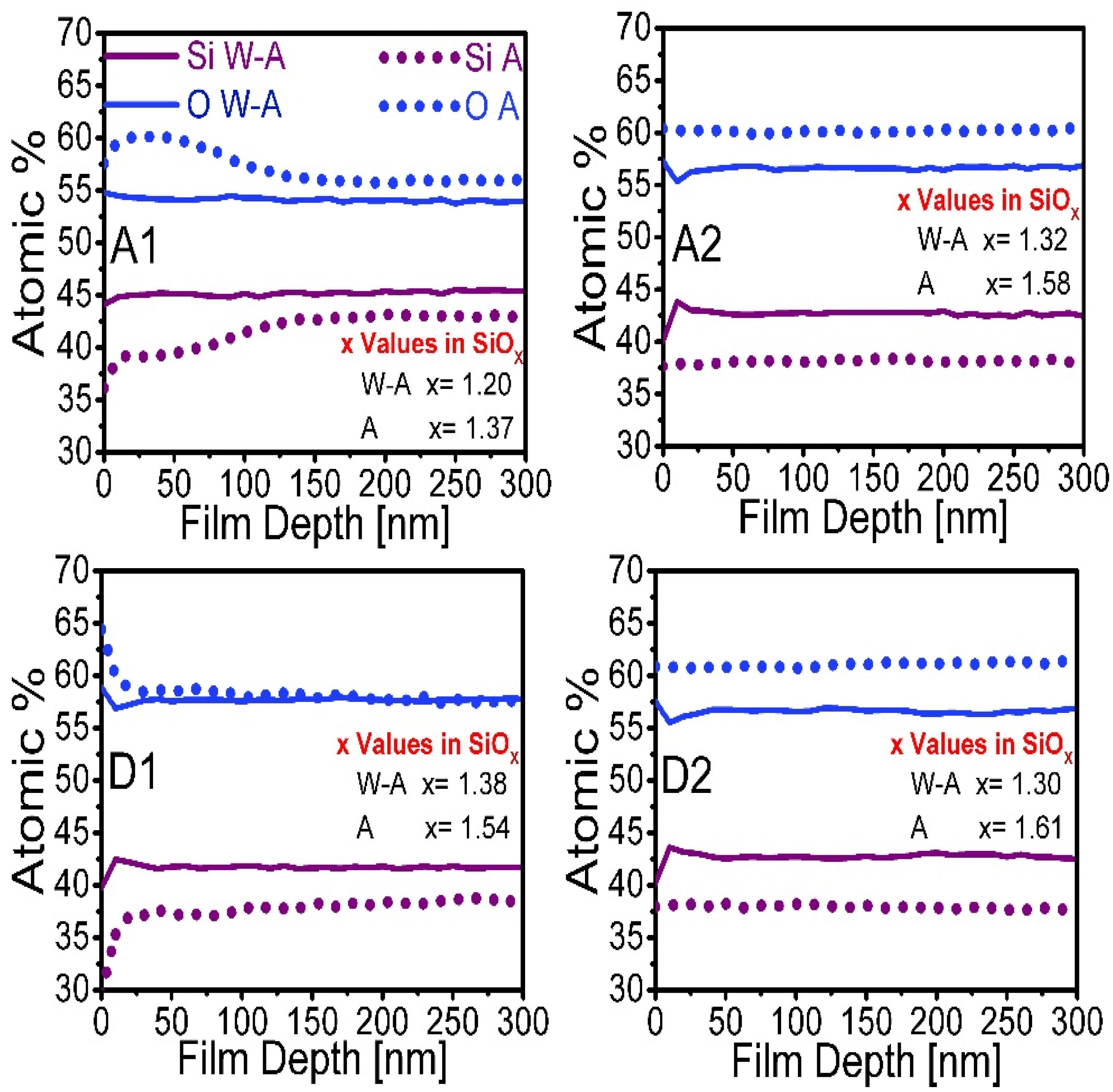
The XPS technique allows information to be obtained on the binding energy of the elements present in a material. From the XPS measurements, the oxygen and silicon composition of the SiOx films and the oxidation states Sin+ present were obtained.
Figure 6 shows the composition profile in percentage of silicon and oxygen of the films according to the depth of penetration, where dotted line curves are shown for annealed films, while the continuous lines represent films without thermal annealing. With this data it was possible to obtain an average value of x in the stoichiometric SiO
x ratio for each of the films using the formula
ratio [
32].
In
Figure 6, a remarkable change is observed in the amount of silicon and oxygen present in the proximity of the film surface with respect to that present inside the volume. Such change is more remarkable for films with thermal annealing. Particularly for the A1 and D2 films, the change is more abrupt. Such films were deposited at a lower ssd; in addition, for these samples the annealing effect enhanced the stoichiometry in the region near the surface due to both the atomic rearrangement and the increment of oxygen atoms. The x values show that in general thermal annealing films present an increase in x, which indicates an increase in the amount of oxygen and a tendency towards SiO
2 stoichiometry.
To obtain the oxidation states of silicon Si
n+ (with n = 1, 2, 3, 4) corresponding to the chemical structures Si–OSi
3, Si–O
2Si
2, Si–O
3Si, and Si-O
4, respectively [
33], as well as the chemical state of silicon in bulk Si0 (Si2p3/2 and Si2p1/2), the XPS spectra of the Si2p peak were deconvolved to find the corresponding binding energies attributed to each of the previous states. These energies are shown in
Table 4 [
33].
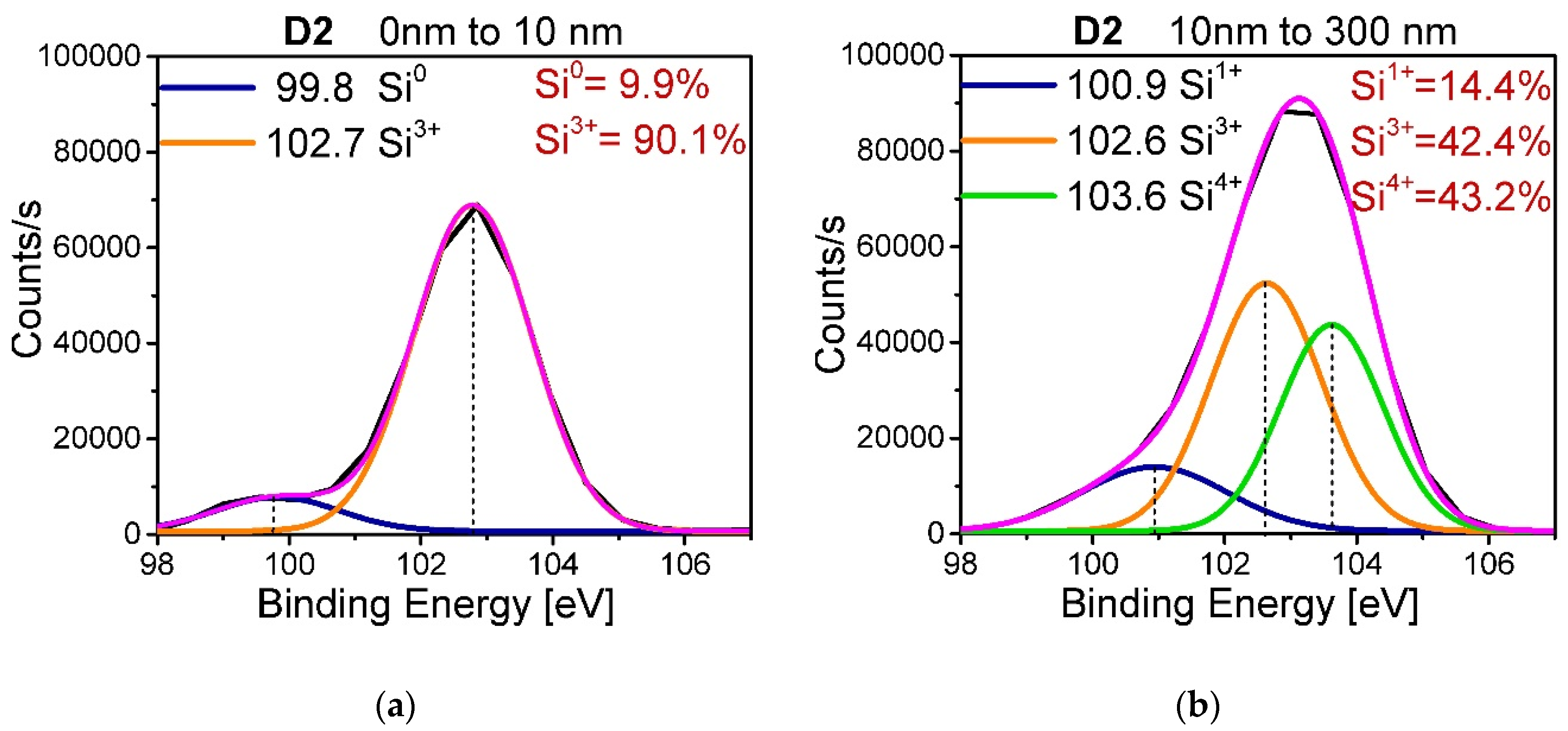
As an example, in
Figure 7 the deconvolution of the spectrum corresponding to the D2 film is shown (a) on the surface of the film (0 to 10 nm) and (b) in the volume of the film (10 nm to 300 nm).
The relative concentration in percentage of each oxidation state (I) can be obtained using Equation (7) [
33]:
where
is the area of the peak that represents the oxidation state Si
n+, and
is the total area of the Si2p peak. In
Figure 7 it can be seen that for the surface part of the film the binding energies present are attributed to the oxidation states of Si
0 and Si
3+, with percentages of 9.9% and 90.1%, respectively, while in volume the Si–Si bonds disappear and the oxidation states Si
1+, Si
3+, and Si
4+ remain, with percentages of 14.4%, 42.4%, and 43.2%, respectively.
The above process was carried out for all the spectra on the surface of the film (10 nm), in the center of the film at a depth of 60 nm, and finally at a depth of 300 nm. The results are shown in
Table 5, together with the respective oxidation state attributed to that binding energy.
From
Table 5 it is observed that films without thermal annealing present Si
0 states generally on the surface of the film, except for the A1 film that shows it only in volume, this being also the one with the highest silicon content. Comparing the films according to the ssd of the deposit, films deposited at greater ssd without thermal annealing show the oxidation states Si
0 and Si
3+ on the surface of the film, while in volume they have oxidation states Si
1+, Si
3+, and Si
4+. When applying thermal annealing to these films the oxidation states are reduced to Si
3+ and Si
4+, both for the surface of the film and for the volume; that is, the stoichiometry of the films is closer to that of the SiO
2 and the films tend to become uniform in their stoichiometry, in addition the film deposited to greater flow D2’, has a higher percentage of Si
4+ oxidation state than that deposited at 25 sccm (A2’).
As for the films deposited at lower ssd without thermal annealing, the oxidation state Si1+ is absent while the oxidation state Si2+ is only present in volume and Si3+ is only present on the surface of the sample with lower flux level (25 sccm), but it exists both on the surface and in volume for the sample with a higher flux level (100 sccm), and Si4+ exists for both space regions in the two samples. Additionally, the films show significant changes in the percentages of oxidation states only in the most superficial layer. On the other hand, the relevant characteristic of the annealed films is that they present the oxidation states Si3+ and Si4+ in both space regions; however, the oxidation states Si0 and Si2+ are absent. The oxidation state Si1+ exists on the surface of both samples and in volume but at different depths.
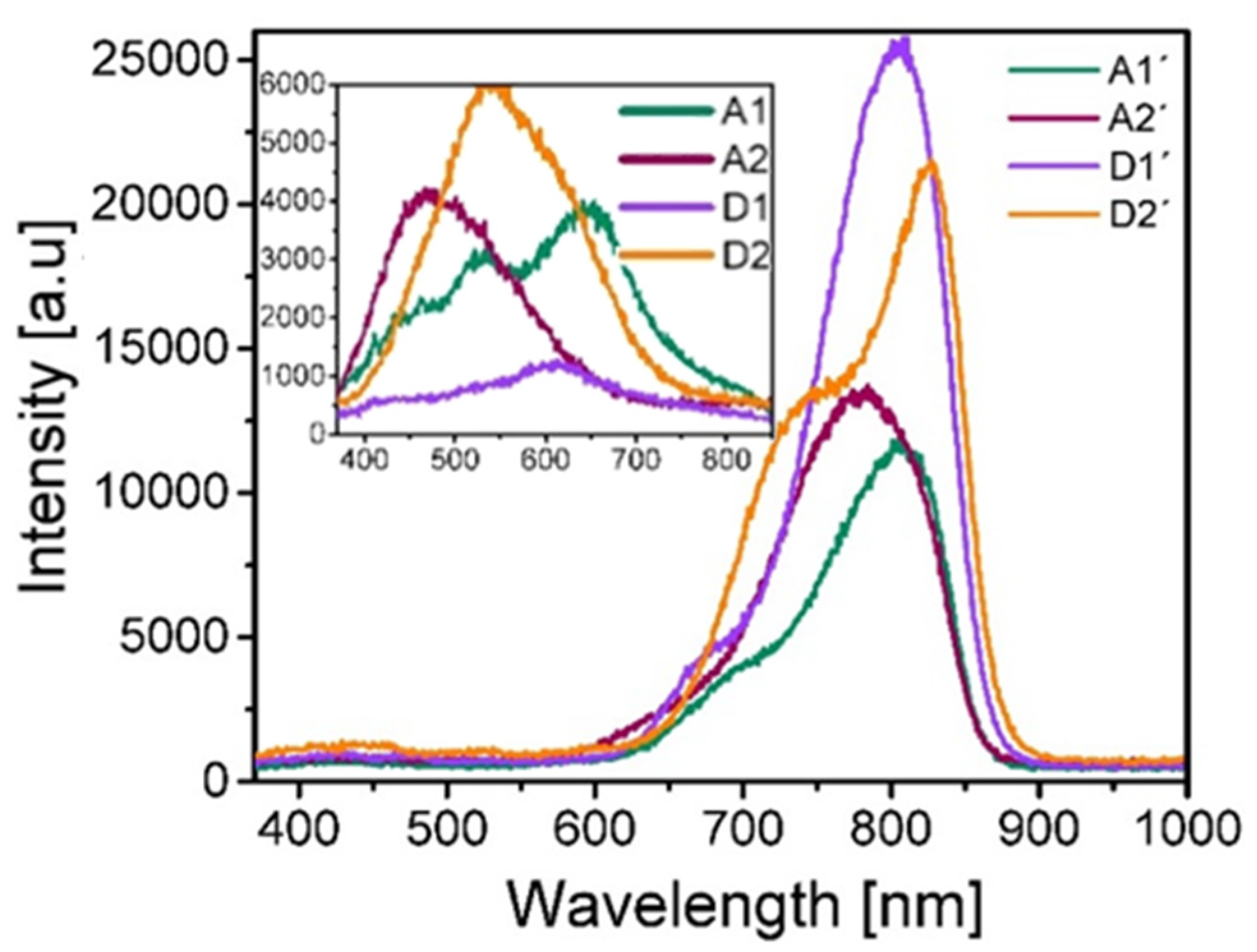
Once the molecular bonds present in the material were identified using the FTIR technique, in addition to the oxidation states being quantified using XPS, it was also necessary to know the structural defects in the SiOx films, for which photoluminescence (PL) measurements were carried out.
The results obtained of such PL measurements are shown in
Figure 8, where the inset in the graph depicts the spectra obtained from the films without thermal annealing, while the main graph shows the PL spectra obtained from the annealed films. It is worth noting that the PL intensity from all films with thermal annealing is augmented approximately up to 4 times with respect to that of the films without thermal annealing. Additionally, such spectra undergo a shift in the emission wavelength towards lower energies in such a way that PL intensity lies in the range 650–900 nm. It should be noted that the strongest PL intensity corresponds to the annealed films deposited at a flow level of 100 sccm, while for films without thermal annealing it corresponds to the films deposited at flow levels of 100 sccm and 25 sccm, and the emission region is wider, in the range 400–800 nm. It is noticeable that all the emission PL bands are wide, which indicates that they are composed of several emission peaks that have a shape similar to a Gaussian one.
For SiO
x, the most accepted light emission mechanisms which give rise to the visible and near infrared bands are attributed to the following causes: the effect of dimensional quantum confinement in Si-ncs or silicon nanoclusters (Si-ncl) whose reported photoluminescence lies in the emission energy range from 1.3 eV to 1.7 eV [
34,
35,
36] and the effect related to defects in the oxide matrix such as weak oxygen bonds (WOB) with a PL peak at 3 eV [
36], neutral oxygen vacancy (NOV) with PL ranging from 2.8 eV to 2.9 eV [
37], hydrogen-related defects (H) with PL located in the range from 2.2 eV to 2.5 eV [
38], and finally a non-bridging oxygen hole center (NBOHC) with PL from 1.8 eV to 2 eV [
39,
40]. These emission mechanisms make the PL spectra exhibit a wide shape, as can be seen in
Figure 8. In order to find all possible contributions to the photoluminescent processes in the SiO
x films, the deconvolution of each spectrum was performed, by way of example.
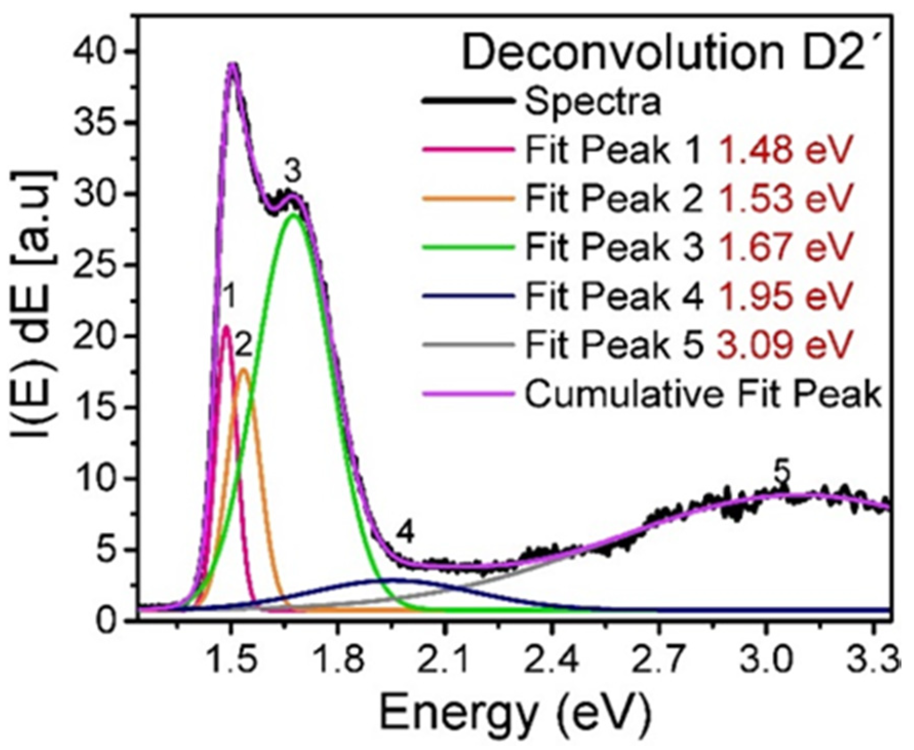
Figure 9 depicts the deconvolution of the photoluminescent spectrum of the D2’ film. To perform the deconvolution and in order to avoid common errors reported in the photoluminescence analysis, the spectra were deconvolved using the PL intensity-energy differential versus energy [
41].
Table 6 shows the position of the peaks obtained from the deconvolution of the photoluminescent spectra, in addition to the defects to which the emission is attributed, according to their energy position.
As can be seen in
Table 6, films without thermal annealing show photoluminescence attributed to NOV and H, in addition to films deposited at a shorter ssd showing the presence of NBOHC, while those deposited at a larger ssd have WOB. For annealed films, photoluminescence is mainly due to Si-ncl effects and to a lesser extent to NBOHC and WOB defects.
4. Discussion
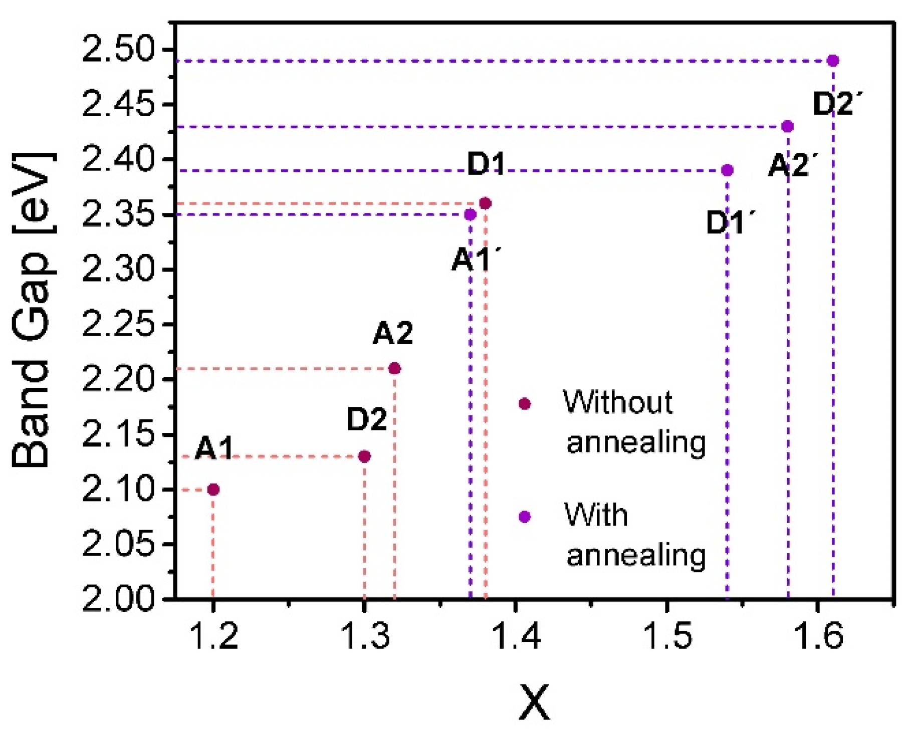
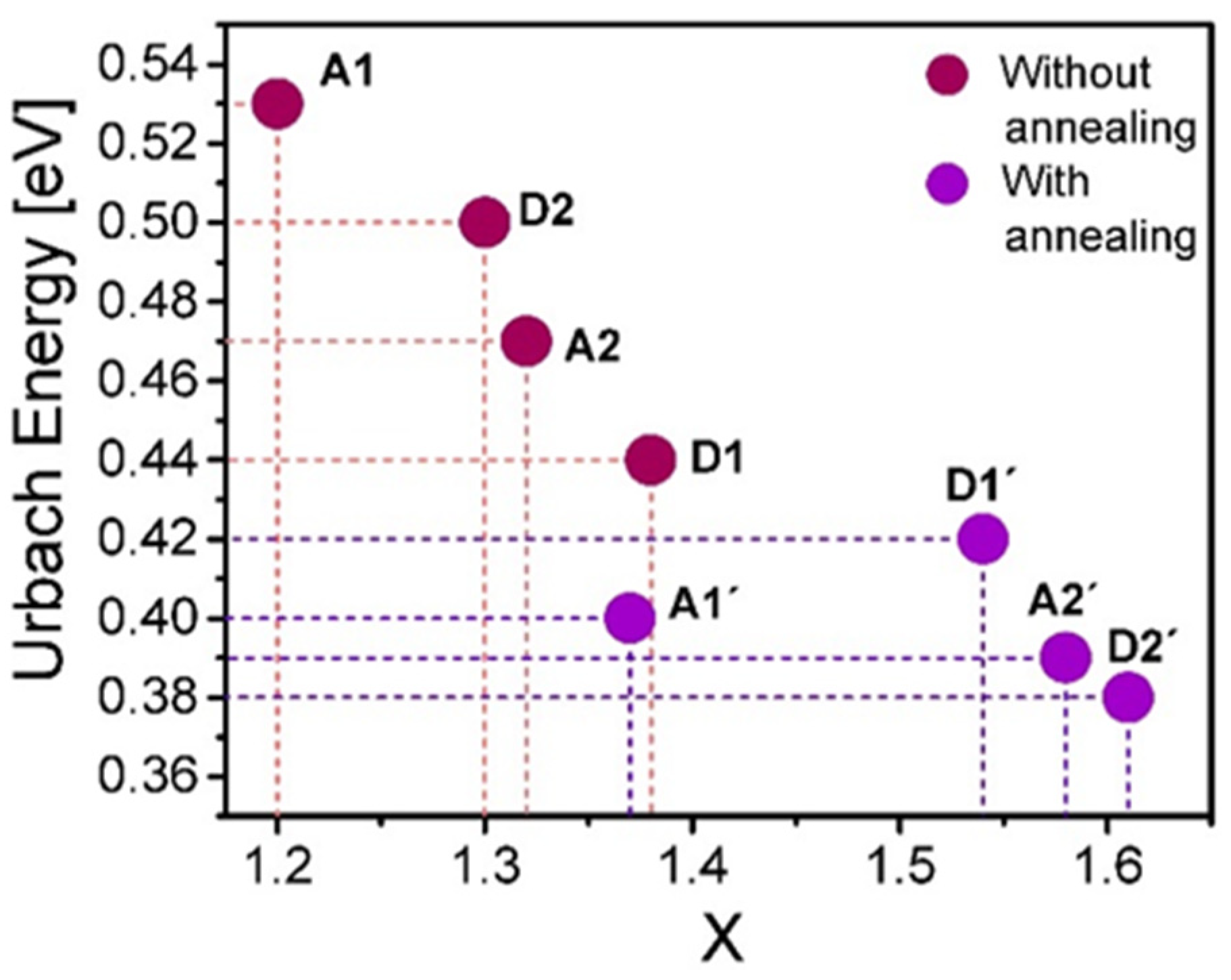
Using the calculated values of the BG, the UE parameters, and making a correlation with the results obtained using XPS, we identify a clear dependence between the stoichiometric ratio (x) and the BG and UE values.
Figure 10 and
Figure 11 display how the correlation between the stoichiometric ratio and BG and UE evolves.
Figure 10 shows a clear tendency in films in which with a higher silicon or lower oxygen content (lower value of x) the lower BG is obtained. Such a trend is held both with and without annealing, and it is relevant to point out that the BG increases significantly due to both thermal annealing and the increase of oxygen content. In addition, the UE decreases monotonously in accordance with the silicon content decreasing with the thermal annealing, as is shown in
Figure 11. Special attention deserves to be paid to the fact that the annealed films with the larger ssd and higher flow level offer the highest BG and stoichiometric ratio and the lowest UE.
The calculated Urbach energies occupy a wide range of values ranging from 380 meV to 530 meV. These are considerable energy values, and it indicates in some way the level of structural disorder that exists in the SiO
x films. This disorder is remarkably diminished both with the oxygen increment and with the thermal annealing. In addition to that the dependence among the stoichiometric ratio, band gap and Urbach energies is well defined and agrees with the model established by Mott [
31]. For values of the stoichiometry ratio x further from that of the stable configuration of silicon dioxide, the films undergo a greater disorder in the molecular structure of the material, which brings the increment of aggregate energy levels inside the intrinsic band gap energy of the dioxide matrix, causing the formation of wider band tails and consequently a smaller band gap energy that tends towards that of the silicon one.
Comparing these results with the deposition parameters, we find a behavior in which, with a lower flow level and shorter ssd, films with a higher silicon content (lower BG and higher UE) are obtained, and therefore, the optical response of the material is substantially modified. It is worthwhile to note that the trend in which the flow level and ssd determine the dependence between the silicon content and BG and UE is not well defined for the case of the films without thermal annealing, contrary to the case of the annealed films for which the increment of the ssd and flow level diminish the silicon content and increase the BG and reduce the UE clearly. Furthermore, for the films without thermal annealing, the presence of hydrogen is observed in the FTIR spectra of these films (see
Figure 12), which suggests that hydrogen plays an important role which causes a clear dependence between the silicon content and the GB and UE parameters not to exist, as in the case of the annealed films in which hydrogen is no longer present.
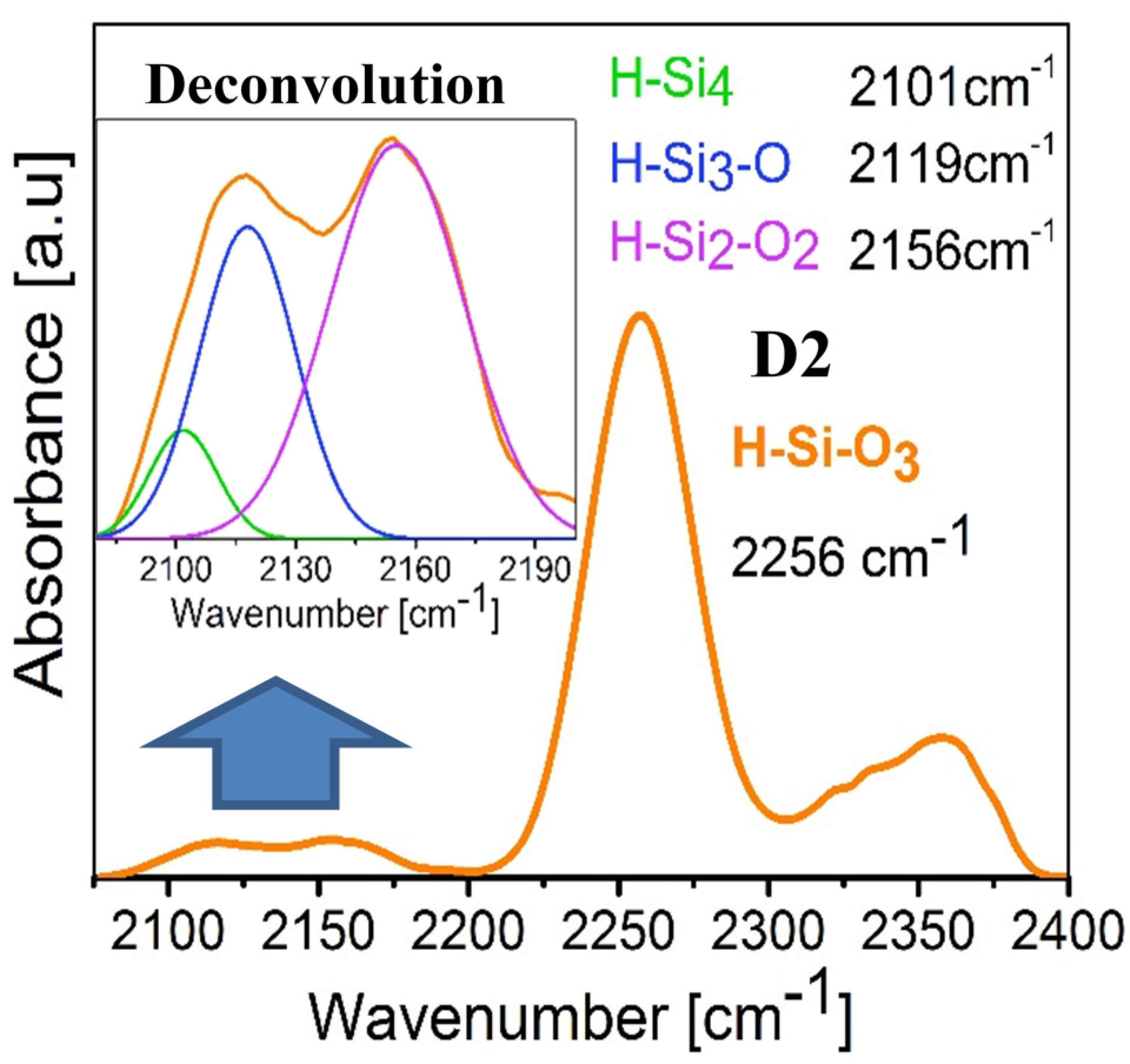
Figure 12 shows an amplification of the IR spectrum in the region from 2100 cm
−1 to 2400 cm
−1 for the D2 film; in addition, the deconvolution made from the 2075 cm
−1 peak to the 2150 cm
−1 one is shown. Such deconvolutions were performed to observe the absorption peaks attributed to the Si–H bonds in the H–Si≡Si
3, H–Si≡O
2 and H–Si≡O
1 configurations, while
Table 7 lists the peak positions for all films without thermal annealing, which are the ones that present the Si–H bonds.
Figure 12 shows the presence of the H–Si≡Si
3, H–Si≡O
2, and H–Si≡O
1 configurations, whose contributions are minimal compared to the one due to the H–Si≡O
3 configuration, which is found at position 2256 cm
−1 and shows a significant right shoulder which is ascribed to an effect of the first neighbors with silicon atoms [
30]. When comparing these results with those obtained using XPS, where it is observed that the predominant oxidation states are Si
3+ and Si
4+, t is then confirmed that an important part of these Si≡O
3 bonds are bound to hydrogen atoms.
Regarding the hydrogen content in the films without thermal annealing, it is greater for films deposited at a larger ssd. This is explained by indicating that a greater deposit distance leads to the formation of weak silicon-silicon or silicon-oxygen bonds. These bonds, as it is well known, are broken by the action of hydrogen forming covalent bonds Si–H, which explains the presence of the H–Si≡O3, H–Si≡Si3, H–Si≡O2, and H–Si≡O1 configurations in the FTIR spectra.
The results obtained using PL are used in the analysis of the formation of defects in the SiOx films; however, it is hitherto the most controversial and difficult topic without conclusive reasons. In the case of the results obtained for films deposited without thermal annealing, the abovementioned result is shown regarding the presence of weak oxygen bonds, which are shown for films deposited at a greater ssd. Neutral oxygen vacancies are present for all films without thermal annealing, which is common for this type of material.
The emission related to defects involving hydrogen is more evident for films deposited at a larger ssd (A2, D2). In the case of NOVs, it is known that they react with hydrogen to form H–Si≡ configurations, so it is interesting to note that this defect is only present in films without thermal annealing. It is very probable that films without annealing have converted a part of their NOVs into H–Si≡O3 configurations.
Since the films without thermal annealing deposited at a shorter ssd have a higher silicon content and oxidation states Si0 with respect to the other films, we expect that the emission at 1.9 eV is not mostly due to NBOHC defects that are closely related to the SiO4, but to another type of defect which is also reported with this characteristic emission, interstitial oxygen (), which would be more appropriate since NBOHC is not present in the A2 and D2 films that have a greater amount of Si4+ oxidation states; however, it is not discarded that it is a contribution of both emission mechanisms.
In the case of PL in annealing films, they all show the same emission mechanisms, attributed to WOB, NBOHC, and the greater contribution to PL is attributed to Si-ncl effects, which brings confinement effects due to a nanocrystal formation producing an increase of the band gap, which is controlled by the Si nanostructure size [
42]; however, it is believed that there is a better explanation for this purpose, which will be discussed later, in addition to the fact that emission intensity increases substantially compared to that of films without thermal annealing, which indicates that the structural rearrangement of the material is closely related to this reported emission. To understand how the material restructuring occurs, we take into account the results obtained from the deconvolution of the Si2p peak, as mentioned by Tomozeiu [
31]. Based on the Gibbs free energy calculations, it has been shown that the bonds Si-(Si
4) and Si-(O
4) are stable, while the Si-(Si
nO
4−n) bonds, with n = 1, 2, 3 are unstable, being Si-(Si
2O
2), which corresponds to a state of Si
2+ oxidation, the less stable structural entity. The films deposited at an ssd of 5 mm without thermal annealing present this oxidation state, which leads to a greater tension or stress of the chemical bond between the central silicon atom and the oxygen ones, so if the conditions for the migration of an oxygen atom are satisfied, a phase decomposition will occur following the next reaction:
The first reaction is observed according to the oxidation states present when applying thermal annealing to these films (Si
1+ and Si
3+). However, in the films deposited at a larger ssd, the states Si
1+ and Si
3+ are already present in the films without thermal annealing, indicating that the deposition of the film under this condition leads to a more stable lattice growth that could be favored as the results of FTIR indicate. Due to the incorporation of hydrogen and the formation of a greater amount of H–Si≡O
3 bonds, where hydrogen helps to reduce tension in the molecular structure, the presence of hydrogen could be inferred not only using this technique, but could also be considered through the photoluminescent emission band (2.2 eV to 2.5 eV) attributed to defects related to hydrogen [
40]. When applying thermal annealing to these films as observed using FTIR, a hydrogen desorption occurs so that the H–Si≡O
3 bond can become a Si-(SiO
3) bond with the addition of a silicon atom. It can be observed in
Table 6 that when the films were annealed, only the oxidation states Si
3+ and Si
4+ survived, and such states are present in the A2’ and D2’ films that have a stoichiometry closer to that of SiO
2 and a major BG and a smaller UE.
As previously mentioned, reports that exist regarding the structural arrangements that are presented when thermal annealing is performing in this type of films suggest, given the stoichiometry, the formation of isolated nanoclusters or nanocrystals of silicon immersed in a SiO
2 matrix, instead of an arrangement of the type of percolated networks or Si-SiO
2 sponges that are formed when there is an excess of Si greater than 30% [
20,
43]. One method to characterize these silicon nanocrystals or nanoclusters is through the XRD technique; however, a difficulty has been reported in obtaining a diffraction pattern for very small Si nanocrystals dispersed in the amorphous SiO
x matrix due to the fact that they have a short-range crystalline order [
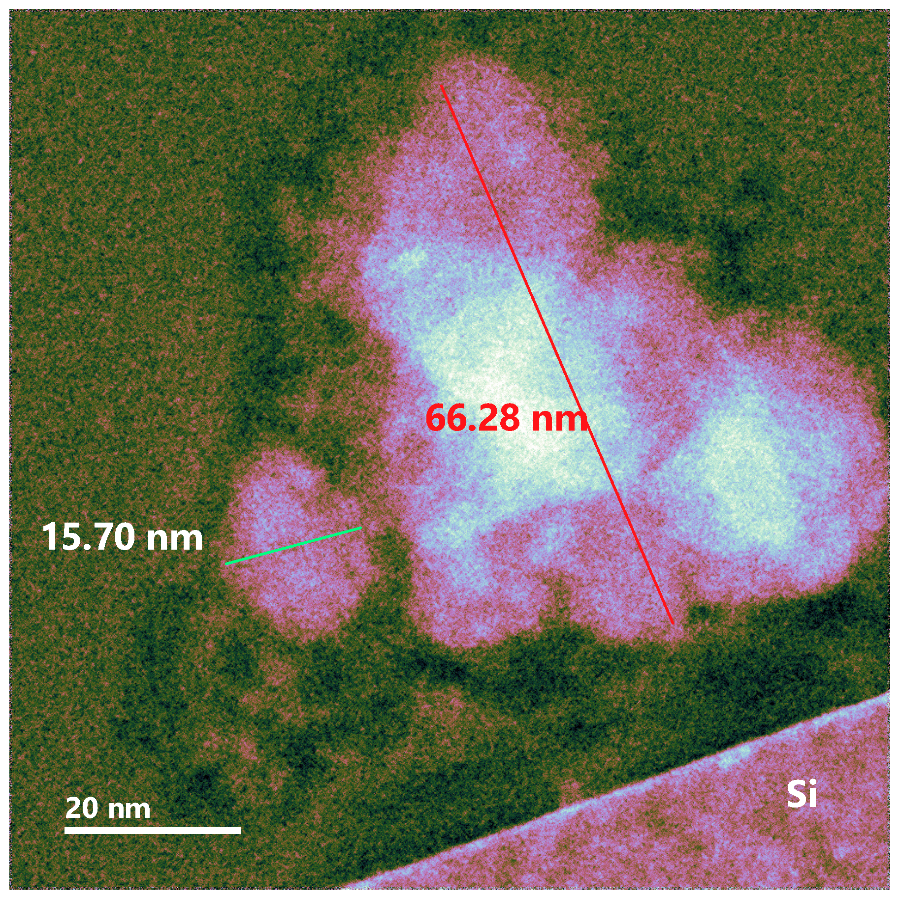
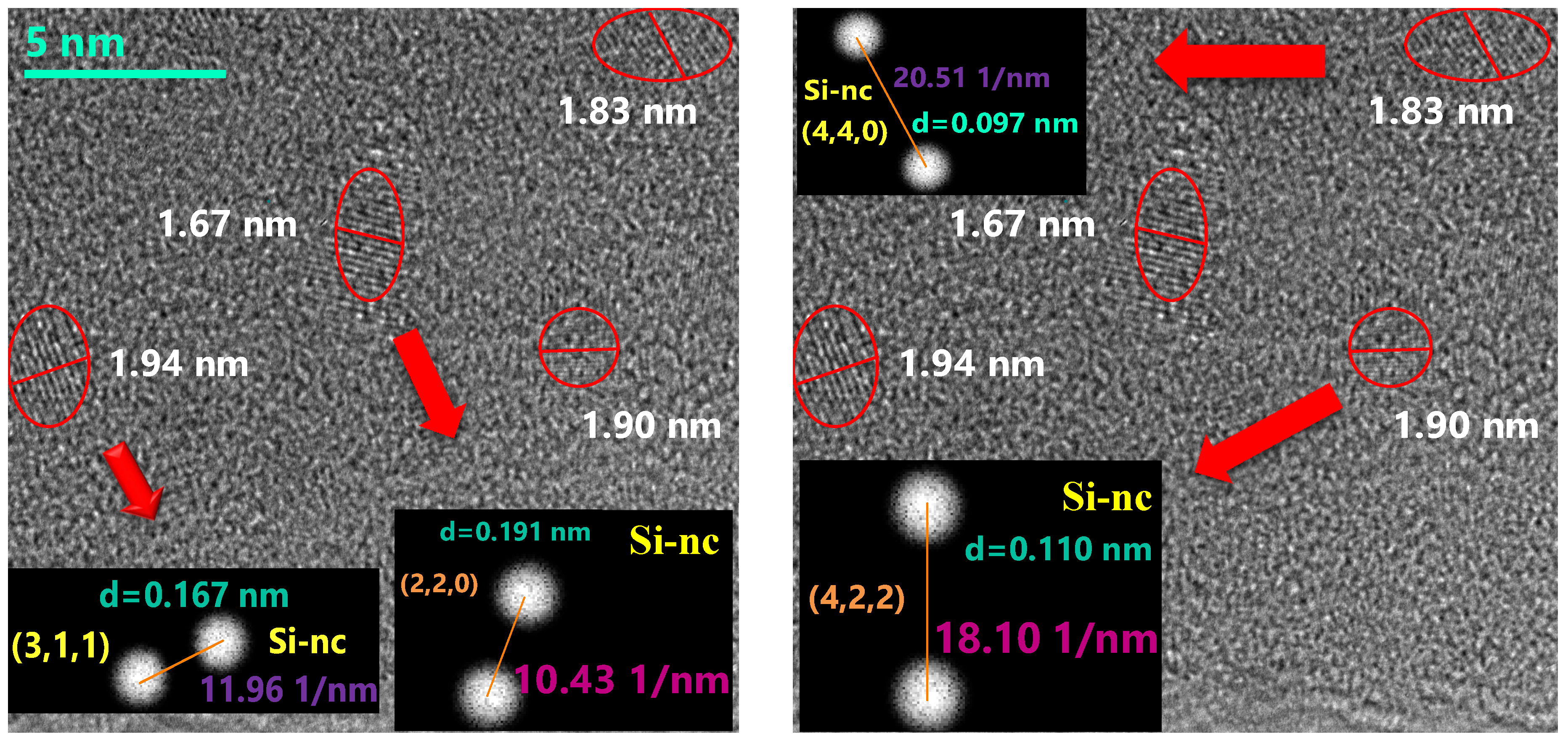
44]; therefore, to complement this study, the HRTEM technique was carried out in order to corroborate the presence of Si-ncs or Si-ncls. The HRTEM micrographs for films A1 and A2 are shown in
Figure 13 and
Figure 14, respectively. These figures show the presence of silicon clusters. In
Figure 13, film A1 has silicon clusters of different sizes and has the largest clusters, which corresponds to what was observed using XPS regarding the presence of Si
0 states; in addition, this film has a greater excess of silicon. In the case of
Figure 14, which shows the micrograph of film A2, the presence of silicon clusters can be seen in the same way, but in this case with a smaller size.
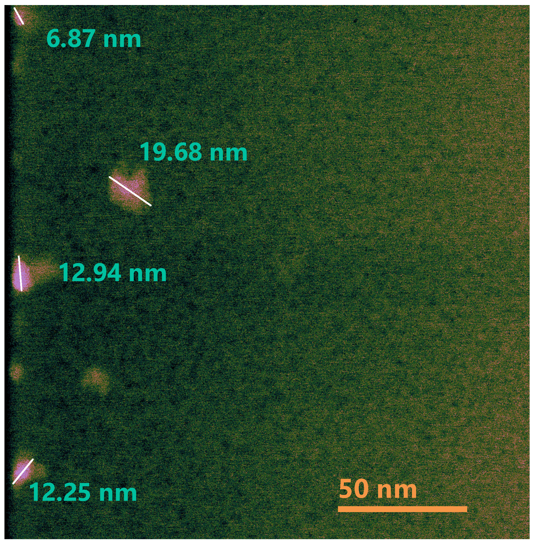
The HRTEM micrographs for films D1 and D2 are shown in
Figure 15 and
Figure 16, respectively. These figures show the presence of dark spots that could represent silicon clusters in which the crystalline orientation was not observed (Si-ncls). They have an average size of 3 nm, which corroborates what was inferred using XPS with respect to the existence of a greater silicon concentration (Si
0 state) in films without thermal annealing.
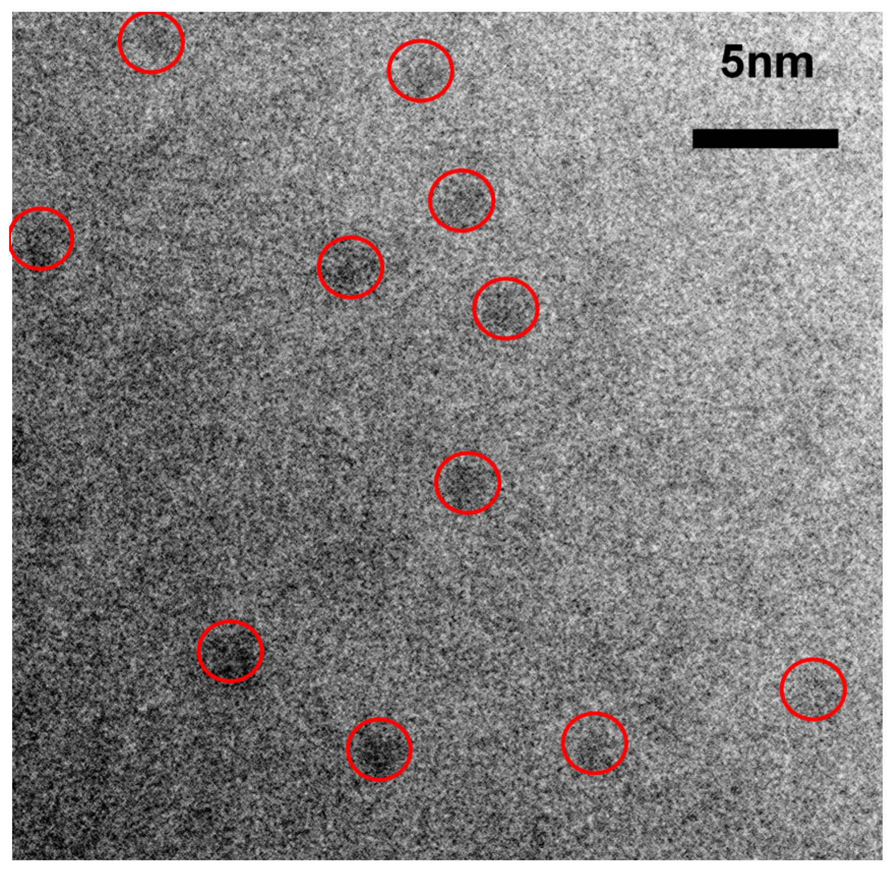
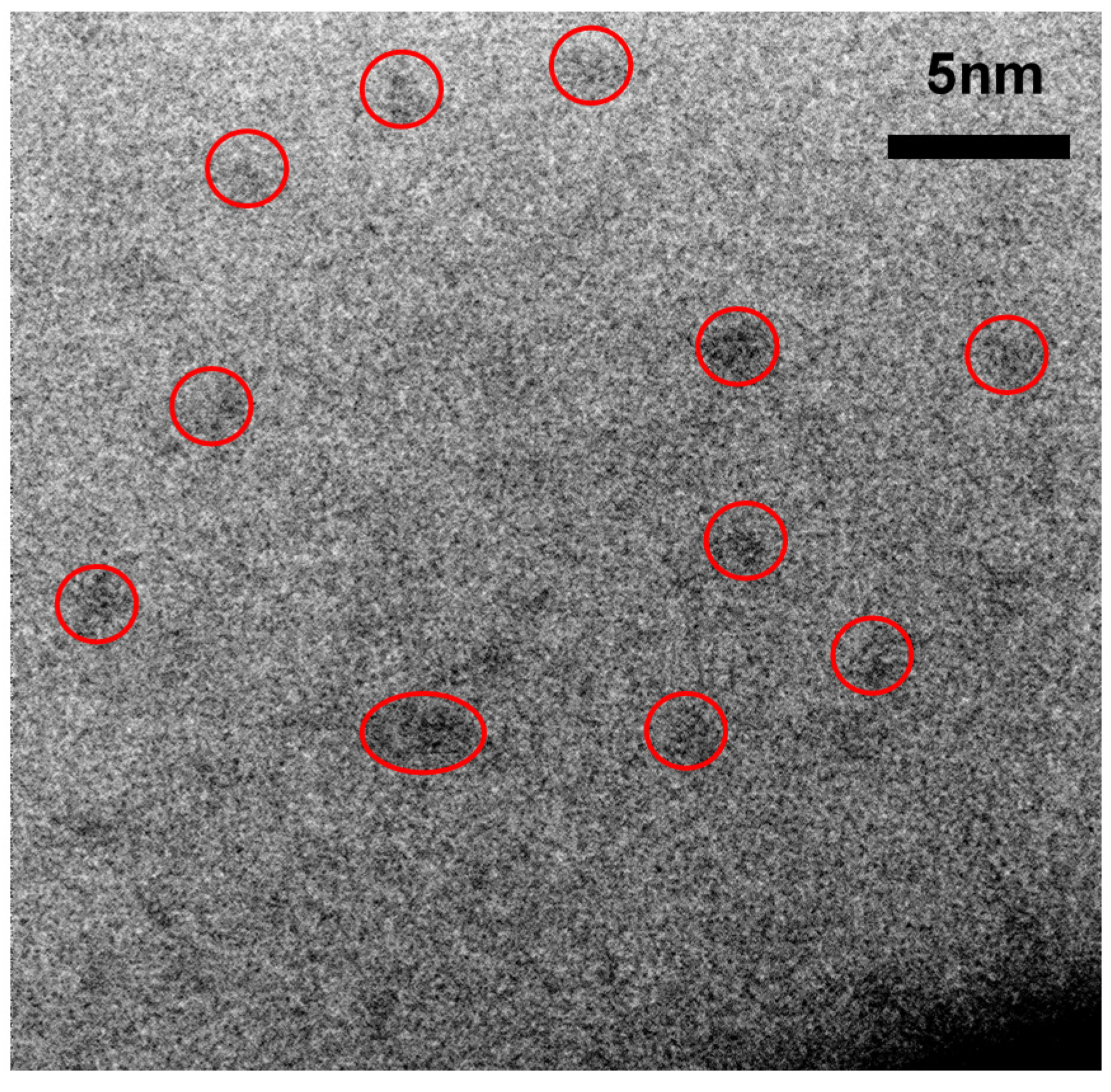
Figure 17 and
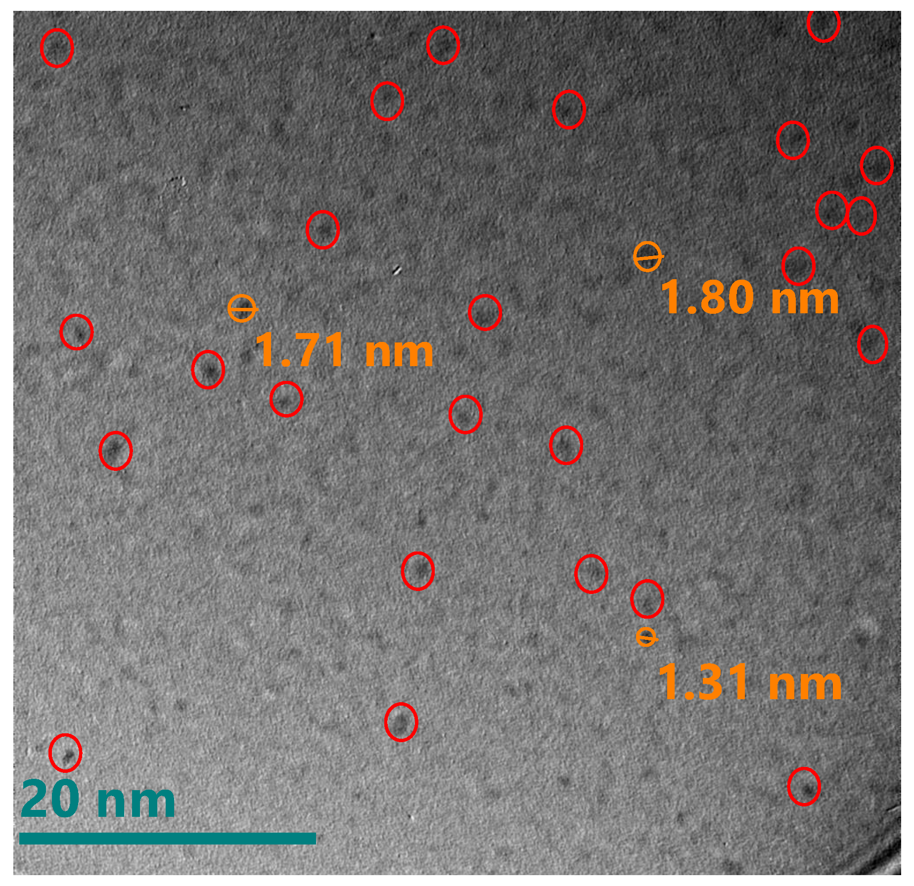
Figure 18 show the HRTEM micrographs of the D1’ fil.,
Figure 17 shows a large number of clusters with a diameter <2 nm, while
Figure 18 shows an enlarged micrograph showing certain regions with dimensions between 1 nm and 2 nm that show a certain crystalline orientation. To obtain the crystallographic orientation, the interplanar distances were measured. The micrographs shown in
Figure 18 were analyzed using a Digital Micrograph program using Fourier transform to obtain the reciprocal space and thus be able to obtain the interplanar distances. With the interplanar distances, we proceeded to search the orientation of the nanocrystals by means of the crystallographic data provided by the database PDF 4. The presence of crystalline silicon with reference code 00-027-1402 is appreciated.
Correlating the results obtained from the various characterizations performed and the micrographs shown, it is important to highlight that the presence of the Si
0 state in all the films without thermal annealing is due to the formation of Si-ncls with sizes greater than 10 nm. In the case of the film A1 which is the one with the highest excess of silicon corresponding to the one that reached the highest temperature of the deposit and has the lowest flow, it also presents Si-ncls of greater size as shown in
Figure 13. The existence of the state Si
0 in the SiO
x films, as can be seen in the phase decomposition, generally occurs after samples are subjected to a thermal annealing above 1000 °C [
31]. This thermal process provokes the formation of Si-ncs in a SiO
2 matrix. With this process the material reaches a stable configuration; however, in this case, when applying thermal annealing, the state Si
0 disappears. This may be due to the resolution reached from the XPS measurement in depth, which may be less than what is required to detect Si-ncs of sizes less than 10 nm.
As previously mentioned, the band of PL emission in the range from 1.3 eV to 1.7 eV is attributed by several authors to the effect of quantum confinement in Si-ncs or silicon Si-ncls [
34,
35,
36]; however, in this theory, the size of the nanocrystal determines the color of the emission. In larger nanocrystals, the emission tends to lower energies, and as we can see from the results, the Si-ncs and Si-ncls are of a size that would correspond to a blue emission. These results make us take into account what is reported by other authors [
35,
45] who suggest that the intense emission around 1.5 eV is caused by small, oxidized silicon grains (1 nm or 2 nm). According to a model of molecular type emitters at the Si/SiO
2 interface in the work of Guerra and Ossicini [
45], the importance of oxidation in nanocrystals for emission is shown, and it is corroborated that those mostly oxidized have a high photoluminescence. This could be compared with that obtained for porous silicon oxidized by Wolking et al. [
46]. In their report it is corroborated that for clusters greater than 3 nm the behavior attributed to quantum confinement (QC) is fulfilled and that when the cluster size is smaller the emission intensity results are greater. In this, case the emission process is attributed to the recombination of the free excitons. For clusters between 2 and 3 nm, the previous behavior is still satisfied but not to the same rate in which it is fulfilled in QC. Here, the recombination is related to a free hole and a trapped electron, and finally, for clusters less than 2 nm, an emission redshift occurs and the recombination processes are attributed to trapped excitons.
Given the size observed in
Figure 17 and
Figure 18, it could be suggested that the thermal annealing in the films induces a phase separation that further reduces the size of the Si-ncl. In addition, by virtue of the presence of interstitial oxygen in the films without annealing, it is possible that an oxidation process occurs of these small, silicon nanocrystals in the Si-nc/SiO
2 interface. Such an event may explain why the PL emission shifts towards red. In addition to the other experimental results obtained regarding the increase in the amount of oxygen in the films and the rearrangement of the molecular network, this would corroborate the theory presented in the literature [
35,
45].

 ,
, 


