Understanding the Role of Temperature and Drain Current Stress in InSnZnO TFTs with Various Active Layer Thicknesses


Abstract

1. Introduction
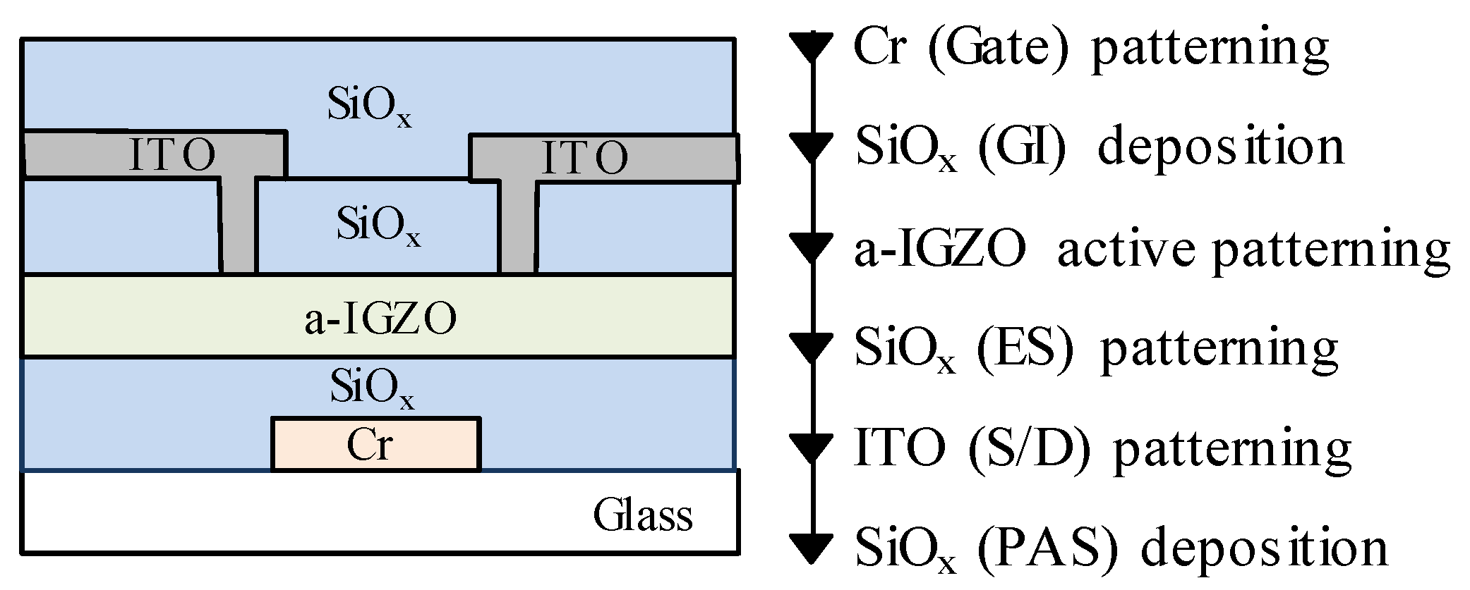
2. Experimental
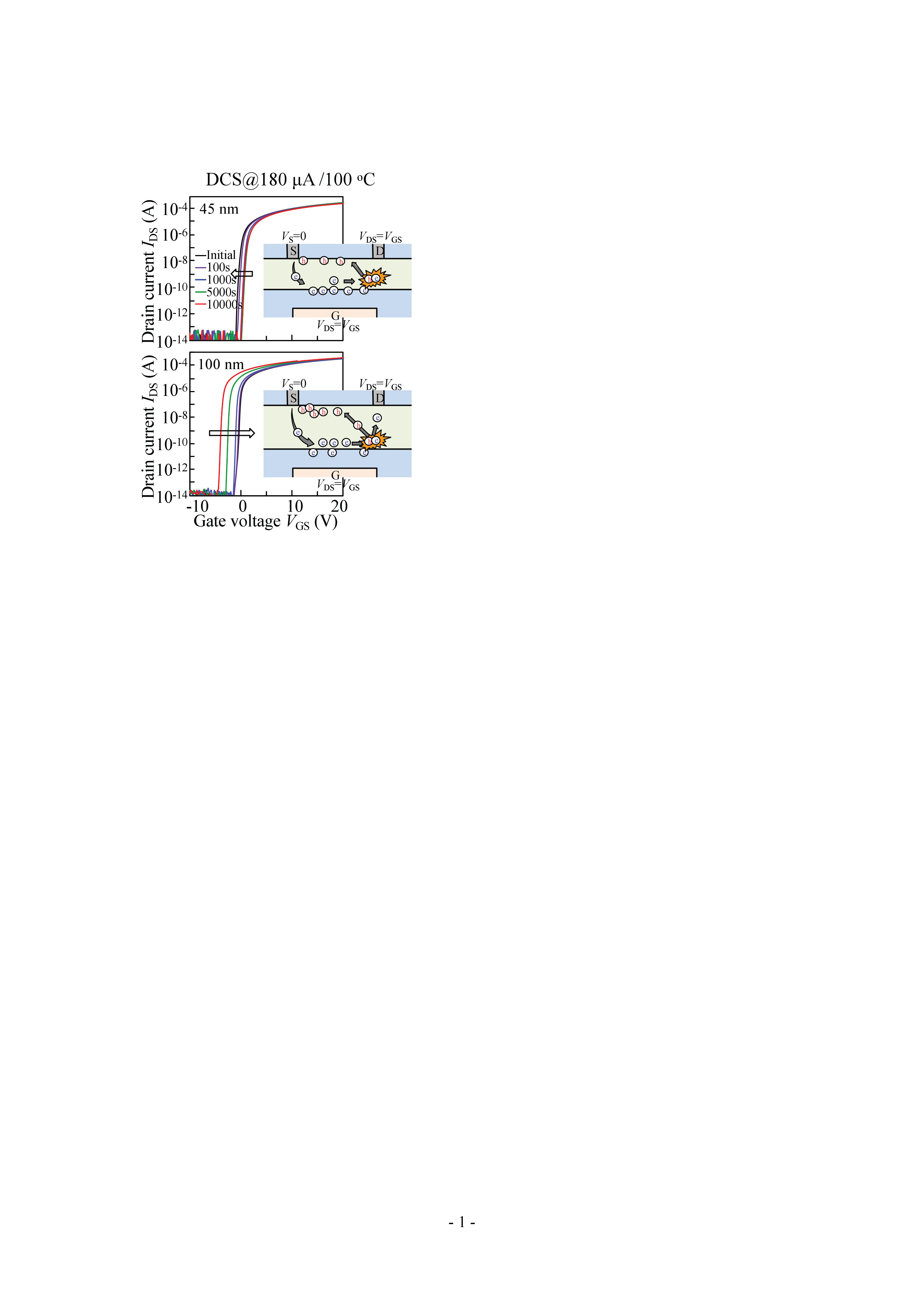
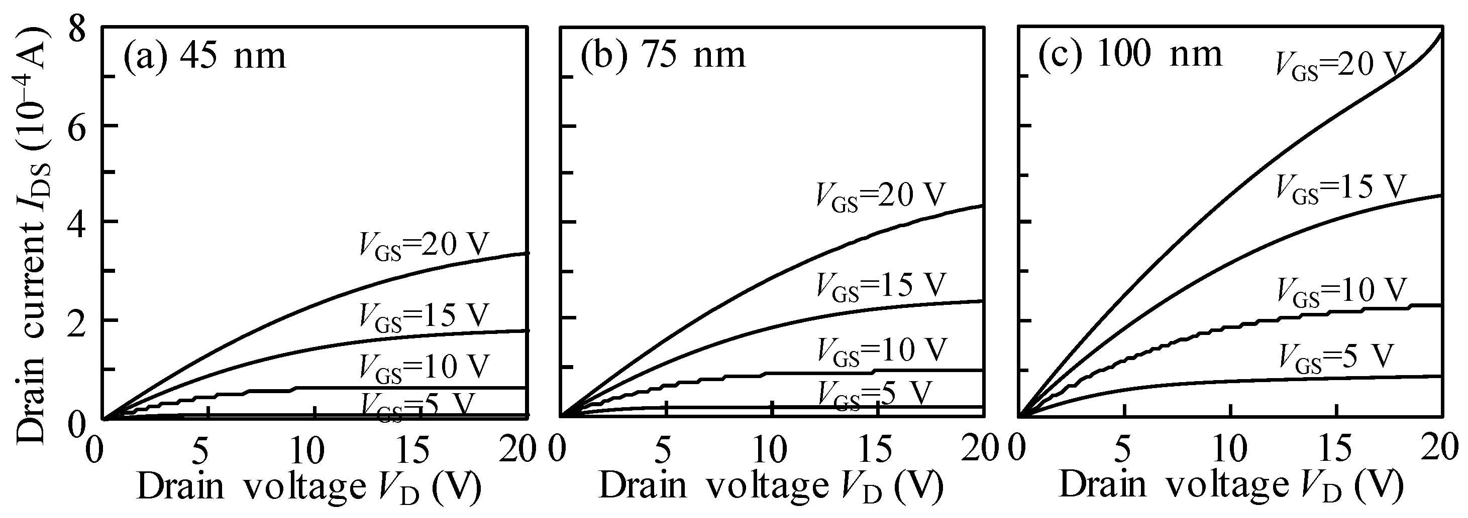
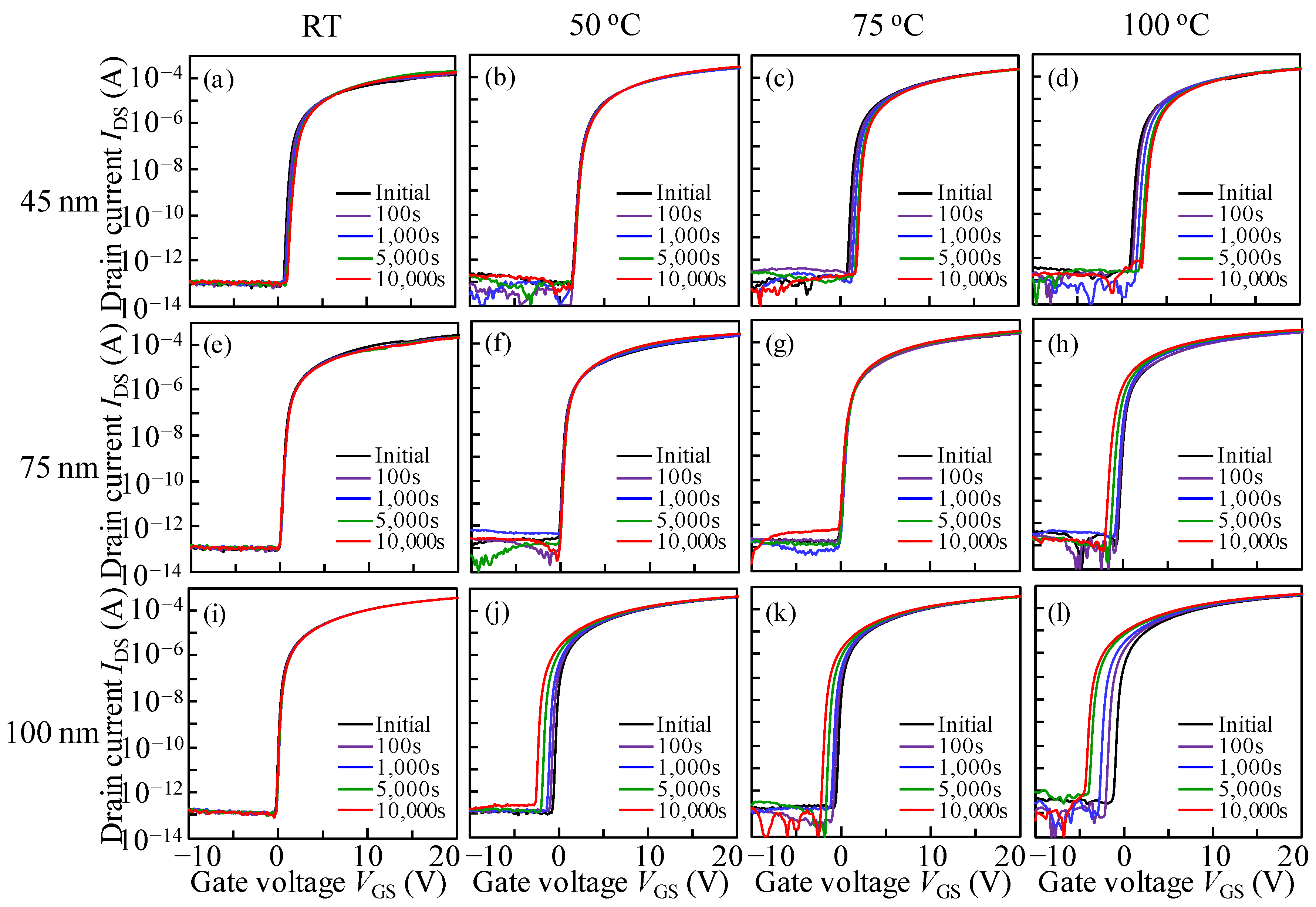
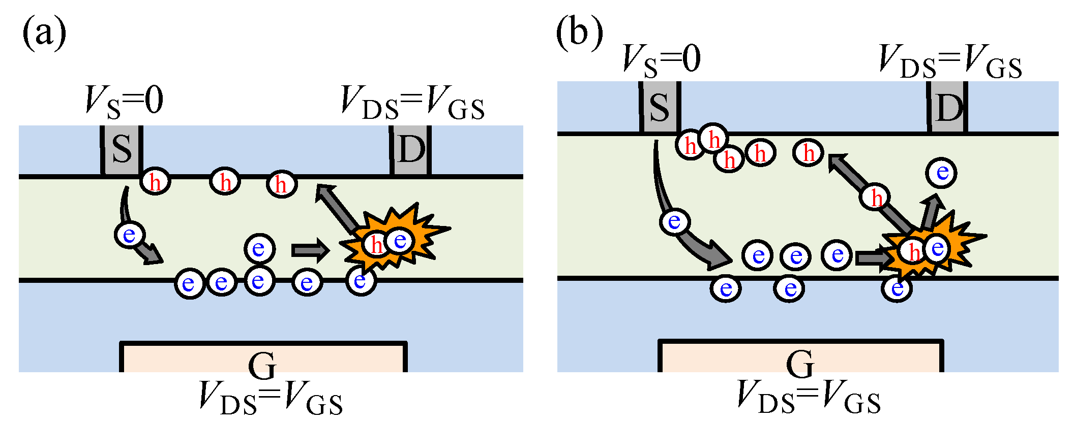
3. Results and Discussion
4. Conclusions
Author Contributions
Funding
Acknowledgments
Conflicts of Interest
References
- Nomura, K.; Ohta, H.; Takagi, A.; Kamiya, T.; Hirano, M.; Hosono, H. Room-temperature fabrication of transparent flexible thin-film transistors using amorphous oxide semiconductors. Nature 2004, 432, 488–492. [Google Scholar] [CrossRef] [PubMed]
- Hirao, T.; Furuta, M.; Hiramatsu, T.; Matsuda, T.; Li, C.; Furuta, H.; Hokari, H.; Yoshida, M.; Ishii, H.; Kakegawa, M. Bottom-gate zinc oxide thin-film transistors (ZnO TFTs) for AM-LCDs. IEEE Trans. Electron Devices 2008, 55, 3136–3142. [Google Scholar] [CrossRef]
- Shin, K.Y.; Tak, Y.J.; Kim, W.-G.; Hong, S.; Kim, H.J. Improvement of Electrical Characteristics and Stability of Amorphous Indium Gallium Zinc Oxide Thin Film Transistors Using Nitrocellulose Passivation Layer. ACS Appl. Mater. Interfaces 2019, 9, 13278–13285. [Google Scholar] [CrossRef] [PubMed]
- Lee, Y.L.; Lee, C.H.; Nam, T.; Lee, S.; Oh, I.-K.; Yang, J.Y.; Choi, D.W.; Yoo, C.; Kim, H.-J.; Kim, W.-H.; et al. Hydrogen barrier performance of sputtered La2O3 films for InGaZnO thin-film transistor. J. Mater. Sci. 2019, 54, 11145–11156. [Google Scholar] [CrossRef]
- Wang, C.-J.; You, H.-C.; Ou, J.-H.; Chu, Y.-Y.; Ko, F.-H. Ultraviolet Photodetecting and Plasmon-to-Electric Conversion of Controlled Inkjet-Printing Thin-Film Transistors. Nanomaterials 2020, 10, 458. [Google Scholar] [CrossRef]
- Barros, R.; Saji, K.J.; Waerenborgh, J.C.; Barquinha, P.; Pereira, L.; Carlos, E.; Martins, R.; Fortunato, E. Role of Structure and Composition on the Performances of P-Type Tin Oxide Thin-Film Transistors Processed at Low-Temperatures. Nanomaterials 2019, 9, 320. [Google Scholar] [CrossRef]
- Zan, H.-W.; Yeh, C.-C.; Meng, H.-F.; Tsai, C.-C.; Chen, L.H. Achieving High Field-Effect Mobility in Amorphous Indium-Gallium-Zinc Oxide by Capping a Strong Reduction Layer. Adv. Mater. 2012, 24, 3509–3514. [Google Scholar] [CrossRef]
- Wang, C.-J.; You, H.-C.; Lin, K.; Ou, J.-H.; Chao, K.-H.; Ko, F.-H. Highly Transparent and Surface-Plasmon-Enhanced Visible-Photodetector Based on Zinc Oxide Thin-Film Transistors with Heterojunction Structure. Materials 2019, 12, 3639. [Google Scholar] [CrossRef]
- Zhou, C.; Ai, Q.; Chen, X.; Gao, X.; Liu, K.; Shen, D. Ultraviolet photodetectors based on wide bandgap oxide semiconductor films. Chin. Phys. B 2019, 28, 048503. [Google Scholar] [CrossRef]
- Zhao, W.; Li, H.; Li, D.; Liu, Z.; Wang, D.; Liu, S. Comprehensive investigation of sputtered and spin-coated zinc oxide electron transport layers for highly efficient and stable planar perovskite solar cells. J. Power Sources 2019, 427, 223–230. [Google Scholar] [CrossRef]
- Li, H.; Li, D.; Zhao, W.; Yuan, S.; Liu, Z.; Wang, D.; Liu, S. NaCl-Assisted Defect Passivation in the Bulk and Surface of TiO2 Enhancing Efficiency and Stability of Planar Perovskite Solar Cells. J. Power Sources 2020, 448, 227586. [Google Scholar] [CrossRef]
- Wang, D.; Li, C.; Furuta, M. Influence of Active Layer Thickness on Performance and Reliability of InSnZnO Thin-film Transistors. In Proceedings of the 19th International Workshop on AM-FPD, Kyoto, Japan, 4–6 July 2012; pp. 159–162. [Google Scholar]
- Nakata, M.; Zhao, C.; Kanicki, J. DC sputtered amorphous In–Sn–Zn–O thin-film transistors: Electrical properties and stability. Solid State Electron. 2016, 116, 22–29. [Google Scholar] [CrossRef]
- Park, H.-W.; Park, K.; Kwon, J.-Y.; Choi, D.; Chung, K.-B. Effect of active layer thickness on device performance of tungsten-doped InZnO thin-film transistor. IEEE Trans. Electron Devices 2016, 64, 159–163. [Google Scholar] [CrossRef]
- Park, J.; Kim, Y.S.; Kim, J.H.; Park, K.; Park, Y.C.; Kim, H.-S. The effects of active layer thickness and annealing conditions on the electrical performance of ZnON thin-film transistors. J. Alloy. Compd. 2016, 688, 666–671. [Google Scholar] [CrossRef]
- Yang, Z.; Yang, J.; Meng, T.; Qu, M.; Zhang, Q. Influence of channel layer thickness on the stability of amorphous indium zinc oxide thin film transistors. Mater. Lett. 2016, 166, 46–50. [Google Scholar] [CrossRef]
- Wang, D.; Hung, M.P.; Jiang, J.; Toda, T.; Furuta, M. Suppression of degradation induced by negative gate bias and illumination stress in amorphous InGaZnO thin-film transistors by applying negative drain bias. ACS Appl. Mater. Interfaces 2014, 6, 5713–5718. [Google Scholar] [CrossRef]
- Zhang, J.; Yang, J.; Li, Y.; Wilson, J.; Ma, X.; Xin, Q.; Song, A. High performance complementary circuits based on p-SnO and n-IGZO thin-film transistors. Materials 2017, 10, 319. [Google Scholar] [CrossRef]
- Lee, S.; Chen, Y.; Kim, J.; Kim, H.-M.; Jang, J. Transparent AMOLED display driven by split oxide TFT backplane. J. Soc. Inf. Disp. 2018, 26, 164–168. [Google Scholar] [CrossRef]
- Chen, Y.; Geng, D.; Jang, J. Integrated Active-Matrix Capacitive Sensor Using a-IGZO TFTs for AMOLED. IEEE J. Electron Devices Soc. 2018, 6, 214–218. [Google Scholar] [CrossRef]
- Wang, D.; Zhao, W.; Li, H.; Furuta, M. Drain Current Stress-Induced Instability in Amorphous InGaZnO Thin-Film Transistors with Different Active Layer Thicknesses. Materials 2018, 11, 559. [Google Scholar] [CrossRef]
- Yue, L.; Pu, H.-F.; Li, H.-L.; Pang, S.-J.; Zhang, Q. Effect of active layer thickness on device performance of a-LZTO thin-film transistors. Superlattice Microstruct. 2013, 57, 123–128. [Google Scholar] [CrossRef]
- Lee, S.; Jeon, S.; Nathan, A. Modeling Sub-Threshold Current–Voltage Characteristics in Thin Film Transistors. J. Disp. Technol. 2013, 9, 883–889. [Google Scholar]
- Kamiya, T.; Hosono, H. Material characteristics and applications of transparent amorphous oxide semiconductors. NPG Asia Mater. 2010, 2, 15–22. [Google Scholar] [CrossRef]
- Choi, H.-S.; Jeon, S.; Kim, H.; Shin, J.; Kim, C.; Chung, U.I. The impact of active layer thickness on low-frequency noise characteristics in InZnO thin-film transistors with high mobility. Appl. Phys. Lett. 2012, 100, 173501. [Google Scholar] [CrossRef]
- Valdinoci, M.; Colalongo, L.; Baccarani, G.; Fortunato, G.; Pecora, A.; Policicchio, I. Floating body effects in polysilicon thin-film transistors. IEEE Trans. Electron Devices 1997, 44, 2234–2241. [Google Scholar] [CrossRef]
- Jiang, J.; Wang, D.; Matsuda, T.; Kimura, M.; Liu, S.; Furuta, M. Influence of Interface Traps on the Electrical Properties of Oxide Thin-Film Transistors with Different Channel Thicknesses. J. Nano Res. 2017, 46, 93–99. [Google Scholar] [CrossRef]
- Li, Y.; Pei, Y.L.; Hu, R.Q.; Chen, Z.M.; Zhao, Y.; Shen, Z.; Fan, B.F.; Liang, J.; Wang, G. Effect of channel thickness on electrical performance of amorphous IGZO thin-film transistor with atomic layer deposited alumina oxide dielectric. Curr. Appl. Phys. 2014, 14, 941–945. [Google Scholar] [CrossRef]
- Lee, H.; Lin, Y.-C.; Shieh, H.P.D.; Kanicki, J. Current-scaling a-Si:H TFT pixel-electrode circuit for AM-OLEDs: Electrical properties and stability. IEEE Trans. Electron Devices 2007, 54, 2403–2410. [Google Scholar]


| Thickness (nm) | 45 | 75 | 100 |
|---|---|---|---|
| μlin (cm2∙V−1∙s−1) | 28.76 | 33.27 | 46.36 |
| μsat (cm2∙V−1∙s−1) | 35.23 | 46.90 | 130.10 |
| VON at IDS = 1 nA (V) | 1.19 | 0.43 | −0.33 |
| Hysteresis ΔVH (V) | 0.22 | 0.07 | −6.38 |
| Subthreshold swing (mV/dec.) | 169 | 130 | 88 |
© 2020 by the authors. Licensee MDPI, Basel, Switzerland. This article is an open access article distributed under the terms and conditions of the Creative Commons Attribution (CC BY) license (http://creativecommons.org/licenses/by/4.0/).
Share and Cite
Wang, D.; Furuta, M.; Tomai, S.; Yano, K. Understanding the Role of Temperature and Drain Current Stress in InSnZnO TFTs with Various Active Layer Thicknesses. Nanomaterials 2020, 10, 617. https://doi.org/10.3390/nano10040617
Wang D, Furuta M, Tomai S, Yano K. Understanding the Role of Temperature and Drain Current Stress in InSnZnO TFTs with Various Active Layer Thicknesses. Nanomaterials. 2020; 10(4):617. https://doi.org/10.3390/nano10040617
Chicago/Turabian StyleWang, Dapeng, Mamoru Furuta, Shigekazu Tomai, and Koki Yano. 2020. "Understanding the Role of Temperature and Drain Current Stress in InSnZnO TFTs with Various Active Layer Thicknesses" Nanomaterials 10, no. 4: 617. https://doi.org/10.3390/nano10040617
APA StyleWang, D., Furuta, M., Tomai, S., & Yano, K. (2020). Understanding the Role of Temperature and Drain Current Stress in InSnZnO TFTs with Various Active Layer Thicknesses. Nanomaterials, 10(4), 617. https://doi.org/10.3390/nano10040617