Article

Border Trap Characterizations of Al2O3/ZrO2 and Al2O3/HfO2 Bilayer Films Based on Ambient Post Metal Annealing and Constant Voltage Stress

1
School of Science and Engineering, Department of EEE, Canadian University of Bangladesh, Dhaka 1213, Bangladesh
2
School of Electrical Engineering, University of Ulsan, Ulsan 44610, Korea
3
School of Electronics Engineering, Kyungpook National University, Daegu 702-701, Korea
*
Authors to whom correspondence should be addressed.
Nanomaterials 2020, 10(3), 527; https://doi.org/10.3390/nano10030527
Submission received: 3 February 2020 / Revised: 1 March 2020 / Accepted: 12 March 2020 / Published: 15 March 2020

Abstract

:
This study represents a comparison of the border trap behavior and reliability between HfO2 and ZrO2 films on n-In0.53Ga0.47As with an Al2O3 interfacial layer. The effect of different post metal annealing conditions on the trap response was analyzed and it was found that the N2:H2 mixed FGA passivates the border trap quite well, whereas N2-based RTA performs better on interface traps. Al2O3/HfO2 showed more degradation in terms of the threshold voltage shift while Al2O3/ZrO2 showed higher leakage current behavior. Moreover, Al2O3/ZrO2 showed a higher permittivity, hysteresis, and breakdown field than Al2O3/HfO2.

1. Introduction

As potential gate insulator candidates in III–V channel material-based nano-metric metal oxide semiconductor field-effect transistors (MOSFETs), which are considered as a future device for logic applications with a higher speed and bottled-up power consumption, the most studied Hf and Zr-based high-k oxides suffer from a lower barrier elevation as well as a destitute interface with the semiconductor material compared to the SiO2/Si-based system. These shortcomings are hindrances to achieving the leakage current challenge [1,2,3,4,5]. To solve these issues, an interfacial layer of Al2O3 is added between the above-mentioned dielectric materials and semiconductor. This forms a bilayer arrangement of a gate oxide structure since Al2O3 possesses the supremacy of a higher bandgap with a significant barrier offset and an improved surface passivation scheme with the channel material [5,6,7].
Among the III–V family, which is considered as a next-generation channel material instead of Si as it is in the material limit, indium-rich InxGa1-xAs materials with x = 0.53 have received a lot of attention due to their nearly eight times higher electron mobility compared to Si and their higher injection velocity. In addition, these materials have already been developed in defense and high-frequency analog applications [8,9]. The high velocities are attained by reimbursing a lower effective mass which causes the “density of state bottleneck” dilemma which pins the fermi level, EF, inside the conduction band, resulting in a reduction of the conduction band distinction height [9,10,11]. This disposition of the fermi level makes itself align with the border trap’s energy levels, which are located near the interfacial oxide region with the semiconductor inside the oxide [10,12]. When an AC signal is superimposed with the applied DC bias, there is a tunneling of channel electrons into or emitting between the border traps and the semiconductor. Usually, these near interfacial traps are categorized by their position inside the oxide; the furthermost trap takes the longest time to fill. So this charge exchange time is characterized by the depth of the traps inside the oxide which also depends on the applied frequency [10,13]. This creates a frequency dependent capacitance response in the accumulation and these traps are also responsible for dilapidation of mobility, on-state current, transconductance, and reliability by causing high hysteresis, threshold voltage instability, and phonon scattering [10,11,12,14]. Moreover, as a reliability issue, it has already been reported that the constant-voltage-stress (CVS) is responsible for electron trapping in these acceptors like oxide traps as well as the creation of new oxygen vacancy defects [8,15,16].
The conventional interface trap model is unable to explain the border trap behavior due to a time constant mismatch between both types of traps, as well as the border trap estimation from capacitance-voltage (C–V) hysteresis, which suffers from complete re-emission of captured charge at the C–V reverse sweep. Consequently, it is appropriate to characterize these traps by regarding accumulation frequency dispersion [3,17]. Furthermore, there are already several reports regarding border trap reduction by following some annealing process, although a clear understanding of the annealing ambient is lacking [16,17,18]. In addition, although both HfO2 and ZrO2 are considered to have almost the same electrical and chemical properties and there are reports of their physical, chemical, and electrical characterizations, there is still an opportunity to investigate the oxide trap characterization between these oxides [6,16]. In this study, we characterized the trap responses between HfO2 and ZrO2 oxides along with an Al2O3 interfacial layer in a bilayer form with different annealing environments as well as under different stress voltage conditions in the CVS environment.

2. Materials and Methods

The Al2O3, HfO2, and ZrO2 films were deposited on n-In0.53Ga0.47As by atomic layer deposition (ALD) using trimethylaluminum (TMA), tetrakis (ethymethylamino) hafnium (TEMAH), and ZrCl4 as the metal precursors for Al2O3, HfO2, and ZrO2, respectively, where H2O was the oxidant and N2 was used as both the carrier and purge gas. The details of the epitaxial growth of n-In0.53Ga0.47As on a 300 mm thick n-Si (001) substrate were described in our previous report [19]. Before deposition, the substrate was cleaned by a standard wet cleaning process, which incorporated hydrochloric acid (HCl) and deionized (DI) water to remove the contaminants and native oxide from the surface. Then, the substrate was dried in a nitrogen(N2) environment for the prevention of water mask formation on the surface and transferred to the ALD chamber (“Atomic Classic”, CN1, Gyenggi-do, Korea) within a minimal time interval. Before the actual film deposition, the substrates were pretreated with 10 cycles of TMA pulses to passivate the surface due to its’ “self-cleaning effect” [10]. Then, two individual depositions of Al2O3/ZrO2 (1 nm/3.3 nm) and Al2O3/HfO2 (1 nm/3 nm) were performed followed by ALD TiN (5 nm) deposition on the top of the oxide layer. Then, for the front side metal electrode, a layer of Ti/Au (200/2000 Å) was deposited by e-beam evaporation (Temescal, Zeus Co, Ltd.; Yongin, Korea, model: FC-2000) via lift-off and the same metal layer was also deposited for the backside contact. To isolate the metal-oxide-semiconductor capacitors (MOSCAPS), reactive ion etching (RIE) was performed based on SF6/Ar gas (30/10 sccm) to remove the TiN layer. Then, the devices were separately processed by post-metal annealing (PMA) at 350 °C in a N2, H2, and O2 environment for 1 min to observe the passivation effect on the electrically active defects in the high-k/In0.53Ga0.47As interface and oxide itself. Another set of devices were annealed in forming gas (N2:H2 = 96%:4%) for 30 min at 300 °C. The electrical characterizations were carried out in the dark environment using a Keithley 4200A-SCS parameter analyzer (Tektronix, Inc., Beaverton, OR, USA) at room temperature and the CVS measurements were obtained using a Keysight CV-enabled B1500A semiconductor device parameter analyzer.

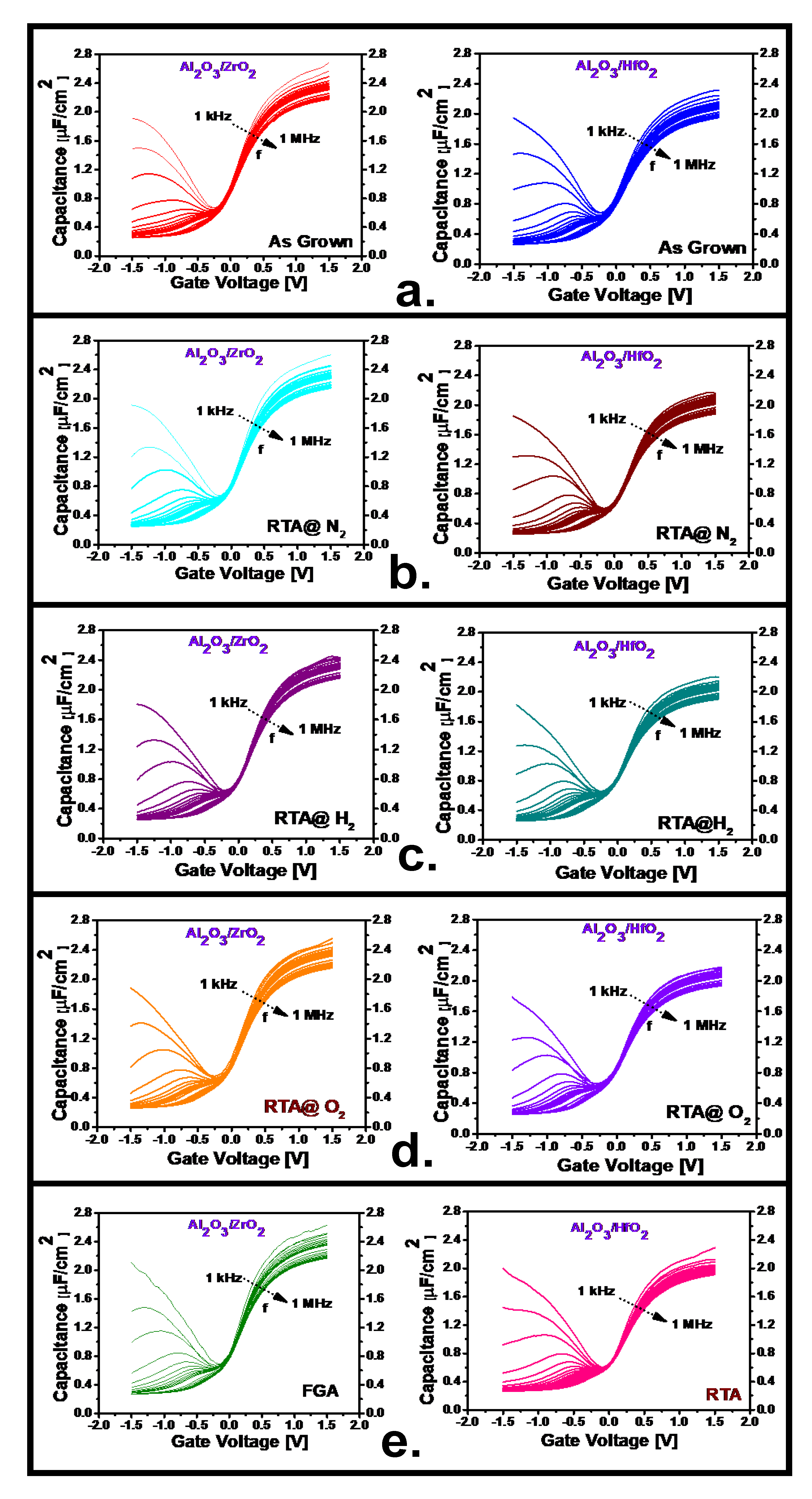
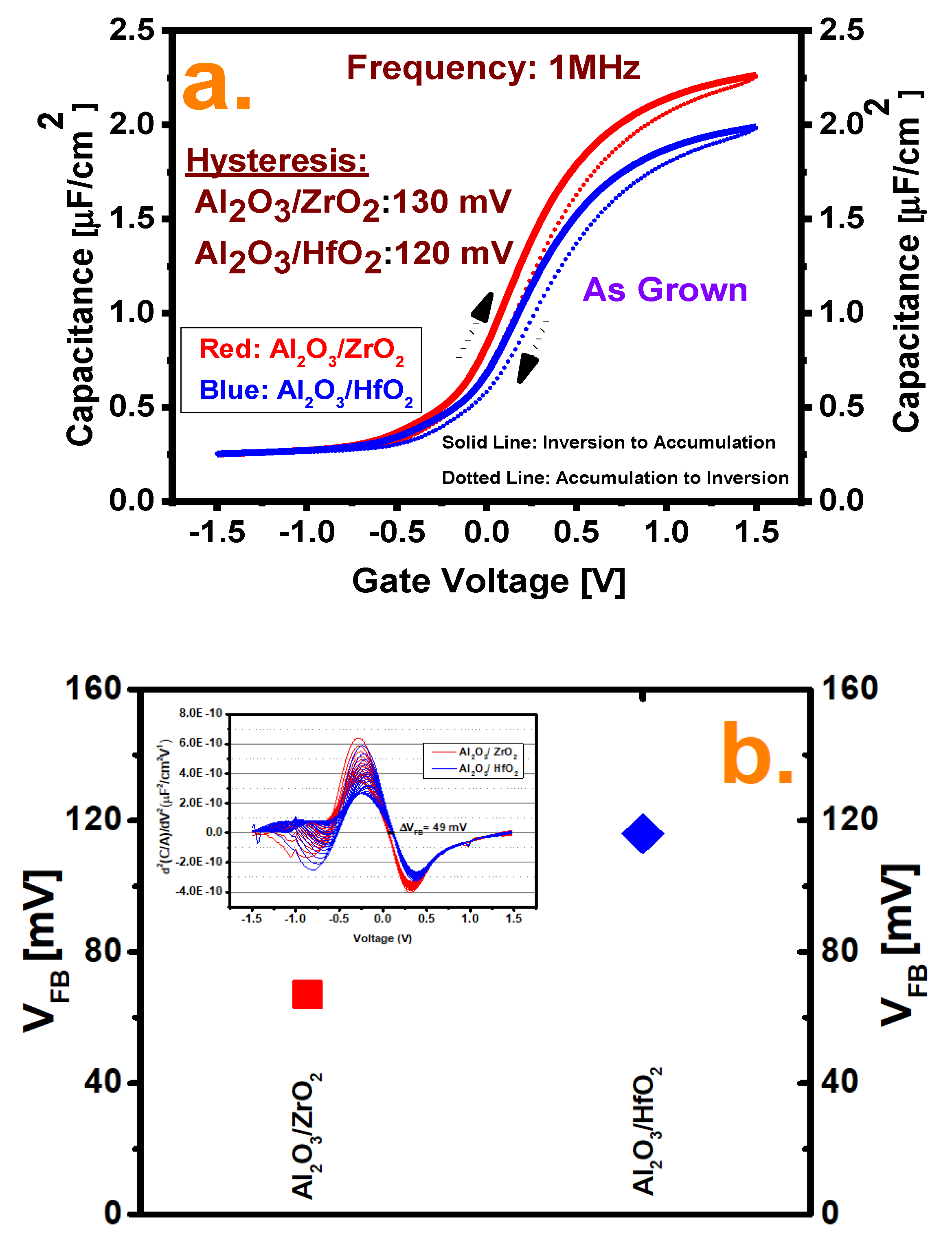
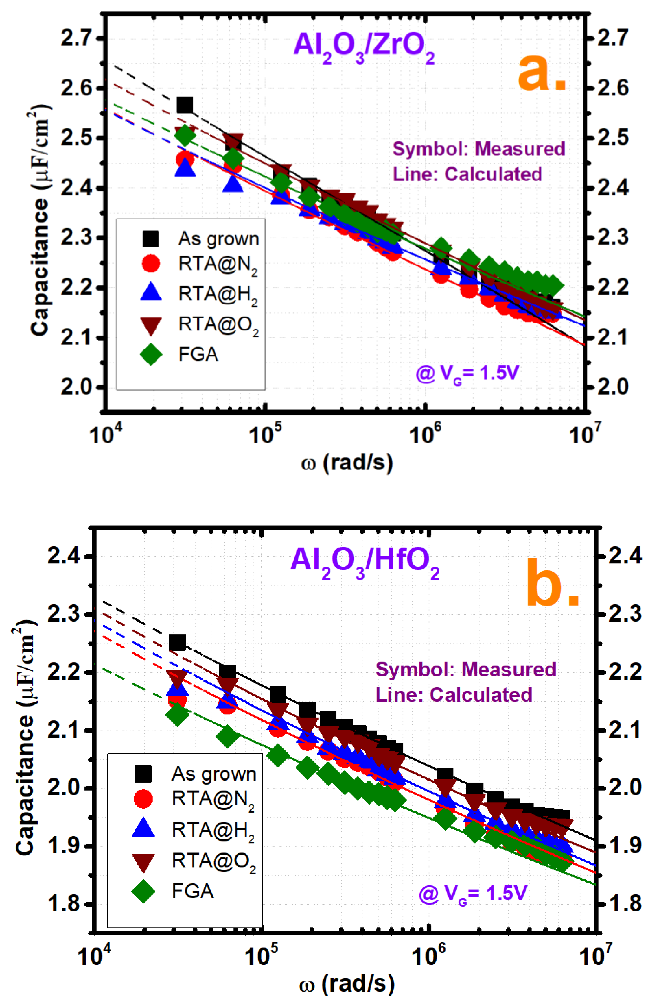
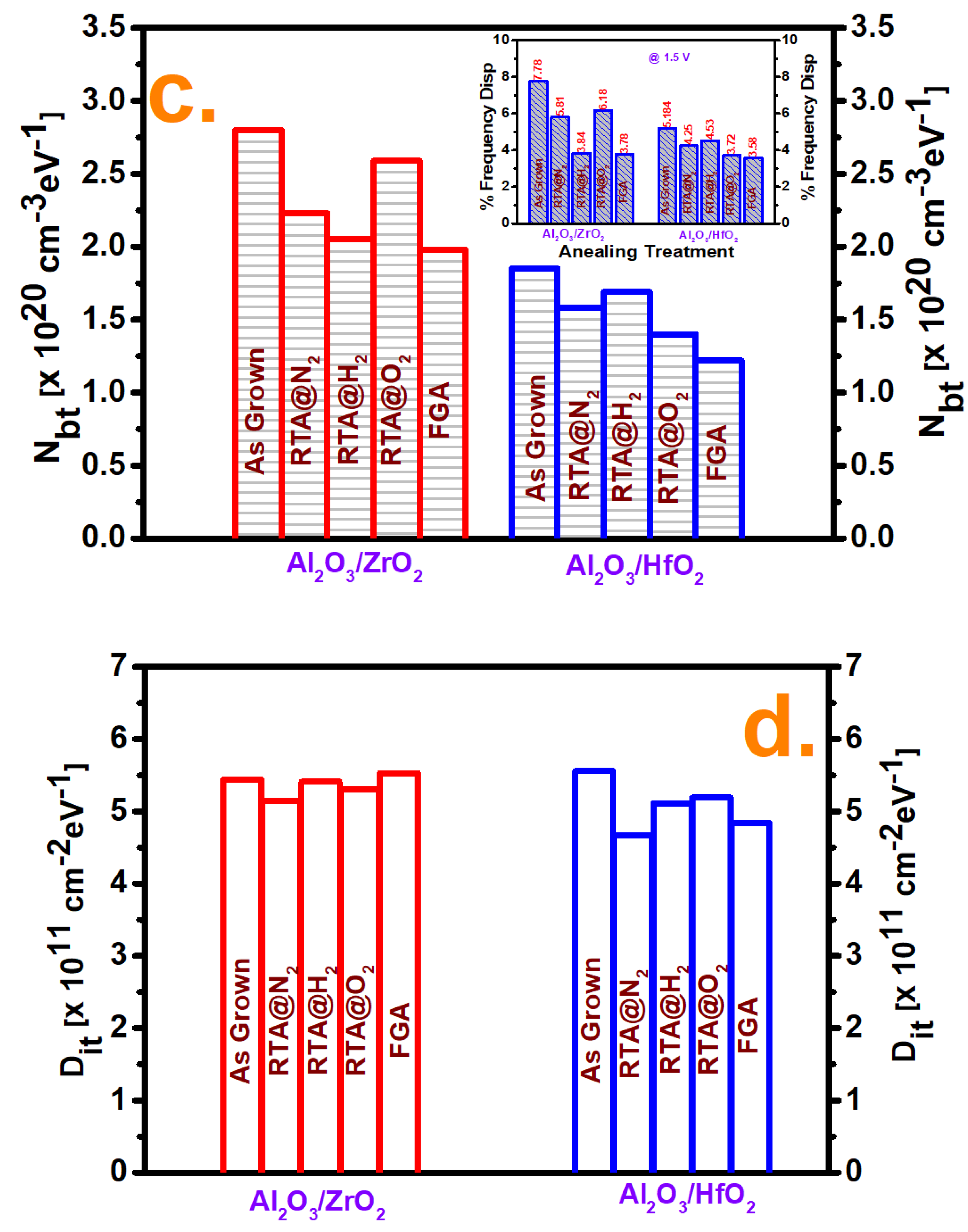
3. Results and Discussion

Figure 1 illustrates the measured capacitive-voltage response of the two samples along with the extracted dielectric constant (keffective) and the calculated capacitive equivalent thickness (CET). In Figure 1a, the measured frequency dependent C–V responses are plotted for 1 kHz–1 MHz with a voltage range of −1.5 V to +1.5 V for both samples under as-grown conditions. Although the inversion responses are the same in both cases, there is more dispersion in the accumulation region of the Al2O3/ZrO2 than in the Al2O3/HfO2, which indicates a higher density of border traps (Nbt) presented in it. Furthermore, the higher accumulation capacitance also indicates greater permittivity of the Al2O3/ZrO2 film. From Figure 1b–e, frequency dispersion is presented of both samples for the cases of PMA treatments at different ambient. From all of these figures, it is evident that the frequency dispersion was reduced compared to the as-grown condition after these treatments although the amount of reduction varied based on the ambient type. This reduction indicates a minimization of border trap density (Nbt) and the highest amount of trap depreciation was obliged for both samples by FGA treatment, which was indicated by the lowest amount of frequency dispersion as observed in Figure 1e. The amount of frequency dispersion along with border trap density (Nbt) reductions are characterized later. Figure 1f demonstrates the extracted keffective value from the measured 1 kHz frequency response of the two deposition cases depending on the different annealing treatments by using the process as described in our previous report [10]. The extracted keffective values at the as-grown condition for the Al2O3/ZrO2 film are 13.07 and 10.44 for Al2O3/HfO2 while the permittivity values for Al2O3/ZrO2 in all PMA treatment cases are higher than those of Al2O3/HfO2, which indicates the higher permittivity of the ZrO2 film compared to HfO2 since Al2O3 has the same thickness in both cases [20]. Furthermore, the permittivity decreased in both samples after all types of PMA treatment compared to the as-grown condition, which indicates interfacial layer formation with a lower permittivity as well as some intermixing effect in between the high-k and InGaAs surface [20]. For the Al2O3/ZrO2 sample, the lowest permittivity value was found for the H2 treated case which was 11.64 and for the Al2O3/HfO2 sample, it was for the O2 treated case which had a value of 9.74. The other treated cases have the values within these limits. The CET values, as depicted in Figure 1g, extracted from the accumulation capacitance from 100 kHz at the maximum bias voltage, as mentioned in a previous report, for both samples have almost identical for both the as-grown and annealed conditions [10]. Although there is a little variation in CET values between different annealed conditions of both samples, from the figure, it can be inferred that the CET values of the as-grown samples had not faced a significant change.
Figure 2a shows the hysteresis comparison of the two samples under as-grown conditions measured at a frequency of 1 MHz to minimize the trap response by starting the C–V sweep at a sweep speed of 20 mV/s from inversion to accumulation and without any holding delay back to inversion. From the figure, it is detected that the Al2O3/ZrO2 sample shows higher hysteresis (130 mV) than Al2O3/HfO2 (120 mV). The higher hysteresis value indicates more charge trapping at the border traps. The charge traps into these vacancies when the fermi level becomes aligned with the trap energy level at the accumulation region and when the C–V sweep reverses back, which cannot be moved away unless the fermi level becomes closer to the valance band and makes a voltage shift. Figure 2b shows the flat-band voltages (VFB) of the two samples extracted by the infection point method by calculating the second derivative of normalized C–V data as illustrated in the inset of Figure 2b, where VFB shows a left shift for Al2O3/ZrO2 compared to Al2O3/HfO2, which can be explained by the elimination of electron traps by the ZrO2 dielectric itself, as well as the incidence of positive charges [20,21].
Figure 3 depicts the trap characterizations as well as the frequency dispersions of both samples under different annealing conditions. The border trap density (Nbt) was characterized by the distributed border trap model proposed by Yaun et al. by making the best fit between the measured capacitance at the specific voltage in the accumulation region and the capacitance calculated from the model [22]. In this model, the total oxide thickness is segmented into a small number of quantities. Every quantity represents a certain amount of oxide capacitance which is in a parallel configuration of admittance that is proportional to border trap quantities and is in a series configuration with semiconductor capacitance. A detailed explanation of this model and extraction process of Nbt was described in our previous report [10]. However, in the extraction process, the effective electron masses of the Al2O3, HfO2, and ZrO2 films were considered as 0.23 m0, 0.22 m0, and 0.3 m0, respectively, where m0 represents the electron rest mass [17,23]. In addition, a one-dimensional Poisson–Schrodinger solver simulation tool (Nextnano) was used to calculate the semiconductor capacitance Cs at border trap extraction voltage [24]. Figure 3a, b shows the fitting curves between the measured and calculated capacitance for both cases. From Figure 3c, it is observed that Nbt is higher in the Al2O3/ZrO2 (2.8 × 1020 cm−3·eV−1) film compared to the Al2O3/HfO2 (1.85 × 1020 cm−3·eV−1) film as more frequency dispersion is observed in the Al2O3/ZrO2 film earlier. The extracted Nbt values for the Al2O3/ZrO2 sample after PMA treatment were, 2.23 × 1020 cm−3·eV−1, 2.05 × 1020 cm−3·eV−1, 2.59 × 1020 cm−3·eV−1 and 1.98 × 1020 cm−3·eV−1 at N2, H2, O2 and FGA annealing cases, respectively, while on the other hand for Al2O3/HfO2 samples, the values were 1.58 × 1020 cm−3·eV−1, 1.69 ×1020 cm−3·eV−1, 1.4 × 1020 cm−3·eV−1 and 1.22 × 1020 cm−3·eV−1 at N2, H2, O2 and FGA annealing cases, respectively. So, as depicted, the Nbt values show a decrease after different annealing treatments, where values are lower with the fully H2 ambient-based treatment and at the lowest level with the FGA treatment, which involves a combination of H2 and N2 ambient in both samples. Therefore, it is evident that the H2-based heat treatment was quite effective in reducing acceptor-like electron traps, which was also reported by Jun Lin et al. [17]. The frequency dispersion shown in the inset of Figure 3c, which was calculated as described in a previous report, shows a similar trend as the border traps since the dispersion is mainly originated due to these traps [7]. The measured frequency dispersions for the as grown condition of Al2O3/ZrO2 and Al2O3/HfO2 samples were 7.78% and 6.184% respectively, while the lowest values were found for FGA cases which are 3.78% and 3.68%, respectively. The interface trap density (Dit) of the two samples, which is calculated by the conductance method by considering the series resistance correction, is illustrated in Figure 3d under different treatments along with the as-grown sample [25]. The Dit values of the Al2O3/ZrO2 and Al2O3/HfO2 samples at the as-grown conditions were almost identical with values of 5.44 × 1011 cm−2·eV−1 and 5.56 × 1011 cm−2·eV−1, respectively, since both samples had the same interface, identical Al2O3 layer thicknesses, and the same pre-treatment. Additionally, the annealing treatment using N2 ambient showed the highest reduction of Dit in both samples compared to the other environment, where the reduced values were 5.14 × 1011 cm−2·eV−1 and 4.67 × 1011 cm−2·eV−1 for Al2O3/ZrO2 and Al2O3/HfO2 cases, respectively.
The reliability of the as-grown samples was checked by CVS at three different bias conditions, 1.5 V, 2 V, and 2.5 V, for a time frame of 1000 s where the stress was intermittent after some explicit time frame to allow the C–V measurement to calculate the threshold voltage shift (VTH). From Figure 4a, it is evident that VTH shows a positive shift at positive bias stress, which indicates electron trapping from the semiconductor to traps in the oxide and the passivation of positive charge where the Al2O3/HfO2 sample shows a greater shift in all three cases [26]. The lower VTH degradation of the Al2O3/ZrO2 film can be explained by the grain morphology of the oxide film. Meanwhile, it is assumed that oxygen straightforwardly diffuses through the grain boundaries to passivate the oxygen vacancies at grain margins or inside of them. Since the ZrO2 film has a smaller and more uniform grain orientation, it makes the diffusion of oxygen into the grain or regions near it easier, which eventually reduces the oxygen vacancy concentration [16]. The Nbt characterization after a different stress bias at 1000 s is demonstrated in Figure 4b, which depicts a linear relationship with the traps compared with the fresh sample. The increase of Nbt with a more positive bias can be explained considering that the larger bias pushes the EF deeper into the conduction band. This results in a larger electric field across the oxide, Eox, so that more border traps can be assessed since these traps are distributed at diverse energy levels and also several depths into the oxide [27].
Figure 5 depicts the measured current-voltage (JG–V) characteristics along with the breakdown voltages of the two samples. The higher leakage current of the Al2O3/ZrO2 film may be attributed to the lower conduction band offset of the ZrO2 film compared with the HfO2 film as well as higher number of traps in ZrO2 as depicted earlier [16,20]. This lower band offset may be attributed to a greater leakage of electron flow which was further assisted by the existing traps. Moreover, assisted tunneling with the rapidly increased leakage current for Al2O3/HfO2 may be a result of direct tunneling conduction [9,16,28]. However, further investigation is needed to clarify this hypothesis. The higher breakdown voltage of the Al2O3/ZrO2 film, i.e., 10.49 MV/cm higher than the Al2O3/HfO2 film (8.5 MV/cm), may be attributed to the uniform grain orientation of the ZrO2 film, as mentioned earlier as well as thermal issues at the time of processing [28].

4. Conclusions

In conclusion, between the bilayers, Al2O3/ZrO2 shows higher permittivity and accumulation dispersion compared to Al2O3/HfO2 while Al2O3/HfO2 shows more degradation in terms of reliability. The larger frequency dispersion can be attributed to the higher Nbt while the larger VTH is due to nonuniformity of the grain size. The frequency dispersion showed a reduction after different types of annealing, which corresponds to a reduction of Nbt where FGA resulted in the best passivation. Although Dit shows similar behavior in both samples, the leakage current is higher in the Al2O3/ZrO2 film due to the lower band offset.

Author Contributions

M.M.R. conducted most of the experiments and wrote the manuscript including preparing figures, capacitor fabrication, metal deposition and electrical characterization; D.-H.K. supervised the work and reviewed the manuscript; T.-W.K. initiated the work, provided the main idea, and supervised the entire process. All authors analyzed and discussed the results. All authors have read and agreed to the published version of the manuscript.

Funding

This work was supported by a National Research Foundation of Korea (NRF) grant funded by the Korean government (MSIP; Ministry of Science, ICT, and Future Planning, NRF-2019R1A2C1009816) and by the Civil-Military Technology Cooperation Program (No. 19-CM-BD-05).

Conflicts of Interest

The authors declare no conflict of interest.

References

  1. Del Alamo, J.A. Nanometre-scale electronics with III–V compound semiconductors. Nature 2011, 479, 317–323. [Google Scholar] [CrossRef] [PubMed]
  2. Baik, M.; Kang, H.-K.; Kang, Y.-S.; Jeong, K.-S.; An, Y.; Choi, S.; Kim, H.; Song, J.-D.; Cho, M.-H. Electrical properties and thermal stability in stack structure of HfO2/Al2O3/InSb by atomic layer deposition. Sci. Rep. 2017, 7, 11337. [Google Scholar] [CrossRef] [PubMed] [Green Version]
  3. Rahman, M.M.; Kim, J.-G.; Kim, D.-H.; Kim, T.-W. Characterization of Al Incorporation into HfO2 Dielectric by Atomic Layer Deposition. Micromachines 2019, 10, 361. [Google Scholar] [CrossRef] [PubMed] [Green Version]
  4. Tahir, D.; Jae Kang, H.; Tougaard, S. Band Alignment and Optical Properties of (ZrO2)0.66(HfO2)0.34 Gate Dielectrics Thin Films on p-Si (100). ITB J. Sci. 2011, 43, 199–208. [Google Scholar] [CrossRef] [Green Version]
  5. Kang, H.K.; Kang, Y.S.; Kim, D.K.; Baik, M.; Song, J.D.; An, Y.; Kim, H.; Cho, M.H. Al2O3 Passivation Effect in HfO2·Al2O3 Laminate Structures Grown on InP Substrates. ACS Appl. Mater. Interfaces 2017, 9, 17526–17535. [Google Scholar] [CrossRef] [PubMed]
  6. Kim, I.; Koo, J.; Lee, J.; Jeon, H. A Comparison of Al2O3/HfO2 and Al2O3/ZrO2 Bilayers Deposited by the Atomic Layer Deposition Method for Potential Gate Dielectric Applications. Jpn. J. Appl. Phys. 2006, 45, 919–925. [Google Scholar] [CrossRef]
  7. Rahman, M.M.; Kim, J.-G.; Kim, D.-H.; Kim, T. Comparison of the interface and border traps of nanolaminate and bilayer structures of Al2O3 and HfO2 on In0.53Ga0.47As. Jpn. J. Appl. Phys. 2019, 58, 120905. [Google Scholar] [CrossRef]
  8. Kim, J.-G.; Kwon, H.-M.; Kim, D.-H.; Kim, T.-W. Impact of in situ atomic layer deposition TiN/high-κ stack onto In 0.53 Ga0.47 As MOSCAPs on 300 mm Si substrate. Jpn. J. Appl. Phys. 2019, 58, 040905. [Google Scholar] [CrossRef]
  9. Chobpattana, V.; Mikheev, E.; Zhang, J.Y.; Mates, T.E.; Stemmer, S. Extremely scaled high-k /In0.53 Ga 0.47 As gate stacks with low leakage and low interface trap densities. J. Appl. Phys. 2014, 116, 124104. [Google Scholar] [CrossRef]
  10. Rahman, M.M.; Kim, J.-G.; Kim, D.-H.; Kim, T.-W. Border Trap Extraction with Capacitance- Equivalent Thickness to Reflect the Quantum Mechanical Effect on Atomic Layer Deposition High-k/In0.53Ga0.47As on 300-mm Si Substrate. Sci. Rep. 2019, 9, 9861. [Google Scholar] [CrossRef] [PubMed] [Green Version]
  11. Dou, C.; Lin, D.; Vais, A.; Ivanov, T.; Chen, H.; Martens, K.; Kakushima, K.; Iwai, H.; Taur, Y.; Thean, A.; et al. Determination of energy and spatial distribution of oxide border traps in In0.53Ga0.47As MOS capacitors from capacitance–voltage characteristics measured at various temperatures. Microelectron. Reliab. 2014, 54, 746–754. [Google Scholar] [CrossRef]
  12. Fleetwood, D.M. Border traps and bias-temperature instabilities in MOS devices. Microelectron. Reliab. 2018, 80, 266–277. [Google Scholar] [CrossRef]
  13. Gan, J. Extraction of Border Trap Density in InAs Nanowire Transistors. Master’s Thesis, Lund University, Lund, Sweden, 2012. [Google Scholar]
  14. Vais, A.; Martens, K.; Lin, D.; Collaert, N.; Mocuta, A.; DeMeyer, K.; Thean, A. On MOS admittance modeling to study border trap capture/emission and its effect on electrical behavior of high-k/III–V MOS devices. Microelectron. Eng. 2015, 147, 227–230. [Google Scholar] [CrossRef]
  15. Kwon, H.-M.; Kwon, S.-K.; Jeong, K.-S.; Oh, S.-K.; Oh, S.-H.; Choi, W.-I.; Kim, T.-W.; Kim, D.-H.; Kang, C.-Y.; Lee, B.H.; et al. A Correlation Between Oxygen Vacancies and Reliability Characteristics in a Single Zirconium Oxide Metal-Insulator-Metal Capacitor. IEEE Trans. Electron Devices 2014, 61, 2619–2627. [Google Scholar] [CrossRef]
  16. Jung, H.-S.; Lee, S.-A.; Rha, S.; Lee, S.Y.; Kim, H.K.; Kim, D.H.; Oh, K.H.; Park, J.-M.; Kim, W.-H.; Song, M.-W.; et al. Impacts of Zr Composition in Hf1-xZrxOy Gate Dielectrics on Their Crystallization Behavior and Bias-Temperature-Instability Characteristics. IEEE Trans. Electron Devices 2011, 58, 2094–2103. [Google Scholar] [CrossRef]
  17. Lin, J.; Monaghan, S.; Cherkaoui, K.; Povey, I.M.; Sheehan, B.; Hurley, P.K. Examining the relationship between capacitance-voltage hysteresis and accumulation frequency dispersion in InGaAs metal-oxide-semiconductor structures based on the response to post-metal annealing. Microelectron. Eng. 2017, 178, 204–208. [Google Scholar] [CrossRef]
  18. Tang, K.; Winter, R.; Zhang, L.; Droopad, R.; Eizenberg, M.; Mcintyre, P.C. Border trap reduction in Al2O3 / InGaAs gate stacks. Appl. Phys. Lett. 2015, 107, 202102. [Google Scholar] [CrossRef]
  19. Orzali, T.; Vert, A.; Kim, T.-W.; Hung, P.Y.; Herman, J.L.; Vivekanand, S.; Huang, G.; Kelman, M.; Karim, Z.; Hill, R.J.W.; et al. Growth and characterization of an In0.53Ga0.47As-based Metal-Oxide-Semiconductor Capacitor (MOSCAP) structure on 300 mm on-axis Si (001) wafers by MOCVD. J. Cryst. Growth 2015, 427, 72–79. [Google Scholar] [CrossRef]
  20. Li, C.-C.; Chang-Liao, K.-S.; Chi, W.-F.; Li, M.-C.; Chen, T.-C.; Su, T.-H.; Chang, Y.-W.; Tsai, C.-C.; Liu, L.-J.; Fu, C.-H.; et al. Improved Electrical Characteristics of Ge pMOSFETs With ZrO2/HfO2 Stack Gate Dielectric. IEEE Electron Device Lett. 2016, 37, 12–15. [Google Scholar]
  21. Winter, R.; Ahn, J.; McIntyre, P.C.; Eizenberg, M. New method for determining flat-band voltage in high mobility semiconductors. J. Vac. Sci. Technol. B Nanotechnol. Microelectron. Mater. Process. Meas. Phenom. 2013, 31, 030604. [Google Scholar] [CrossRef] [Green Version]
  22. Yuan, Y.; Yu, B.; Ahn, J.; McIntyre, P.C.; Asbeck, P.M.; Rodwell, M.J.W.; Taur, Y. A Distributed Bulk-Oxide Trap Model for Al2O3 InGaAs MOS Devices. IEEE Trans. Electron Devices 2012, 59, 2100–2106. [Google Scholar] [CrossRef]
  23. Sereni, G.; Vandelli, L.; Larcher, L.; Morassi, L.; Veksler, D.; Bersuker, G. A new method for extracting interface state and border trap densities in high-k/III-V MOSFETs. In Proceedings of the 2014 IEEE International Reliability Physics Symposium, Waikoloa, HI, USA, 1–5 June 2014; pp. 2C.3.1–2C.3.6. [Google Scholar]
  24. Birner, S. The Nextnano Software for the Simulation of Semiconductor Heterostructures. Available online: https://www.nextnano.de/downloads/publications/abstracts/Abstract_TopologicalNanodeviceModeling_2014_Delft_Birner.pdf (accessed on 19 July 2019).
  25. Engel-Herbert, R.; Hwang, Y.; Stemmer, S. Comparison of methods to quantify interface trap densities at dielectric/III-V semiconductor interfaces. J. Appl. Phys. 2010, 108, 124101. [Google Scholar] [CrossRef] [Green Version]
  26. Lin, D.; Alian, A.; Gupta, S.; Yang, B.; Bury, E.; Sioncke, S.; Degraeve, R.; Toledano, M.L.; Krom, R.; Favia, P.; et al. Beyond interface: The impact of oxide border traps on InGaAs and Ge n-MOSFETs. In Proceedings of the 2012 International Electron Devices Meeting, San Francisco, CA, USA, 10–13 December 2012; pp. 28.3.1–28.3.4. [Google Scholar]
  27. Lin, J.; Monaghan, S.; Cherkaoui, K.; Povey, I.; O’Connor, É.; Sheehan, B.; Hurley, P. A study of capacitance–voltage hysteresis in the HfO2/InGaAs metal-oxide-semiconductor system. Microelectron. Eng. 2015, 147, 273–276. [Google Scholar] [CrossRef]
  28. Berthelot, A.; Caillat, C.; Huard, V.; Barnola, S.; Boeck, B.; Del-Puppo, H.; Emonet, N.; Lalanne, F. Highly Reliable TiN/ZrO2/TiN 3D Stacked Capacitors for 45 nm Embedded DRAM Technologies. In Proceedings of the 2006 European Solid-State Device Research Conference, Montreux, Switzerland, 19–21 September 2006; pp. 343–346. [Google Scholar]
Figure 1. (ae) Frequency dispersion (1 kHz–1 MHz) capacitance voltage (C–V) response of Al2O3/ZrO2 and Al2O3/HfO2 respectively, for as-grown and different post-metal annealing (PMA) treatment conditions, at applied gate voltages ranging from −1.5 to +1.5 V. (f) Effective dielectric constant (keffective) and (g) capacitance equivalent thickness (CET) comparison of both samples under as-grown conditions and after different PMA treatments.
Nanomaterials 10 00527 g001aNanomaterials 10 00527 g001b
Figure 2. (a) Hysteresis comparison from −1.5 V to +1.5 V at 1 MHz for both cases. (b) Flat band voltage comparison for both films, as calculated by the inflection point method. Inset: Second derive of normalized C–V data for calculating the flat voltage shift.
Nanomaterials 10 00527 g002
Figure 3. Fitted curves of the measured (symbols) and calculated (lines) capacitance values from the BT Distributed Border Trap model for both films for all annealing conditions including as-grown at 1.5 V for (a) Al2O3/ZrO2 and (b) Al2O3/HfO2. (c) Border trap density (Nbt) and (d) interface trap density (Dit) comparison of both films for all annealing conditions including as-grown. The inset in (c) shows the frequency dispersion comparison for the above-mentioned criteria.
Nanomaterials 10 00527 g003aNanomaterials 10 00527 g003b
Figure 4. (a) Threshold voltage shift (VTH) after constant voltage stress (CVS) at three different voltages for both samples. (b) Border trap density (Nbt) characterizations of both cases after CVS including fresh samples.
Nanomaterials 10 00527 g004aNanomaterials 10 00527 g004b
Figure 5. (a) Leakage current-voltage (J–V) profile under a positive gate voltage and (b) breakdown voltage (VBD) and leakage current density (JG) comparison for all deposition cases.
Nanomaterials 10 00527 g005

