Electrodeposition of Bi-Te Thin Films on Silicon Wafer and Micro-Column Arrays on Microporous Glass Template

Abstract
1. Introduction
2. Materials and Methods
3. Results
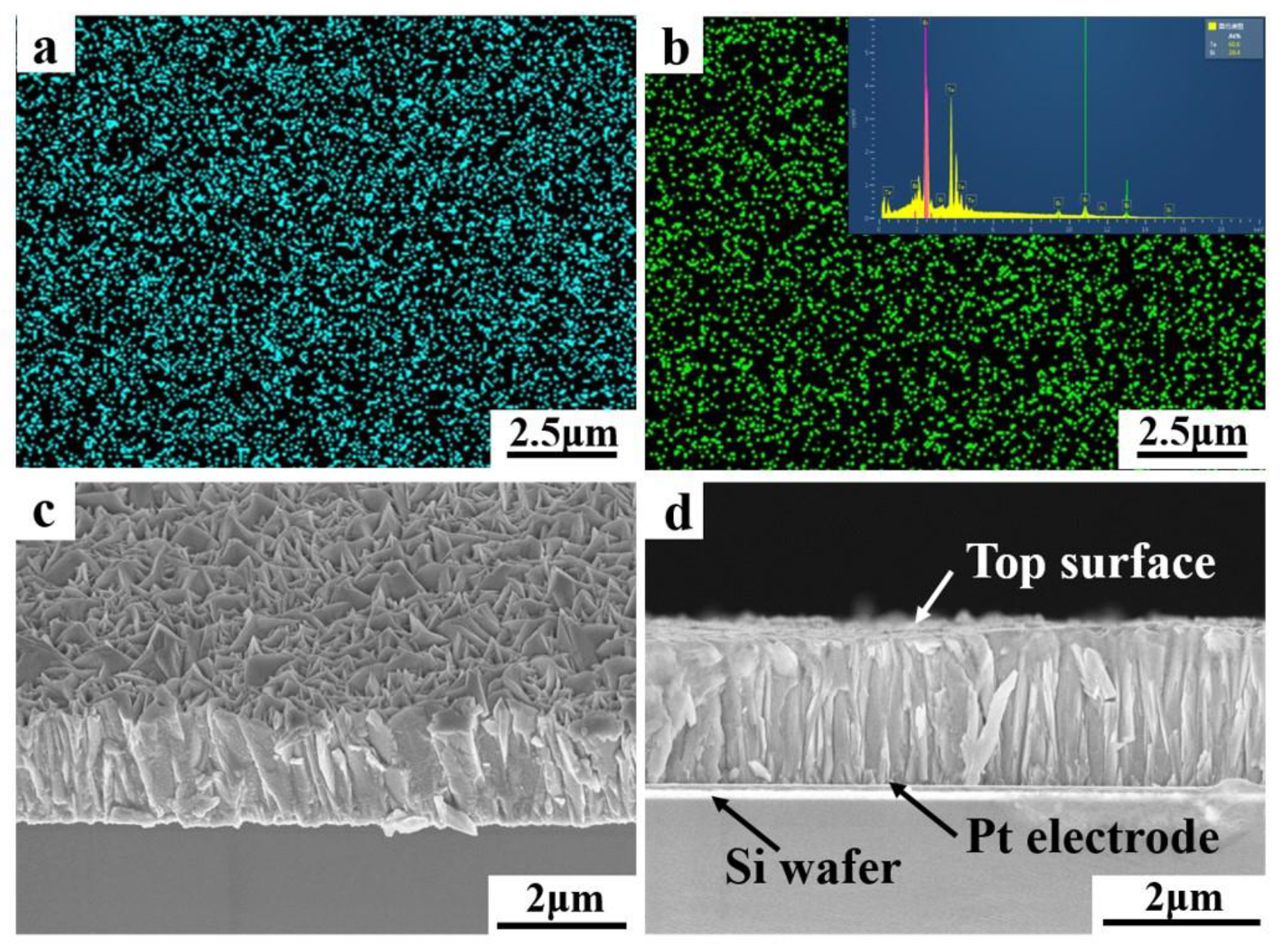
3.1. TE Film
3.2. TE Columns
4. Conclusions
Author Contributions
Funding
Conflicts of Interest
References
- Venkatasubramanian, R.; Siivola, E.; Colpitts, T.; O’Quinn, B. Thin-film thermoelectric devices with high room-temperature figures of merit. Nature 2001, 413, 597–602. [Google Scholar] [CrossRef] [PubMed]
- Bell, L.E. Cooling, heating, generating power, and recovering waste heat with thermoelectric systems. Science 2008, 321, 1457–1461. [Google Scholar] [CrossRef] [PubMed]
- Twaha, S.; Zhu, J.; Yan, Y.; Li, B. A comprehensive review of thermoelectric technology: Materials, applications, modelling and performance improvement. Renew. Sustain. Energy Rev. 2016, 65, 698–726. [Google Scholar] [CrossRef]
- Du, B.; Liu, M.; Xu, J.; Hu, B.; Liu, B.; Su, T.; Wang, J. Thermodynamic, Structural and Thermoelectric Properties of AgSbTe2 Thick Films Developed by Melt Spinning. Nanomaterials 2018, 8, 474. [Google Scholar] [CrossRef] [PubMed]
- Isotta, E.; Fanciulli, C.; Pugno, N.M.; Scardi, P. Effect of the Order-Disorder Transition on the Seebeck Coefficient of Nanostructured Thermoelectric Cu2ZnSnS4. Nanomaterials 2019, 9, 762. [Google Scholar] [CrossRef] [PubMed]
- Wang, J.; Mu, X.; Sun, M. The Thermal, Electrical and Thermoelectric Properties of Graphene Nanomaterials. Nanomaterials 2019, 9, 218. [Google Scholar] [CrossRef]
- Russ, B.; Glaudell, A.; Urban, J.J.; Chabinyc, M.L.; Segalman, R.A. Organic thermoelectric materials for energy harvesting and temperature control. Nat. Rev. Mater. 2016, 1. [Google Scholar] [CrossRef]
- Champier, D. Thermoelectric generators: A review of applications. Energy Convers. Manag. 2017, 140, 167–181. [Google Scholar] [CrossRef]
- Kraemer, D.; Jie, Q.; McEnaney, K.; Cao, F.; Liu, W.; Weinstein, L.A.; Loomis, J.; Ren, Z.; Chen, G. Concentrating solar thermoelectric generators with a peak efficiency of 7.4%. Nat. Energy 2016, 1, 1–8. [Google Scholar] [CrossRef]
- Blackburn, J.L.; Ferguson, A.J.; Cho, C.; Grunlan, J.C. Carbon-Nanotube-Based Thermoelectric Materials and Devices. Adv. Mater. 2018, 30. [Google Scholar] [CrossRef]
- Uda, K.; Seki, Y.; Saito, M.; Sonobe, Y.; Hsieh, Y.-C.; Takahashi, H.; Terasaki, I.; Homma, T. Fabrication of Pi-structured Bi-Te thermoelectric micro-device by electrodeposition. Electrochim. Acta 2015, 153, 515–522. [Google Scholar] [CrossRef]
- Shin, K.-J.; Oh, T.-S. Micro-Power Generation Characteristics of Thermoelectric Thin Film Devices Processed by Electrodeposition and Flip-Chip Bonding. J. Electron. Mater. 2015, 44, 2026–2033. [Google Scholar] [CrossRef]
- Ferrando-Villalba, P.; Pablo Perez-Marin, A.; Abad, L.; Goncalves Dalkiranis, G.; Lopeandia, A.E.; Garcia, G.; Rodriguez-Viejo, J. Measuring Device and Material ZT in a Thin-Film Si-Based Thermoelectric Microgenerator. Nanomaterials 2019, 9, 653. [Google Scholar] [CrossRef] [PubMed]
- Ma, Z.; Liu, Y.; Deng, L.; Zhang, M.; Zhang, S.; Ma, J.; Song, P.; Liu, Q.; Ji, A.; Yang, F.; et al. Heavily Boron-Doped Silicon Layer for the Fabrication of Nanoscale Thermoelectric Devices. Nanomaterials 2018, 8, 77. [Google Scholar] [CrossRef]
- He, R.; Schierning, G.; Nielsch, K. Thermoelectric Devices: A Review of Devices, Architectures, and Contact Optimization. Adv. Mater. Technol. 2018, 3. [Google Scholar] [CrossRef]
- Kim, T.Y.; Negash, A.; Cho, G. Direct contact thermoelectric generator (DCTEG): A concept for removing the contact resistance between thermoelectric modules and heat source. Energy Convers. Manag. 2017, 142, 20–27. [Google Scholar] [CrossRef]
- He, W.; Wang, S.; Li, Y.; Zhao, Y. Structural size optimization on an exhaust exchanger based on the fluid heat transfer and flow resistance characteristics applied to an automotive thermoelectric generator. Energy Convers. Manag. 2016, 129, 240–249. [Google Scholar] [CrossRef]
- Barry, M.M.; Agbim, K.A.; Rao, P.; Clifford, C.E.; Reddy, B.V.K.; Chyu, M.K. Geometric optimization of thermoelectric elements for maximum efficiency and power output. Energy 2016, 112, 388–407. [Google Scholar] [CrossRef]
- Su, Y.; Lu, J.; Huang, B. Free-standing planar thin-film thermoelectric microrefrigerators and the effects of thermal and electrical contact resistances. Int. J. Heat Mass Transf. 2018, 117, 436–446. [Google Scholar] [CrossRef]
- Poudel, B.; Hao, Q.; Ma, Y.; Lan, Y.; Minnich, A.; Yu, B.; Yan, X.; Wang, D.; Muto, A.; Vashaee, D.; et al. High-thermoelectric performance of nanostructured bismuth antimony telluride bulk alloys. Science 2008, 320, 634–638. [Google Scholar] [CrossRef]
- Hao, F.; Qiu, P.; Tang, Y.; Bai, S.; Xing, T.; Chu, H.-S.; Zhang, Q.; Lu, P.; Zhang, T.; Ren, D.; et al. High efficiency Bi2Te3-based materials and devices for thermoelectric power generation between 100 and 300 degrees C. Energy Environ. Sci. 2016, 9, 3120–3127. [Google Scholar] [CrossRef]
- Ruiz-Clavijo, A.; Caballero-Calero, O.; Martin-Gonzalez, M. Three-Dimensional Bi2Te3 Networks of Interconnected Nanowires: Synthesis and Optimization. Nanomaterials 2018, 8, 345. [Google Scholar] [CrossRef] [PubMed]
- Bai, X.; Ji, M.; Xu, M.; Su, N.; Zhang, J.; Wang, J.; Zhu, C.; Yao, Y.; Li, B. Synthesis of M- doped (M = Ag, Cu, In) Bi2Te3 nanoplates via a solvothermal method and cation exchange reaction. Inorg. Chem. Front. 2019, 6, 1097–1102. [Google Scholar] [CrossRef]
- Dharmaiah, P.; Hong, S.-J. Thermoelectric Properties of Bi2Te3 Nanocrystals with Diverse Morphologies Obtained via Modified Hydrothermal Method. J. Electron. Mater. 2017, 46, 3012–3019. [Google Scholar] [CrossRef]
- Peranio, N.; Eibl, O.; Nurnus, J. Structural and thermoelectric properties of epitaxially grown Bi2Te3 thin films and superlattices. J. Appl. Phys. 2006, 100. [Google Scholar] [CrossRef]
- Peranio, N.; Eibl, O.; Bassler, S.; Nielsch, K.; Klobes, B.; Hermann, R.P.; Daniel, M.; Albrecht, M.; Goerlitz, H.; Pacheco, V.; et al. From thermoelectric bulk to nanomaterials: Current progress for Bi2Te3 and CoSb3. Phys. Status Solidi A 2016, 213, 739–749. [Google Scholar] [CrossRef]
- Kim, K.-C.; Kwon, B.; Kim, H.J.; Baek, S.-H.; Hyun, D.-B.; Kim, S.K.; Kim, J.-S. Sn doping in thermoelectric Bi2Te3 films by metal-organic chemical vapor deposition. Appl. Surf. Sci. 2015, 353, 232–237. [Google Scholar] [CrossRef]
- Takayama, K.; Takashiri, M. Multi-layered-stack thermoelectric generators using p-type Sb2Te3 and n-type Bi2Te3 thin films by radio-frequency magnetron sputtering. Vacuum 2017, 144, 164–171. [Google Scholar] [CrossRef]
- Kim, H.-J.; Yim, J.-H.; Choi, W.C.; Park, C.; Kim, J.-S. The Effect of Annealing in Controlled Vapor Pressure on the Thermoelectric Properties of RF-Sputtered Bi2Te3 Film. J. Electron. Mater. 2012, 41, 1519–1523. [Google Scholar] [CrossRef]
- Sinnarasa, I.; Thimont, Y.; Presmanes, L.; Barnabe, A.; Tailhades, P. Thermoelectric and Transport Properties of Delafossite CuCrO2: Mg Thin Films Prepared by RF Magnetron Sputtering. Nanomaterials 2017, 7, 157. [Google Scholar] [CrossRef]
- Nguyen Huu, T.; Sakamoto, K.; Nguyen Van, T.; Ono, T. Synthesis and Evaluation of Thick Films of Electrochemically Deposited Bi2Te3 and Sb2Te3 Thermoelectric Materials. Materials 2017, 10, 154. [Google Scholar] [CrossRef]
- Pan, Y.; Wei, T.-R.; Wu, C.-F.; Li, J.-F. Electrical and thermal transport properties of spark plasma sintered n-type Bi2Te3-xSex alloys: The combined effect of point defect and Se content. J. Mater. Chem. C 2015, 3, 10583–10589. [Google Scholar] [CrossRef]
- Pan, Y.; Wei, T.-R.; Cao, Q.; Li, J.-F. Mechanically enhanced p- and n-type Bi2Te3-based thermoelectric materials reprocessed from commercial ingots by ball milling and spark plasma sintering. Mater. Sci. Eng. B Adv. Funct. Solid-State Mater. 2015, 197, 75–81. [Google Scholar] [CrossRef]
- Matsuo, H.; Yoshitoku, K.; Saito, M.; Takahashi, H.; Terasaki, I.; Homma, T. Fabrication of ZnO-Based Thermoelectric Micro-Devices by Electrodeposition. J. Electrochem. Soc. 2018, 165, D417–D422. [Google Scholar] [CrossRef]
- Snyder, G.J.; Lim, J.R.; Huang, C.K.; Fleurial, J.P. Thermoelectric microdevice fabricated by a MEMS-like electrochemical process. Nat. Mater. 2003, 2, 528–531. [Google Scholar] [CrossRef]
- Li, J.-F.; Tanaka, S.; Umeki, T.; Sugimoto, S.; Esashi, M.; Watanabe, R. Microfabrication of thermoelectric materials by silicon molding process. Sens. Actuators A Phys. 2003, 108, 97–102. [Google Scholar] [CrossRef]
- Lim, J.R.; Whitacre, J.F.; Fleurial, J.P.; Huang, C.K.; Ryan, M.A.; Myung, N.V. Fabrication method for thermoelectric nanodevices. Adv. Mater. 2005, 17, 1488–1492. [Google Scholar] [CrossRef]
- Martin, J.; Manzano, C.V.; Caballero-Calero, O.; Martin-Gonzalez, M. High-aspect-ratio and highly ordered 15-nm porous alumina templates. ACS Appl. Mater. Interfaces 2013, 5, 72–79. [Google Scholar] [CrossRef]
- Liu, D.-W.; Li, J.-F. Microfabrication of thermoelectric modules by patterned electrodeposition using a multi-channel glass template. J. Solid State Electrochem. 2011, 15, 479–484. [Google Scholar] [CrossRef]
- Su, N.; Guo, S.; Li, F.; Liu, D.; Li, B.; Li, J.; Ji, M. Micro-thermoelectric devices with large output power fabricated on a multi-channe glass template. J. Micromechanics Microengineering 2018, 28. [Google Scholar] [CrossRef]
- Martin-Gonzalez, M.S.; Prieto, A.L.; Gronsky, R.; Sands, T.; Stacy, A.M. Insights into the electrodeposition of Bi2Te3. J. Electrochem. Soc. 2002, 149, C546–C554. [Google Scholar] [CrossRef]
- Danaher, W.J.; Lyons, L.E. The Kinetics of the Electrodeposition of Cadmium Tellurdei. Aust. J. Chem. 1984, 37, 689–701. [Google Scholar] [CrossRef]
- Zhu, Y.-B.; Wang, W. Microstructure and thermoelectric properties of p-type Bi-Sb-Te-Se thin films prepared by electrodeposition method. Thin Solid Films 2012, 520, 2474–2478. [Google Scholar] [CrossRef]
- Michel, S.; Stein, N.; Schneider, M.; Boulanger, C.; Lecuire, J.M. Optimization of chemical and electrochemical parameters for the preparation of n-type Bi2Te3.7Se0.3 thin films by electrodeposition. J. Appl. Electrochem. 2003, 33, 23–27. [Google Scholar] [CrossRef]
- Song, Y.; Yoo, I.-J.; Heo, N.-R.; Lim, D.C.; Lee, D.; Lee, J.Y.; Lee, K.H.; Kim, K.-H.; Lim, J.-H. Electrodeposition of thermoelectric Bi2Te3 thin films with added surfactant. Curr. Appl. Phys. 2015, 15, 261–264. [Google Scholar] [CrossRef]
- Heo, P.; Hagiwara, K.; Ichino, R.; Okido, M. Electrodeposition and thermoelectric characterization of Bi2Te3. J. Electrochem. Soc. 2006, 153, C213–C217. [Google Scholar] [CrossRef]
- Kroger, F.A. Cathodic Deposition and Characterization of Metallic or Semiconducting Binary-alloys or Compounds. J. Electrochem. Soc. 1978, 125, 2028–2034. [Google Scholar] [CrossRef]
- Wu, Y.; Lin, Z.; Tian, Z.; Han, C.; Liu, J.; Zhang, H.; Zhang, Z.; Wang, Z.; Dai, L.; Cao, Y.; et al. Fabrication of Microstructured thermoelectric Bi2Te3 thin films by seed layer assisted electrodeposition. Mater. Sci. Semicond. Process. 2016, 46, 17–22. [Google Scholar] [CrossRef]
- Del Frari, D.; Diliberto, S.; Stein, N.; Boulanger, C.; Lecuire, J.M. Pulsed electrodeposition of (Bi1-xSbx)(2)Te-3 thermoelectric thin films. J. Appl. Electrochem. 2006, 36, 449–454. [Google Scholar] [CrossRef]
- Liu, D.-W.; Li, J.-F. Electrocrystallization process during deposition of Bi-Te films. J. Electrochem. Soc. 2008, 155, D493–D498. [Google Scholar] [CrossRef]
- Huang, B.-L.; Kaviany, M. Ab initio and molecular dynamics predictions for electron and phonon transport in bismuth telluride. Phys. Rev. B 2008, 77. [Google Scholar] [CrossRef]
- Manzano, C.V.; Abad, B.; Munoz Rojo, M.; Koh, Y.R.; Hodson, S.L.; Lopez Martinez, A.M.; Xu, X.; Shakouri, A.; Sands, T.D.; Borca-Tasciuc, T.; et al. Anisotropic Effects on the Thermoelectric Properties of Highly Oriented Electrodeposited Bi2Te3 Films. Sci. Rep. (UK) 2016, 6. [Google Scholar] [CrossRef] [PubMed]
- Zahn, P.; Hinsche, N.F.; Yavorsky, B.Y.; Mertig, I. Bi2Te3: Implications of the rhombohedral k-space texture on the evaluation of the in-plane/out-of-plane conductivity anisotropy. J. Phys. Condens. Mat. 2011, 23. [Google Scholar] [CrossRef] [PubMed]
- Yavorsky, B.Y.; Hinsche, N.F.; Mertig, I.; Zahn, P. Electronic structure and transport anisotropy of Bi2Te3 and Sb2Te3. Phys. Rev. B 2011, 84. [Google Scholar] [CrossRef]
- Fei, J.-Y.; Wilcox, G. Electrodeposition of Zn–Co alloys with pulse containing reverse current. Electrochim. Acta 2005, 50, 2693–2698. [Google Scholar] [CrossRef]
- Chandrasekar, M.; Pushpavanam, M. Pulse and pulse reverse plating—Conceptual, advantages and applications. Electrochim. Acta 2008, 53, 3313–3322. [Google Scholar] [CrossRef]
- Liu, D.-W.; Xu, Y.; Li, J.-F. Electrodeposition of Bi2Te3 films and micro-pillar arrays on p-Si(100) wafers. Phys. Status Solidi A 2010, 207, 354–359. [Google Scholar] [CrossRef]
- Schumacher, C.; Reinsberg, K.G.; Akinsinde, L.; Zastrow, S.; Heiderich, S.; Toellner, W.; Rampelberg, G.; Detavernier, C.; Broekaert, J.A.C.; Nielsch, K.; et al. Optimization of Electrodeposited p-Doped Sb2Te3 Thermoelectric Films by Millisecond Potentiostatic Pulses. Adv. Energy Mater. 2012, 2, 345–352. [Google Scholar] [CrossRef]
- Zou, Z.G.; Cai, K.F.; Chen, S.; Qin, Z. Pulsed electrodeposition and characterization of Bi2Te3-ySey films. Mater. Res. Bull. 2012, 47, 3292–3295. [Google Scholar] [CrossRef]


© 2020 by the authors. Licensee MDPI, Basel, Switzerland. This article is an open access article distributed under the terms and conditions of the Creative Commons Attribution (CC BY) license (http://creativecommons.org/licenses/by/4.0/).
Share and Cite
Su, N.; Guo, S.; Li, F.; Li, B. Electrodeposition of Bi-Te Thin Films on Silicon Wafer and Micro-Column Arrays on Microporous Glass Template. Nanomaterials 2020, 10, 431. https://doi.org/10.3390/nano10030431
Su N, Guo S, Li F, Li B. Electrodeposition of Bi-Te Thin Films on Silicon Wafer and Micro-Column Arrays on Microporous Glass Template. Nanomaterials. 2020; 10(3):431. https://doi.org/10.3390/nano10030431
Chicago/Turabian StyleSu, Ning, Shuai Guo, Fu Li, and Bo Li. 2020. "Electrodeposition of Bi-Te Thin Films on Silicon Wafer and Micro-Column Arrays on Microporous Glass Template" Nanomaterials 10, no. 3: 431. https://doi.org/10.3390/nano10030431
APA StyleSu, N., Guo, S., Li, F., & Li, B. (2020). Electrodeposition of Bi-Te Thin Films on Silicon Wafer and Micro-Column Arrays on Microporous Glass Template. Nanomaterials, 10(3), 431. https://doi.org/10.3390/nano10030431