Article

A Tunable Triple-Band Near-Infrared Metamaterial Absorber Based on Au Nano-Cuboids Array

1
Joint Laboratory for Extreme Conditions Matter Properties, Southwest University of Science and Technology, Mianyang 621010, China
2
Research Center for Photonic Technology, Fujian Key Laboratory for Advanced Micro-nano Photonics Technology and Devices & Key Laboratory of Information Functional Material for Fujian Higher Education, Quanzhou Normal University, Fujian 362000, China
3
State Key Laboratory of Advanced Processing and Recycling of Non-ferrous Metals, Lanzhou University of Technology, Lanzhou 730050, China
4
Key Laboratory of Metallurgical Equipment and Control Technology of Ministry of Education, Wuhan University of Science and Technology, Wuhan 430081, China
5
College of Physics and Electronics, Central South University, Changsha 410083, China
*
Authors to whom correspondence should be addressed.
These authors contribute equally to this article.
Nanomaterials 2020, 10(2), 207; https://doi.org/10.3390/nano10020207
Submission received: 20 December 2019 / Revised: 10 January 2020 / Accepted: 16 January 2020 / Published: 24 January 2020

Abstract

:
In this article, we present a design for a triple-band tunable metamaterial absorber with an Au nano-cuboids array, and undertake numerical research about its optical properties and local electromagnetic field enhancement. The proposed structure is investigated by the finite-difference time domain (FDTD) method, and we find that it has triple-band tunable perfect absorption peaks in the near infrared band (1000–2500 nm). We investigate some of structure parameters that influence the fields of surface plasmons (SP) resonances of the nano array structure. By adjusting the relevant structural parameters, we can accomplish the regulation of the surface plasmons resonance (SPR) peaks. In addition, the triple-band resonant wavelength of the absorber has good operational angle-polarization-tolerance. We believe that the excellent properties of our designed absorber have promising applications in plasma-enhanced photovoltaic, optical absorption switching and infrared modulator optical communication.

Graphical Abstract

1. Introduction

In recent years, there has been a great development of surface plasmons, which is an electromagnetic wave propagating along the interface between a medium and metal. It is generated by coupling the light field and collective electron oscillation on the metal surface [1,2,3,4,5]. Surface plasmons play an extremely important role in optical wave guides, optical absorption switches, subwavelength optics, sensors, and photocatalysis [6,7,8,9,10,11,12,13,14,15]. Local surface plasmon resonance is an important branch of the surface plasmon field. In particular, the local surface plasmon resonance (LSPR) of Au nanoparticles (NPs) has received extensive attention for many years due to its unique optical properties [16,17,18]. Under the action of incident light, the collective oscillation of Au free electrons can enhance the local electromagnetic field on their surface [19]. Au nanoparticles have strong local electromagnetic field enhancement on the surface, which has been widely used in fields such as catalysis, photonics, sensing and surface enhanced Raman scattering (SERS) [20,21,22,23,24,25].
The perfect metamaterial absorbers (MAs) have the ability to absorb incident waves and the property of almost perfect absorption. Moreover, it has some special properties in nature, such as perfect lens, stealth, and negative refractive index [26,27,28], which has attracted wide attention. Metamaterials are composite arrays of subwavelength resonant metal structures with specific optical properties. In 2008, Landy et al. first proposed a perfect absorption material based on a metal structure, which is composed of metal–electrolyte–metal [29]. Due to the strong resonance of metal structures, the absorption rate is almost perfect. The properties of metamaterials depend on the geometry of a single cell. In recent years, people have conducted in-depth studies on the design, preparation and characterization of MAs [30,31,32,33,34,35,36]. Metamaterials have developed from microwave to terahertz, infrared and visible regions [37,38,39,40], and from single band and polarization sensitivity to multiband and weak polarization sensitivity [41,42,43,44]. However, currently existing MAS are mostly single-band, sensitive to polarization and have low tolerance to incident angle, which requires the design of a metamaterial absorber with multiband, insensitive polarization and wide angle.
In recent years, optical absorption studies have been performed on multi-band metamaterial absorbers. For example, Wang et al. explored the absorption rate of triple-band metamaterial [45], but the peak tunability is poor and the sensitivity to angle and polarization is relatively high. In this paper, we address these shortcomings and design a triple-band tunable metamaterial absorber. We adopt the finite-difference time-domain (FDTD) method, and research absorption characteristics and resonance sensitivity to light. We find that the three peaks in the absorption spectrum are caused by resonance effect and surface-based plasmon resonance. The peak can be adjusted by changing the structural parameters of the model and the background environment, and the structure has the advantage of being insensitive to angle and polarization. Therefore, the triple-band tunable ideal metamaterial absorber designed by our team will have potential applications in the fields of plasmon-enhanced photovoltaic, optical absorption switch and infrared modulation optical communication.

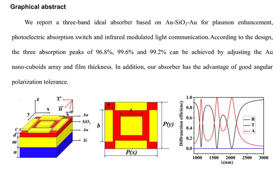
2. Structure Design and Numerical Model

In the numerical calculation, Wang et al. used FDTD to calculate the optical properties of the absorber, and we also used the same technique for numerical simulation [46,47]. We numerically analyzed the performance and the optical response of the plasma nanostructures by employing the FDTD simulations. We propose a structure of the tunable triple-band absorber concentrating near the near infrared region as shown in Figure 1. We consider that the metamaterial designed in the top panel contains a square matrix. Gold was chosen as a metallic element for its chemical stability and low ohmic loss. The structure made up of a Au nano-cuboids array. The Drude model is a simulation model that is closer to the experimental item than many other models. For example, Wang et al. used the Drude model to study related absorbers [45]. The dielectric constant of Au can be calculated by using the Drude model [48,49,50], which works well in the near infrared band. The Drude formula is
ε ( ω ) = ε ω p 2 ω 2 + i γ c ω
where ωp is the plasma frequency, and γc is the damping constant. For Au, ε = 9.1, γc = 4.05 × 10¹³ rad/s, and ωp = 1.38 × 10¹⁶ rad/s [51,52]. The complex refractive index data of Si is taken from Palik [53]. In the metal rectangular plate, t represents the length of the side of the rectangular plate with equal sides. b and a respectively represent the long side and the short side of the rectangle with unequal sides. During each period, the rectangular plates with equilateral edges are located in the center and the four rectangular plates with unequal edges are located in the four directions of the period. The change in the size of the rectangular plate resonator allows the effective dielectric constant and permeability to be specified. These dielectric constants and permeability provide impedance-matching to minimize reflection. Due to the resonance of the local surface of Au nanoparticles, our absorber can achieve triple-band spectral tuning by adjusting the structure. In the calculation, the plane wave source is polarized along the x direction. To reduce computation time and server memory, we consider periodic boundary conditions in the x and y directions. The perfect matching layer can be directly adopted in the z direction outside the structure area. We set the mesh precision to a higher level of 6, and the plane light source used is from 0.9 to 3 µm. The Au nano-cuboids array has the same length along the x and y directions. The geometric parameters of the structure are set as follows: upper Au thickness c = 25 nm, dielectric layer SiO2, dielectric layer d = 35 nm, lower Au film thickness m = 200 nm, substrate SiO2 thickness n = 300 nm, t = 300 nm, b = 400 nm, a = 90 nm, P(x) = P(y) = 600 nm. The absorber we designed is simple in structure, and the preparation process in the experiment is simple and easy to realize.

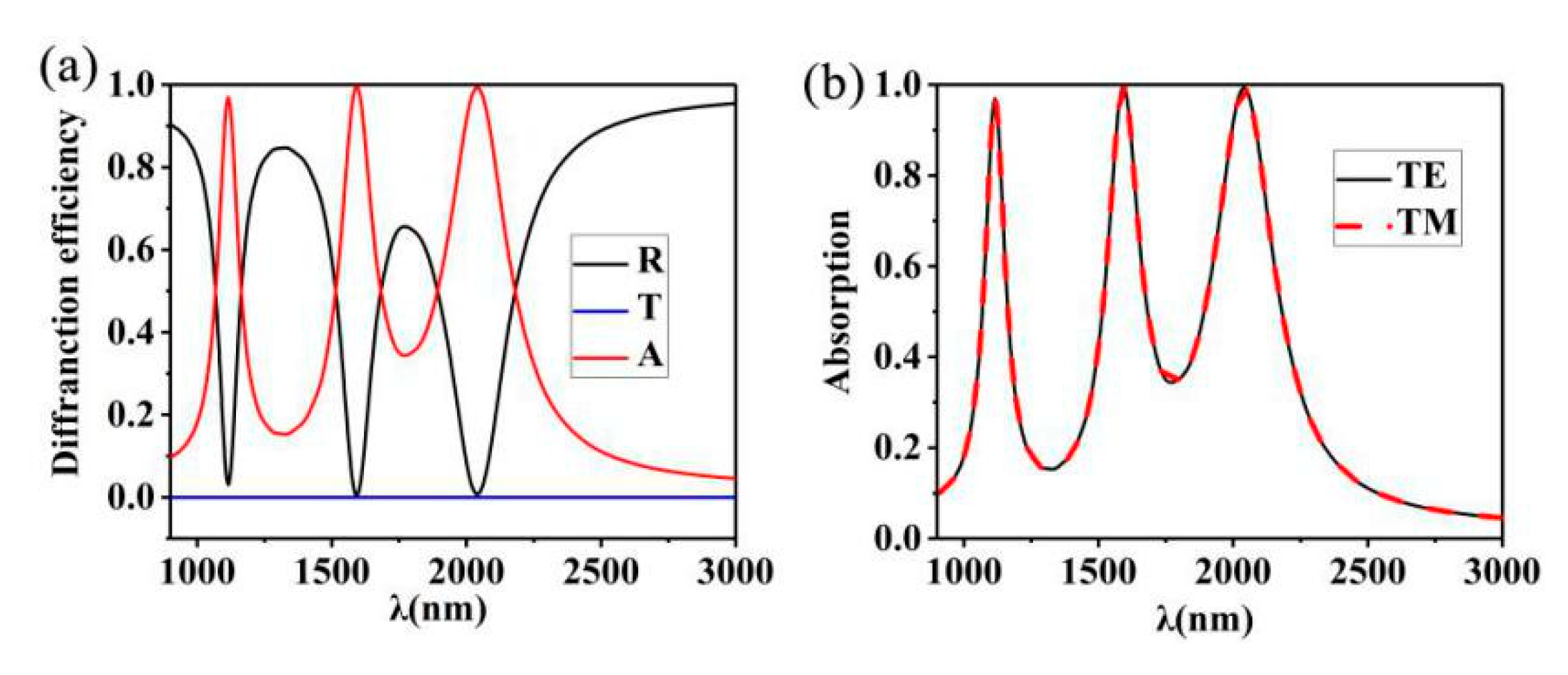
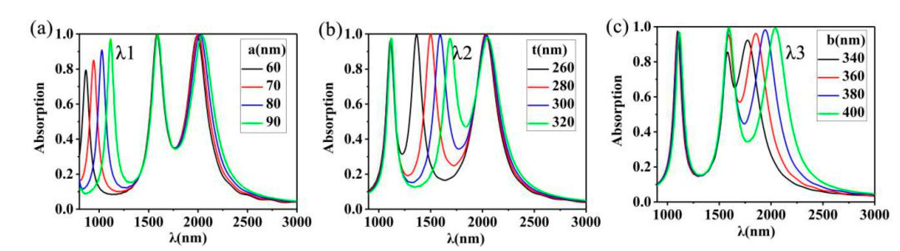
3. Simulations Results and Discussions

We calculate reflectivity (R) and transmittance (T) in detail, and then define absorption rate A in terms of 1-T-R [54,55,56,57,58]. The simulation results of the unit units of the proposed nanostructure in the wavelength range of 900–3000 nm are shown in Figure 2a. In the calculation, the plane wave source is polarized along the x direction. It can be concluded that in the near infrared range, the transmission quantity is significantly less than 0.01. This is because the thickness of the Au film is greater than the depth of the incident light. The reflection spectrum presents a narrow dip angle at the wavelengths of 1115 nm, 1593 nm and 2039 nm, respectively. The reason for the dip angle of the narrow band is that when the incident light field is incident on the Au nano-cuboids array structure, plasmon resonance will appear in the upper and lower parts of the Au nano-cuboids array, and this plasmon resonance will appear at the three peaks. It can be seen from Figure 2b that since the structure presents periodicity in the direction of TE and TM, this triple-band absorber is insensitive to TE and TM waves.
To evaluate the performance excellence of the proposed structure, we compared the results with other similar absorbers structures with three peaks listed in Table 1. From the table, we can see that two of our peak values are more than 99%, while the others contain at most one. Although our structure is not the highest when comparing the highest peaks, the average peak of the structure we designed is higher than the average absorption peak of other similar structures. It is clear the absorption efficiency of our designed absorber is better than that of the other absorbers in Table 1.
In order to better explain the three perfect absorption peaks in the structure we designed previously, we conducted decomposition analysis of the structure. As shown in Figure 3, this is the absorption spectrum diagram of cuboid configurations with different Au nano-particles, and it obtains the response of three bands. According to the simulation results in Figure 3b, when the electric field component of the light source is along the direction of TE, the Au nano-cuboids array at the center shows a peak value at 1581 nm. In one period, a peak value was also found on the long side of the marginal cubic structure along the direction of TE, and on the short side of the marginal cubic structure along the direction of TE. It is worth noting that in the simulation, polarized electric field exists along this direction, so we choose to place four rectangular symmetric points. The Au nano-cuboid array is arranged in one period. Meanwhile, we simulate the absorption spectrum of the whole model by maintaining the incident polarization. As can be seen from Figure 3d, the green line is compared with the lines of other colors: the three peaks all show a slight blue shift; it is worth noting that the green line has a much higher peak than the black line (from 0.87 to 0.97), this is because the structure of the surface plasmon resonance peak and part of the plasma enhanced effect appears. Since the three peaks all correspond to each other, we can determine that the absorption spectra of the three bands are composed by Figure 4a–c.
In addition, in order to better understand the physical mechanism of peaks, we calculate the Figure 3a–c the corresponding electric diagram in the XOY plane. In Figure 4a–c, by comparing the two figures find that when the peak at 1084 nm, a peak perpendicular to the long side of the X-axis cube resonance formed. When the peak is at 1581 nm, the peak is formed by the resonance of the middle cube. The other dipole plasma resonance was found to be generated by the short side of the cube perpendicular to the X-axis at 1985 nm. At the same time, we also calculate the electromagnetic field intensity distribution at different resonant wavelengths (λ1 = 1115 nm, λ2 = 1593 nm, λ3 = 2039 nm) in the XOY plane (Figure 4d–f). As shown in Figure 4e, the peak at 1115 nm by complete perpendicular to the x-axis of the cube long edge to the formation of resonance. Similarly, the peak at 1593 nm is basic caused by the resonance of the intermediate cube, the peak at 2039 nm is basic caused by the short side resonance of the cube perpendicular to the x-axis; this also further confirmed that the peak value of the three sources are respectively formed by the separate cube resonance. It is noteworthy that the resonance effect of Figure 4e–f is stronger than that of Figure 4a–c, which is caused by the interaction between the cube resonance during this period. Meanwhile, we calculate the electromagnetic field intensity distribution at different resonant wavelengths (λ1 = 1115 nm, λ2 = 1593 nm, λ3 = 2039 nm) in the XOZ plane. It can be seen from Figure 4g–i that the strong electromagnetic field is mainly concentrated between the Au/SiO2 interface and the air/metal nano-cube at the top. Under the action of incident plane waves, it can be seen from Figure 4g that the strong electromagnetic field is excited by the Au cube and SiO2 on both sides, while in Figure 4h, the excitation is mainly caused by the interaction between the Au cube, SiO2 and air. For λ3, it is not difficult to see the interaction between the Au cube and SiO2 under the action of incident waves through Figure 4i. From Figure 4, it can be concluded that the surface plasmon polaritons’ (SPPs) resonance and Fabry-Pero resonance show that there will be a strong electromagnetic field distribution near the nano scale groove [61,62,63].
We also explored the effects of different parameters on the absorption of the Au nano-cuboids array, as shown in Figure 5b; t = 260 nm (black), t = 280 nm (red), t = 300 nm (blue), t = 320 nm (green). Due to the close proximity of the Au nano-cuboids array, the coupling effect may affect our absorption performance. Therefore, we selected the changes of fixed geometric parameters that will affect resonance. First, we fixed the parameters of the surrounding cube within the period, a = 90 nm and b = 40 nm, and changed the side length of the middle cube in the period, as shown in Figure 5b. As t increases from 260 to 320 nm, the corresponding resonance peak showed obvious red shift (λ2: from 1358 to 1658 nm). Then, as shown in Figure 5a, by changing the value of side length a, we can clearly see that λ1 varies from (863, 0.78), (943, 0.84), (1027, 0.90) to (1111, 0.96). The peak value shows obvious red shift and rise and presents a linear relationship. As shown in Figure 5c, by changing the value of side length b, we can see that λ3 changes from (1772, 0.92), (1584, 0.96), (1940, 0.98) to (2039, 0.99), and the peak value shows obvious red shift and rise. It can only be noted that there is a certain increase in the peak value of λ2 here (from 0.85 to 0.99), which is due to resonance. These indicate that we can adjust the position and height of the three peaks by changing the structure so that we can use them as tunable metal elements such as optical absorption switches and optical modulators [64,65,66].
The effects of the thickness of the dielectric layer and the thickness of the Au nano-cuboids array on the absorption spectrum were also studied. The results are as shown in Figure 6, through preliminary observation, we can find that changing the thickness of dielectric layer c and changing the thickness of top layer d have very similar effects on our absorption rate. There is a slight blue shift and a decrease in the peak value of λ1, λ1 in Figure 6a from (1185, 0.99) to (1079, 0.89), and λ1 in Figure 6b from (1167, 0.99) to (1084, 0.94). For λ2, there is a blue shift and a decrease in the peak value of λ2. λ2 in Figure 6a from (1716, 0.93) to (1540, 0.99), and λ2 in Figure 6b from (1697, 0.93) to (1542, 0.99). For λ3, blue shift occurs. It is worth noting that the peak value of λ3 increases first and then decreases as the value of c or d changes. With the characteristics of the medium layer and top metal, we can also make tunable metal elements.
However, for many metal absorbers, once their structures are fixed, their resonant wavelengths will no longer be tunable, so we calculated the change of absorption spectrum in different background environments. Figure 7a shows the absorption spectra of n = 1.0, n = 1.1, n = 1.2, and n = 1.3 with wavelengths of 900–3000 nm. The phenomenon of red shift appears with the increase of the ambient refractive index by three peaks. λ1 from 1115 nm to 1190 nm, λ2 from 1593 to 1743 nm, λ3 from 2093 to 2224 nm. It can also be seen from Figure 7b that the redshifts of the three absorption peaks vary linearly from 1.0 to 1.3 in the background environment. Therefore, this resonance mode of our designed absorber can be used to adjust our absorber to achieve the desired effect in different environments.
It is well known that in practical applications it is very important for devices to be insensitive to angle and polarization [67,68,69]. Therefore, we performed additional simulation calculations to study the effects of angle and polarization on triple-band absorbent materials. It can be seen from Figure 8a,b that when the incidence angle reaches 40°, the perfect absorption is almost uninterrupted while keeping the central wavelength unchanged. This means that these strong absorbents are weak depending on polarization and incidence angle. This is because the Au nano-cuboids array we designed has good symmetry and can be completely absorbed by the absorber. The above results show that the triple-band tunable ideal absorber with nanostructured Au has a good angular polarization tolerance, which overcomes one of the shortcomings of the former absorber.

4. Conclusions

In conclusion, we designed a triple-band metamaterial absorber which is weakly dependent on polarization and incident angle. It consists of three layers of thin films called Au–SiO2–Au. Through the numerical calculation of the absorber, the results show that due to the Fabry–Pero resonance effect, the strong field is localized in SiO2 in the dielectric layer. The SiO2 layer limits the action of the electromagnetic field. The results show that the three absorption peaks of 96.8%, 99.6% and 99.2% can be achieved by adjusting the Au nano-cuboids array and film thickness. In addition, our absorber has the advantage of a good angular polarization tolerance. Through the reasonable design of the geometric structure of the device, the device can be used in the near-infrared resonance absorption wavelength. The results show that the periodic tunable triple-band metamaterial absorber has the advantages of perfect absorption, insensitivity to angle and polarization, and it can be widely used in plasma enhancement photoelectric, light absorption switch, infrared modulation light communication and other fields.

Author Contributions

Conceptualization, F.Q., Z.C., and Z.Y.; data curation, F.Q., Z.C., and X.C.; formal analysis, Z.Y., W.Y., T.D., P.W., and H.Y.; methodology, H.Y., G.L., and Y.Y.; resources, P.W.; software, P.W., Z.C., Y.Y., X.C., and G.L.; data curation, F.Q.; writing—original draft preparation, F.Q.; writing—review and editing, F.Q., Z.C., Z.Y., W.Y., and Y.Y. All authors have read and agreed to the published version of the manuscript.

Funding

This research received no external funding.

Acknowledgments

This research was funded by the National Natural Science Foundation of China (NNSFC), grant numbers 51606158, 11604311, 61705204, 21506257, 11604091, 11547186, and 51575407; funded by the Natural Science Foundation of Fujian Province, grant number 2018J05008 and JZ160459; funded by Sichuan Science and Technology Program, grant number 2018GZ0521; Funded by PhD Research Startup Foundation of Quanzhou Normal University (G16057); and funded by the Distinguished Young Scholars Program of Fujian Province (C18032).

Conflicts of Interest

The authors declare no conflicts of interest.

References

  1. Wang, Y.Y.; Qin, F.; Yi, Z.; Chen, X.F.; Zhou, Z.G.; Yang, H.; Liao, X.; Tang, Y.J.; Yao, W.T.; Yi, Y.G. Effect of slit width on surface plasmon resonance. Results Phys. 2019, 15, 102711. [Google Scholar] [CrossRef]
  2. Liang, C.P.; Yi, Z.; Chen, X.F.; Tang, Y.J.; Yi, Y.; Zhou, Z.G.; Wu, X.G.; Huang, Z.; Yi, Y.G.; Zhang, G.F. Dual-band infrared perfect absorber based on a Ag-dielectric-Ag multilayer films with nanoring grooves arrays. Plasmonics 2019. [Google Scholar] [CrossRef]
  3. He, Z.H.; Zhao, J.L.; Lu, H. Tunable nonreciprocal reflection and its stability in a non-PT-symmetric plasmonic resonators coupled waveguide systems. Appl. Phys. Express 2020, 13, 012009. [Google Scholar] [CrossRef]
  4. Wang, X.X.; Zhu, J.K.; Tong, H.; Yang, X.D.; Wu, X.X.; Pang, Z.Y.; Yang, H.; Qi, Y.P. A theoretical study of a plasmonic sensor comprising a gold nano-disk array on gold film with an SiO2 spacer. Chin. Phys. B 2019, 28, 044201. [Google Scholar] [CrossRef]
  5. Li, Y.; Liu, Z.; Zhang, H.; Tang, P.; Wu, B.; Liu, G. Ultra-broadband perfect absorber utilizing refractory materials in metal-insulator composite multilayer stacks. Optics Express 2019, 27, 11809–11818. [Google Scholar] [CrossRef]
  6. Yan, Y.X.; Yang, H.; Yi, Z.; Xian, T. NaBH4-reduction induced evolution of Bi nanoparticles from BiOCl nanoplates and construction of promising Bi@BiOCl hybrid photocatalysts. Catalysts 2019, 9, 795. [Google Scholar] [CrossRef] [Green Version]
  7. Wang, Y.P.; Yang, H.; Sun, X.F.; Zhang, H.M.; Xian, T. Preparation and photocatalytic application of ternary n-BaTiO3/Ag/p-AgBr heterostructured photocatalysts for dye degradation. Mater. Res. Bull. 2020, 124, 110754. [Google Scholar] [CrossRef]
  8. Guan, S.T.; Yang, H.; Sun, X.F.; Xian, T. Preparation and promising application of novel LaFeO3/BiOBr heterojunction photocatalysts for photocatalytic and photo-Fenton removal of dyes. Opt. Mater 2020, 100, 109644. [Google Scholar] [CrossRef]
  9. Yan, Y.X.; Yang, H.; Yi, Z.; Xian, T.; Wang, X.X. Direct Z-scheme CaTiO3@BiOBr composite photocatalysts with enhanced photodegradation of dyes. Sci. Pollut. Res. 2019, 26, 29020–29031. [Google Scholar] [CrossRef]
  10. Wang, S.Y.; Yang, H.; Yi, Z.; Wang, X.X. Enhanced photocatalytic performance by hybridization of Bi2WO6 nanoparticles with honeycomb-like porous carbon skeleton. J. Environ. Manag. 2019, 248, 109341. [Google Scholar] [CrossRef]
  11. Gao, H.J.; Zheng, C.X.; Yang, H.; Niu, X.W.; Wang, S.F. Construction of a CQDs/Ag3PO4/BiPO4 heterostructure photocatalyst with enhanced photocatalytic degradation of rhodamine B under simulated solar irradiation. Micromachines 2019, 10, 557. [Google Scholar] [CrossRef] [PubMed] [Green Version]
  12. Li, H.L.; Wang, G.Y.; Niu, J.B.; Wang, E.L.; Niu, G.; Xie, C.Q. Preparation of TiO2 nanotube arrays with efficient photocatalytic performance and super-hydrophilic properties utilizing anodized voltage method. Results Phys. 2019, 14, 102499. [Google Scholar] [CrossRef]
  13. Yi, Z.; Li, X.; Wu, H.; Chen, X.F.; Yang, H.; Tang, Y.J.; Yi, Y.G.; Wang, J.Q.; Wu, P.H. Fabrication of ZnO@Ag3PO4 Core-Shell nanocomposite arrays as photoanodes and their photoelectric properties. Nanomaterials 2019, 9, 1254. [Google Scholar] [CrossRef] [PubMed] [Green Version]
  14. Yi, Z.; Zeng, Y.; Wu, H.; Chen, X.F.; Fan, Y.X.; Yang, H.; Tang, Y.J.; Yi, Y.G.; Wang, J.Q.; Wu, P.H. Synthesis, surface properties, crystal structure and dye-sensitized solar cell performance of TiO2 nanotube arrays anodized under different parameters. Results Phys. 2019, 15, 102609. [Google Scholar] [CrossRef]
  15. Liao, M.; Wu, L.F.; Zhang, Q.B.; Dai, J.Y.; Yao, W.T. Controlled morphology of single-crystal molybdenum trioxide nanobelts for photocatalysis. J. Nanosci. Nanotechnol. 2020, 20, 1917–1921. [Google Scholar] [CrossRef] [PubMed]
  16. Yu, P.Q.; Chen, X.F.; Yi, Z.; Tang, Y.J.; Yang, H.; Zhou, Z.G.; Duan, T.; Cheng, S.B.; Zhang, J.G.; Yi, Y.G. A numerical research of wideband solar absorber based on refractory metal from visible to near infrared. Opt. Mater 2019, 97, 109400. [Google Scholar] [CrossRef]
  17. Wu, P.H.; Chen, Z.Q.; Xu, D.Y.; Zhang, C.F.; Jian, R.H. A narrow dual-band monolayer unpatterned graphene-based perfect absorber with critical coupling in the near infrared. Micromachines 2020, 11, 58. [Google Scholar] [CrossRef] [Green Version]
  18. Liu, Q.; Yan, B.; Liu, J. U-shaped photonic quasi-crystal fiber sensor with high sensitivity based on surface plasmon resonance. Appl. Phys. Express 2019, 12, 052014. [Google Scholar] [CrossRef]
  19. Wang, X.X.; Zhu, J.K.; Wen, X.L.; Wu, X.X.; Wu, Y.; Su, Y.W.; Tong, H.; Qi, Y.P.; Yang, H. Wide range refractive index sensor based on a coupled structure of Au nanocubes and Au film. Opt. Mater. Express 2019, 9, 3079–3088. [Google Scholar] [CrossRef]
  20. Wang, X.X.; Bai, X.L.; Pang, Z.Y.; Zhu, J.K.; Wu, Y.; Yang, H.; Qi, Y.P.; Wen, X.L. Surface-enhanced Raman scattering by composite structure of gold nanocube-PMMA-gold film. Opt. Mater. Express 2019, 9, 1872–1881. [Google Scholar] [CrossRef]
  21. Wang, W.; Zhao, Z.H.; Guo, C.; Guo, K.; Guo, Z.Y. Spin-selected Dual-wavelength plasmonic metalenses. Nanomaterials 2019, 9, 761. [Google Scholar] [CrossRef] [PubMed] [Green Version]
  22. Shi, D.; Xiong, Z.; Li, J.; Luo, B.; Fang, L.; Xia, Y.; Gao, Z. Electron transition and electron-hole recombination processes in epitaxial BaTiO3 films with embedded Co nanocrystals. Mater. Res. Express 2019, 6, 105021. [Google Scholar] [CrossRef]
  23. Han, S.B.; Zhu, Y.M.; Cai, C.; Zhu, J.K.; Han, W.B.; Chen, L.; Zu, X.T.; Yang, H.; Gu, M. Failure mechanism of Au@Co9S8 yolk-shell anode in Li-ion batteries unveiled by in-situ transmission electron microscopy. Appl. Phys. Lett. 2019, 114, 113901. [Google Scholar] [CrossRef]
  24. Cheng, Y.; Du, C. Broadband plasmonic absorber based on all silicon nanostructure resonators in visible region. Opt. Mater 2019, 98, 109441. [Google Scholar] [CrossRef]
  25. Chen, J.; Fan, W.F.; Mao, P.; Tang, C.J.; Liu, Y.J.; Yu, Y.; Zhang, L.B. Tailoring plasmon lifetime in suspended nanoantenna arrays for high-performance plasmon sensing. Plasmonics 2017, 12, 529–534. [Google Scholar] [CrossRef]
  26. Cen, C.L.; Zhang, Y.B.; Chen, X.F.; Yang, H.; Yi, Z.; Yao, W.T.; Tang, Y.J.; Yi, Y.G.; Wang, J.Q.; Wu, P.H. A dual-band metamaterial absorber for graphene surface plasmon resonance at terahertz frequency. Phys. E 2020, 117, 113840. [Google Scholar] [CrossRef]
  27. Li, H.L.; Niu, J.B.; Wang, G.Y. Dual-band, polarization-insensitive metamaterial perfect absorber based on monolayer graphene in the mid-infrared range. Results Phys. 2019, 13, 102313. [Google Scholar] [CrossRef]
  28. Liu, E.; Tan, W.; Yan, B.; Xie, J.; Ge, R.; Liu, J. Robust transmission of orbital angular momentum mode based on a dual-cladding photonic quasi-crystal fiber. J. Phys. D Appl. Phys 2019, 52, 325110. [Google Scholar] [CrossRef]
  29. Landy, N.I.; Sajuyigbe, S.; Mock, J.J.; Smith, D.R.; Padilla, W.J. Perfect metamaterial absorber. Phys. Rev. Lett. 2008, 100, 207–402. [Google Scholar] [CrossRef]
  30. Liu, C.; Su, W.Q.; Wang, F.M.; Li, X.L.; Yang, L.; Sun, T.; Mu, H.W.; Chu, P.K. Theoretical assessment of a highly sensitive photonic crystal fibre based on surface plasmon resonance sensor operating in the near-infrared wavelength. J. Mod. Opt. 2019, 66, 1–6. [Google Scholar] [CrossRef]
  31. Wang, X.X.; Wu, X.X.; Zhu, J.K.; Pang, Z.Y.; Yang, H.; Qi, Y.P. Theoretical investigation of a highly sensitive refractive-index sensor based on TM0 waveguide mode resonance excited in an asymmetric metal-cladding dielectric waveguide structure. Sensors 2019, 19, 1187. [Google Scholar] [CrossRef] [PubMed] [Green Version]
  32. Liu, Z.Q.; Tang, P.; Liu, X.S.; Yi, Z.; Liu, G.Q.; Wang, Y.; Liu, M.L. Truncated titanium/semiconductor cones for wide-band solar absorbers. Nanotechnology 2019, 30, 305203. [Google Scholar] [CrossRef] [PubMed]
  33. Xiong, Z.; Cao, L. High magnetic-dielectric tunability in Ni nanocrystals embedded BaTiO3 films. J. Alloys Compd. 2019, 785, 200–205. [Google Scholar] [CrossRef]
  34. Li, D.J.; Tang, Y.L.; Ao, D.Y.; Xiang, X.; Wang, S.Y.; Zu, X.T. Ultra-highly sensitive and selective H2S gas sensor based on CuO with sub-ppb detection limit. Int. J. Hydrogen Energy 2019, 44, 3985–3992. [Google Scholar] [CrossRef]
  35. Zou, H.; Cheng, Y. Design of a six-band terahertz metamaterial absorber for temperature sensing application. Opt. Mater 2019, 88, 674–679. [Google Scholar] [CrossRef]
  36. Fang, R.; Miao, C.; Mou, H.Y.; Xiao, W. Facile synthesis of Si@TiO2@rGO composite with sandwich-like nanostructure as superior performance anodes for lithium ion batteries. J. Alloys Compd. 2020, 818C, 152884. [Google Scholar] [CrossRef]
  37. Cen, C.L.; Chen, Z.Q.; Xu, D.Y.; Jiang, L.Y.; Chen, X.F.; Yi, Z.; Wu, P.H.; Li, G.F.; Yi, Y.G. High quality factor, high sensitivity metamaterial graphene-perfect absorber based on critical coupling theory and impedance matching. Nanomaterials 2020, 10, 95. [Google Scholar] [CrossRef] [Green Version]
  38. Kou, Z.Y.; Miao, C.; Mei, P.; Zhang, Y.; Yan, X.M.; Jiang, Y.; Xiao, W. Enhancing the cycling stability of all-solid-state lithium-ion batteries assembled with Li1.3Al0.3Ti1.7(PO4)3 solid electrolytes prepared from precursor solutions with appropriate pH values. Ceram. Int. 2020. [Google Scholar] [CrossRef]
  39. Liu, C.; Yang, L.; Liu, Q.; Wang, F.M.; Sun, Z.J.; Sun, T.; Mu, H.W.; Chu, P.K. Analysis of a surface plasmon resonance probe based on photonic crystal fibers for low refractive index detection. Plasmonics 2018, 13, 779–784. [Google Scholar] [CrossRef]
  40. Liu, G.; Liu, X.; Chen, J.; Li, Y.; Shi, L.; Fu, G.; Liu, Z. Near-unity, full-spectrum, nanoscale solar absorbers and near-perfect blackbody emitters. Solar Energy Materials and Solar Cells 2019, 190, 20–29. [Google Scholar] [CrossRef]
  41. Liu, Z.Q.; Tang, P.; Wu, B.; Shi, L.L.; Li, Y.Y.; Liu, X.S. Split graphene nano-disks with tunable, multi-band, and high-Q plasmon modes. Opt. Mater 2019, 89, 18–24. [Google Scholar] [CrossRef]
  42. Cai, C.; Han, S.B.; Liu, W.; Sun, K.; Qiao, L.; Li, S.; Zu, X.T. Tuning catalytic performance by controlling reconstruction process in operando condition. Appl. Catal. B 2020, 260, 118103. [Google Scholar] [CrossRef]
  43. Cheng, Y.; Zou, H.; Yang, J.; Mao, X.; Gong, R. Dual and broadband terahertz metamaterial absorber based on a compact resonator structure. Opt. Mater. Express 2018, 8, 3104–3114. [Google Scholar] [CrossRef]
  44. Liu, E.; Liang, S.; Liu, J. Double-cladding structure dependence of guiding characteristics in six-fold symmetric photonic quasi-crystal fiber. Superlattices Microstruct. 2019, 130, 61–67. [Google Scholar] [CrossRef]
  45. Wang, R.; Li, L.; Liu, J.L. Triple-band tunable perfect terahertz. Opt. Express 2017, 25, 32280. [Google Scholar] [CrossRef]
  46. Li, Z.Y.; Serkan, B.; Koray, A. Ultra-narrow band absorbers based on surface lattice. resonances in nanostructured metal surfaces. ACS Nano 2014, 8, 8242–8248. [Google Scholar] [CrossRef]
  47. Wang, B.X.; Huang, W.Q.; Wang, L.L. Ultra-narrow terahertz perfect light absorber based on surface lattice resonance of a sandwich resonator for sensing applications. RSC Adv. 2017, 68, 42956–42963. [Google Scholar] [CrossRef] [Green Version]
  48. Liu, C.; Fu, G.L.; Wang, F.M.; Yi, Z.; Xu, C.H.; Yang, L.; Liu, Q.; Liu, W.; Li, X.L.; Mu, H.W.; et al. Ex-centric core photonic crystal fiber sensor with gold nanowires based on surface plasmon resonance. OPTIK 2019, 196, 163173. [Google Scholar] [CrossRef]
  49. Li, M.W.; Liang, C.P.; Zhang, Y.B.; Yi, Z.; Chen, X.F.; Zhou, Z.G.; Yang, H.; Tang, Y.J.; Yi, Y.G. Terahertz wideband perfect absorber based on open loop with cross nested structure. Results Phys. 2019, 15, 102603. [Google Scholar] [CrossRef]
  50. Fan, J.; Cheng, Y. Broadband high-efficiency cross-polarization conversion and multi-functional wavefront manipulation based on chiral structure metasurface for terahertz wave. J. Phys. D Appl. Phys. 2020, 53, 025109. [Google Scholar] [CrossRef]
  51. Chen, J.; Fan, W.F.; Zhang, T.; Chen, X.Y.; Wu, J.J.; Li, D.Y.; Yu, Y. Engineering the magnetic plasmon resonances of metamaterials for high-quality sensing. Opt. Express 2017, 25, 3675–3681. [Google Scholar] [CrossRef]
  52. Zhao, Q.; Yang, Z.J.; He, J. Fano resonances in heterogeneous dimers of silicon and gold nanospheres. Front. Phys. 2018, 13, 137801. [Google Scholar] [CrossRef]
  53. Alaverdyan, Y.; Sepúlveda, B.; Eurenius, L.; Olsson, E.; Käll, M. Optical antennas based on coupled nanoholes in thin metal films. Nat. Phys. 2007, 3, 884–889. [Google Scholar] [CrossRef]
  54. Shi, X.L.; Ma, L.J.; Zhang, Z.D.; Tang, Y.; Zhang, Y.J.; Han, J.Q.; Sun, Y.Q. Dual Fano resonance control and refractive index sensors based on a plasmonic waveguide-coupled resonator system. Opt. Commun. 2018, 427, 326–330. [Google Scholar] [CrossRef]
  55. Ye, X.; Shao, T.; Sun, L.X.; Wu, J.J.; Wang, F.R.; He, J.H.; Jiang, X.D.; Wu, W.D.; Zheng, W.G. Plasma-Induced, Self-Masking, One-step approach to an ultrabroadband antireflective and superhydrophilic subwavelength nanostructured fused silica surface. ACS Appl. Mater. Interfaces 2018, 10, 13851–13859. [Google Scholar] [CrossRef] [PubMed]
  56. He, X.K.; Sun, Z.Y.; Zou, Q.T.; Yang, J.J.; Wu, L.Y. Codeposition of nanocrystalline Co-Ni catalyst based on 1-ethyl-3-methylimidazolium bisulfate and ethylene glycol system for hydrogen evolution reaction. J. Electrochem. Soc. 2019, 166, D908–D915. [Google Scholar] [CrossRef]
  57. Liang, C.P.; Zhang, Y.B.; Yi, Z.; Chen, X.F.; Zhou, Z.G.; Yang, H.; Yi, Y.; Tang, Y.J.; Yao, W.T.; Yi, Y.G. A broadband and polarization-independent metamaterial perfect absorber with monolayer Cr and Ti elliptical disks array. Results Phys. 2019, 15, 102635. [Google Scholar] [CrossRef]
  58. Liu, E.; Tan, W.; Yan, B.; Xie, J.; Ge, R.; Liu, J. Broadband ultra-flattened dispersion, ultra-low confinement loss and large effective mode area in an octagonal photonic quasi-crystal fiber. J. Opt. Soc. Am. A 2018, 35, 431–436. [Google Scholar] [CrossRef]
  59. Arezoomand, A.S.; Zarrabi, F.B.; Heydari, S.; Gandji, N.P. Independent polarization and multi-band THz absorber base on Jerusalem cross. Opt. Commun. 2015, 352, 121–126. [Google Scholar] [CrossRef]
  60. Li, L.Y.; Wang, J.; Du, H.L.; Wang, J.F.; Qu, S.B. Achieving a multi-band metamaterial perfect absorber via a hexagonal ring dielectric resonator. Chinese Phys. 2015, 24, 06420.1. [Google Scholar] [CrossRef]
  61. Liu, C.; Yang, L.; Lu, X.L.; Liu, Q.; Wang, F.M.; Lv, J.W.; Sun, T.; Mu, H.W.; Chu, P.K. Mid-infrared surface plasmon resonance sensor based on photonic crystal fibers. Opt. Express 2017, 25, 14227–14237. [Google Scholar] [CrossRef]
  62. Liu, X.; Liu, G.; Tang, P.; Fu, G.; Du, G.; Chen, Q.; Liu, Z. Quantitatively optical and electrical-adjusting high-performance switch by grapheme plasmonic perfect absorbers. Carbon 2018, 140, 362–367. [Google Scholar] [CrossRef]
  63. Zhao, F.A.; Xiao, H.Y.; Bai, X.M.; Zu, X.T. Effects of Ag doping on the electronic and optical properties of CdSe quantum dots. Phys. Chem. Chem. Phys. 2019, 21, 16108–16119. [Google Scholar] [CrossRef] [PubMed]
  64. Liu, C.; Wang, L.Y.; Yang, L.; Wang, F.M.; Xu, C.H.; Lv, J.W.; Fu, G.L.; Li, X.L.; Liu, Q.; Mu, H.W.; et al. The single-polarization filter composed of gold-coated photonic crystal fiber. Phys. Lett. A 2019, 383, 3200–3206. [Google Scholar] [CrossRef]
  65. Qi, Y.P.; Zhou, P.Y.; Zhang, T.; Zhang, X.W.; Wang, Y.; Liu, C.Q.; Bai, Y.L.; Wang, X.X. Theoretical study of a multichannel plasmonic waveguide notch filter with double-sided nanodisk and two slot cavities. Results Phys. 2019, 14, 102506. [Google Scholar] [CrossRef]
  66. Chen, X.F.; Cen, C.L.; Zhou, L.; Cao, R.F.; Yi, Z.; Tang, Y.J. Magnetic properties and reverse magnetization process of anisotropic nanocomposite permanent magnet. J. Magn. Magn. Mater. 2019, 483, 152–157. [Google Scholar] [CrossRef]
  67. Zhou, R.L.; Peng, J.; Yang, S.; Liu, D.; Xiao, Y.Y.; Cao, G.T. Lifetime and nonlinearity of modulated surface plasmon for black phosphorus sensing application. Nanoscale 2018, 10, 18878–18891. [Google Scholar] [CrossRef] [Green Version]
  68. Li, R.; Miao, C.; Zhang, M.Q.; Xiao, W. Novel hierarchical structural SnS2 composite supported by biochar carbonized from chewed sugarcane as enhanced anodes for lithium ion batteries. Ionics 2019. [Google Scholar] [CrossRef]
  69. Fu, J.H.; Lv, B. Excitation of surface plasmon polaritons in an inhomogeneous graphene-covered grating. Plasmonics 2017, 12, 209. [Google Scholar] [CrossRef]
Figure 1. (a) Geometric schematic diagram of Au-SiO2-Au nano-cuboids array structure. d = 35 nm, c = 15 nm, m= 200 nm, n = 300 nm. (b) Plane diagram of perfect absorber. P(x) = P(y) = 600 nm, t = 300 nm, b = 400 nm, a = 90 nm; within the whole structure, Si is the substrate.
Nanomaterials 10 00207 g001
Figure 2. (a) Absorption (A), reflective (R), and transmission (T) spectrum of the presented nanostructure. c = 25 nm, d = 35 nm, P(x) = P(y) = 600 nm, t = 300 nm, b = 400 nm, a = 90 nm; (b) absorption spectra of the structure in TE and TM modes.
Nanomaterials 10 00207 g002
Figure 3. The composition of the structure is (a) only non-equilateral rectangular short edge parallel to the x-axis of absorption rate; (b) only in the middle of equilateral rectangular in the wavelength range of absorption rate; (c) only non-equilateral rectangular long edge parallel to the x-axis of absorption rate; and (d) of the three color dotted line respectively three cases. Figure (ac), green solid line is the whole structure in the wavelength range of plasma resonance response.
Nanomaterials 10 00207 g003
Figure 4. (ac) is the electromagnetic field intensity distribution of the array at different shapes of the structure over the period (corresponding to Figure 3a–c) in the XOY plane; (df) is the electromagnetic field intensity distribution of the array at different resonant wavelengths (λ1 = 1115 nm, λ2 = 1593 nm and λ3 = 2039 nm) in the XOY plane; (gi) is the electromagnetic field intensity distribution of the array at different resonant wavelengths (λ1 = 1115 nm, λ2 = 1593 nm and λ3 = 2039 nm) in the XOZ plane. The geometric parameters are shown in Figure 2.
Nanomaterials 10 00207 g004
Figure 5. (a) The linear relationship between the absorption spectral deviation of different a values. (b) Spectral shift of three modes for different values of t. (c) The linear relationship between the absorption spectral deviation of different b values.
Nanomaterials 10 00207 g005
Figure 6. (a) The simulated absorption spectrum of the metamaterial absorber changes with the thickness of the top layer Au film c is 15, 20, 25, 30, and 35 nm, and other geometric parameters are the same as those in Figure 2b. (b) The absorption spectrum changes with the thickness of the dielectric layer SiO2 d is 25, 30, 35, 40, and 45 nm, with other parameters unchanged.
Nanomaterials 10 00207 g006
Figure 7. (a) Different absorption spectra of different background environments (1.0–1.3). (b) A linear relationship of resonance wavelengths in response to changes in background environments.
Nanomaterials 10 00207 g007
Figure 8. (a) Absorption spectra of the structure designed for us at 0°~ 40° in TM wave; (b) Absorption spectra of the structure designed for us at 0°~ 40° in TE wave.
Nanomaterials 10 00207 g008
Table 1. Comparison results of presented absorber with other similar triple-band absorbers [45,59,60].
ReferNumber of PeaksThe Value of the First PeakThe Value of the Second PeakThe Value of the Third Peak
[45]396.4%96.3%96.7%
[59]397.6%96.5%84.1%
[60]396.9%94.3%99.8%
Present396.8%99.6%99.2%

