Defect Structure Determination of GaN Films in GaN/AlN/Si Heterostructures by HR-TEM, XRD, and Slow Positrons Experiments

 ,
,  ,
,  ,
,
Abstract
1. Introduction
2. Materials and Methods
2.1. Materials
2.2. Structural Analysis
2.2.1. Microstructural Characterization
2.2.2. Defect Structure Determination
2.3. Doppler Broadening Spectroscopy
3. Results and Discussion
3.1. Microstructural Characterization
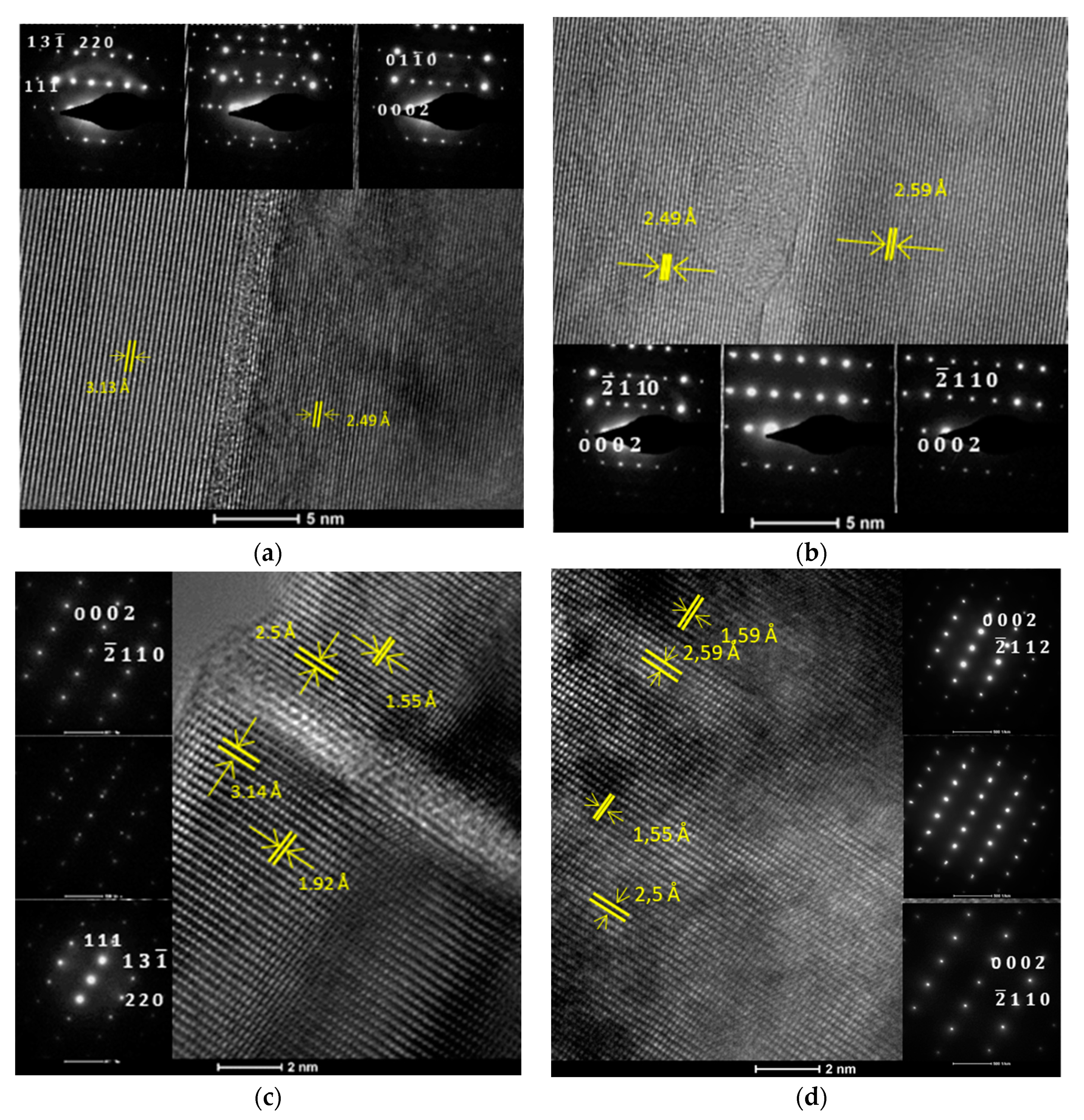
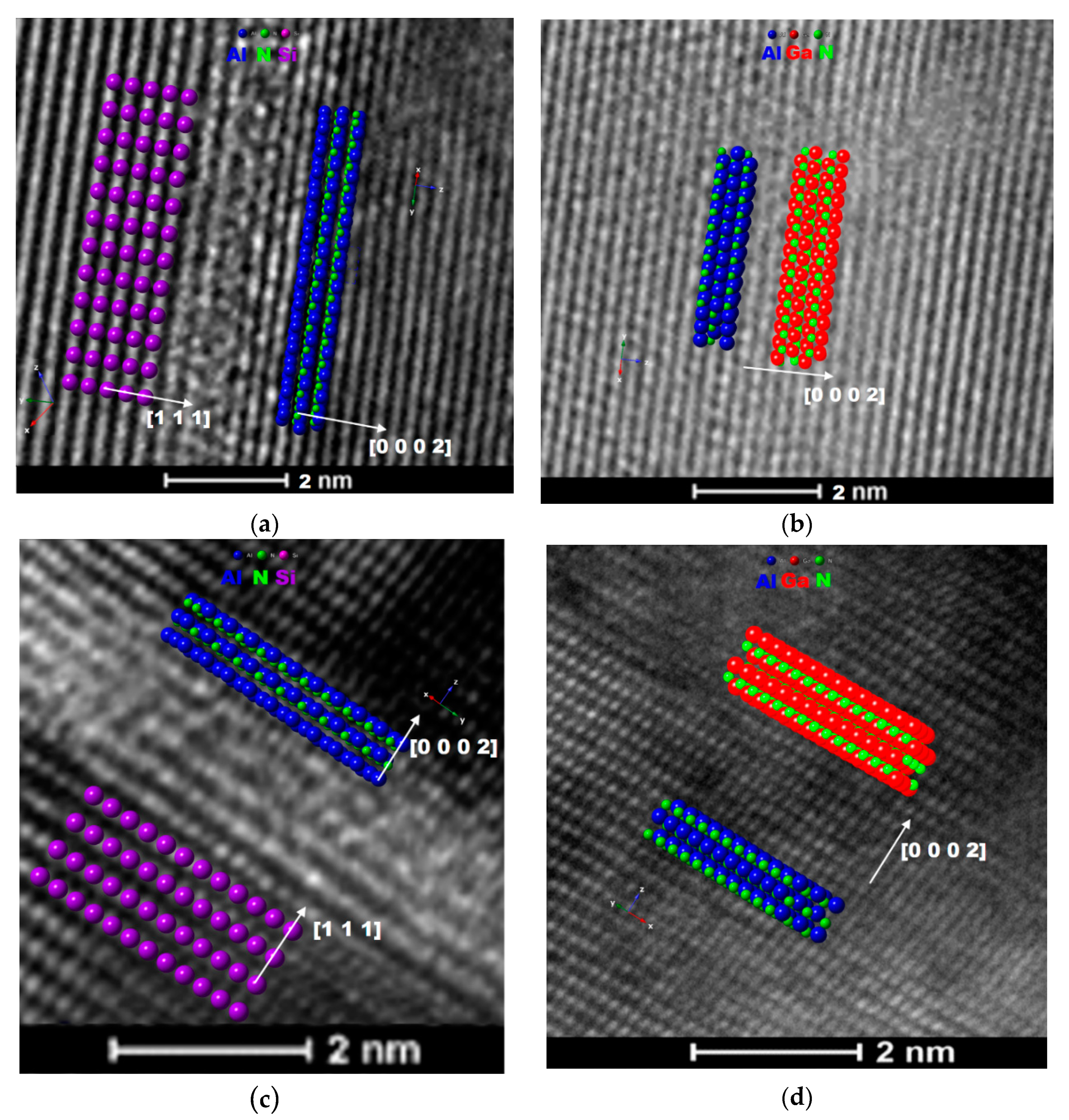
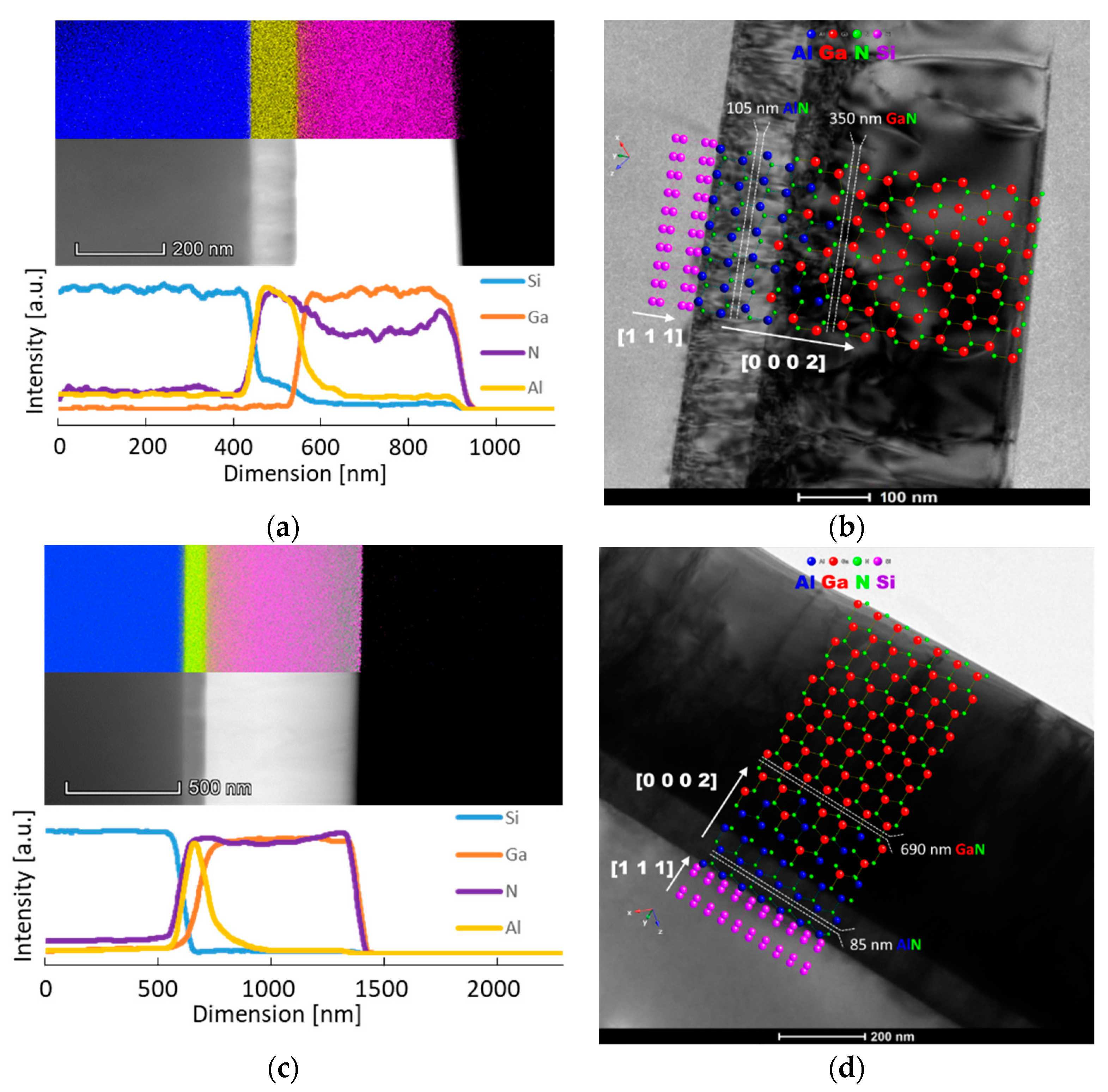
3.1.1. TEM
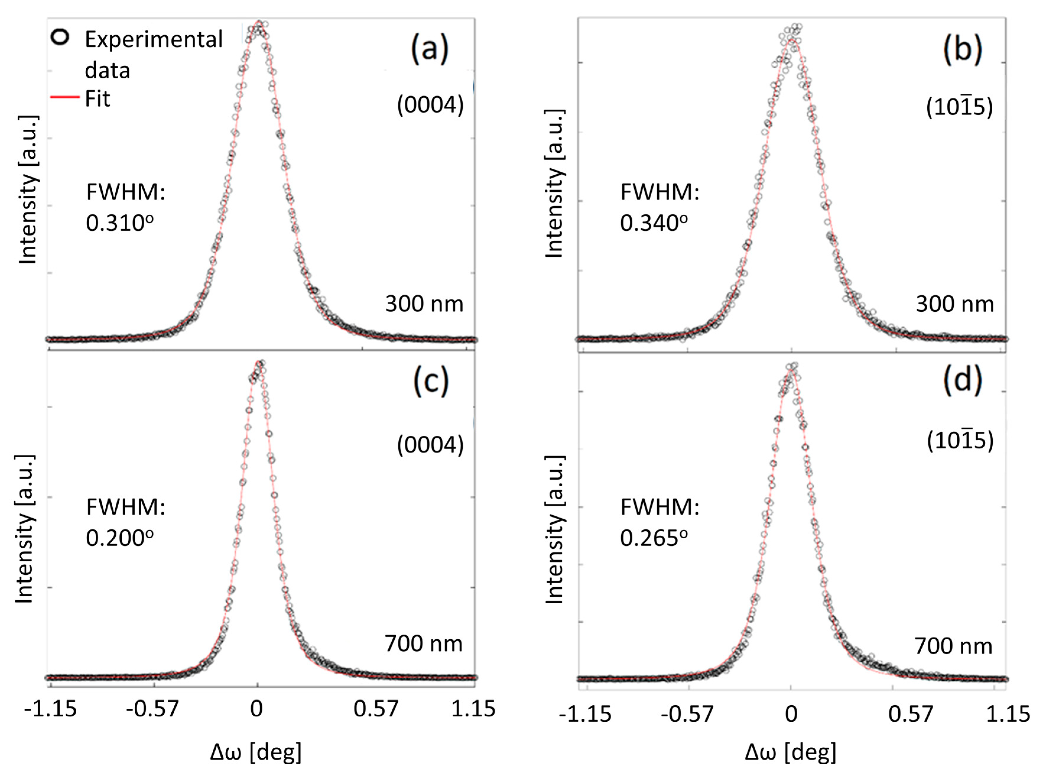
3.1.2. XRD
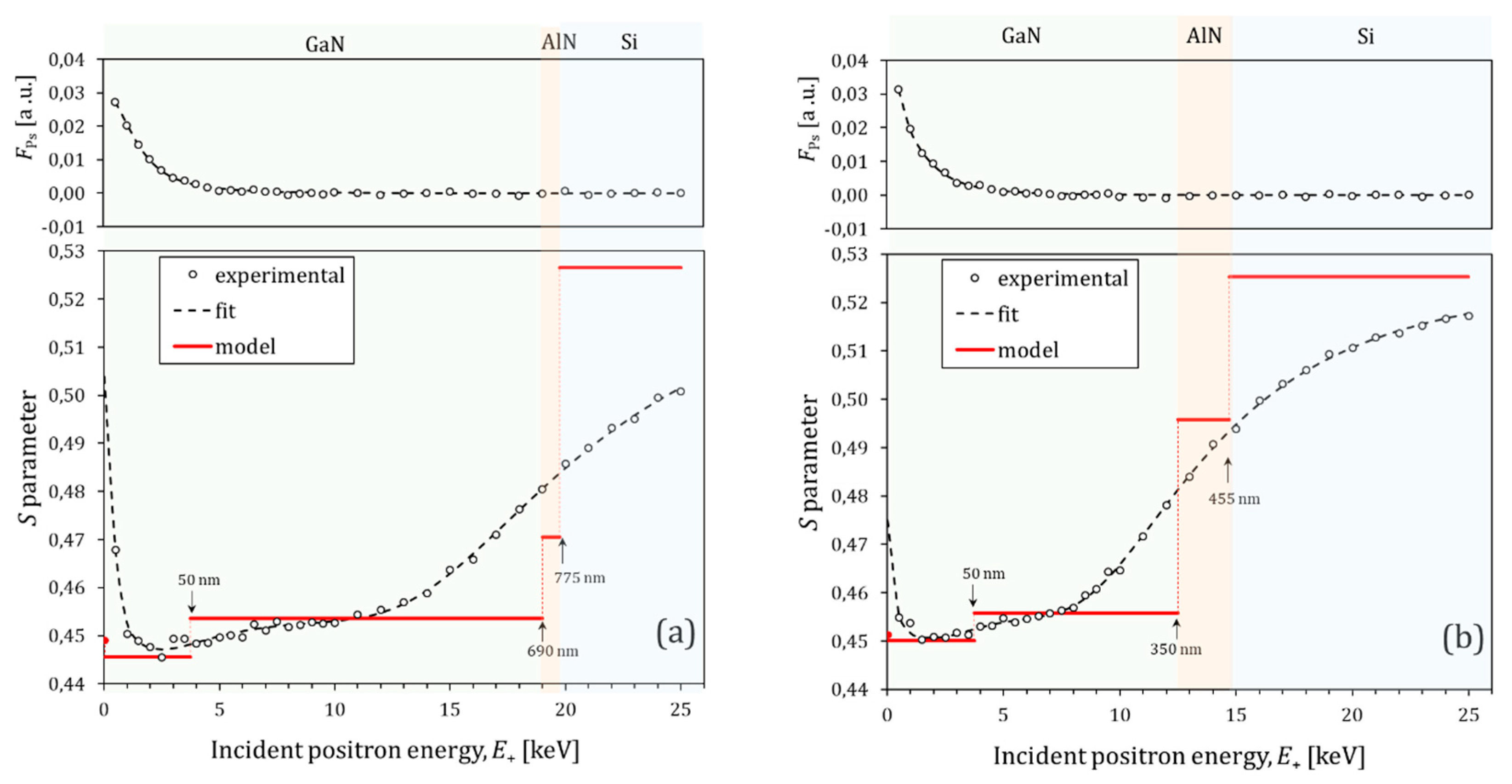
3.2. Positron Implantation Profile
4. Conclusions
Author Contributions
Funding
Acknowledgments
Conflicts of Interest
References
- Tsai, Y.L.; Lai, K.Y.; Lee, M.J.; Liao, Y.K.; Ooi, B.S.; Kuo, H.C.; He, J.H. Photon management of GaN-based optoelectronic devices via nanoscaled phenomena. Prog. Quantum Electron. 2016, 49, 1–25. [Google Scholar] [CrossRef]
- Pampili, P.; Parbrook, P.J. Doping of III-nitride materials. Mater. Sci. Semicond. Process. 2017, 62, 180–191. [Google Scholar] [CrossRef]
- Kuech, T.F. III-V compound semiconductors: Growth and structures. Prog. Cryst. Growth Charact. Mater. 2016, 62, 352–370. [Google Scholar] [CrossRef]
- Meneghini, M.; Tajalli, A.; Moens, P.; Banerjee, A.; Zanoni, E.; Meneghesso, G. Trapping phenomena and degradation mechanisms in GaN-based power HEMTs. Mater. Sci. Semicond. Process. 2018, 78, 118–126. [Google Scholar] [CrossRef]
- Roccaforte, F.; Fiorenza, P.; Greco, G.; Nigro, R.L.; Giannazzo, F.; Iucolano, F.; Saggio, M. Emerging trends in wide band gap semiconductors (SiC and GaN) technology for power devices. Microelectron. Eng. 2018, 78, 118–126. [Google Scholar] [CrossRef]
- Flack, T.J.; Pushpakaran, B.N.; Bayne, S.B. GaN Technology for Power Electronic Applications: A Review. J. Electron. Mater. 2016, 45, 2673–2682. [Google Scholar] [CrossRef]
- Carey, B.J.; Ou, J.Z.; Clark, R.M.; Berean, K.J.; Zavabeti, A.; Chesman, A.S.; Russo, S.P.; Lau, D.W.; Xu, Z.Q.; Bao, Q.; et al. Wafer-scale two-dimensional semiconductors from printed oxide skin of liquid metals. Nat. Commun. 2017, 8, 14482. [Google Scholar] [CrossRef]
- Syed, N.; Zavabeti, A.; Messalea, K.A.; Della Gaspera, E.; Elbourne, A.; Jannat, A.; Mohiuddin, M.; Zhang, B.Y.; Zheng, G.; Wang, L.; et al. Wafer-Sized Ultrathin Gallium and Indium Nitride Nanosheets through the Ammonolysis of Liquid Metal Derived Oxides. J. Am. Chem. Soc. 2019, 141, 104–108. [Google Scholar] [CrossRef]
- Daeneke, T.; Khoshmanesh, K.; Mahmood, N.; De Castro, I.A.; Esrafilzadeh, D.; Barrow, S.J.; Dickey, M.D.; Kalantar-Zadeh, K. Liquid metals: Fundamentals and applications in chemistry. Chem. Soc. Rev. 2018, 47, 4073–4111. [Google Scholar] [CrossRef]
- Merrison, J.P.; Charlton, M.; Deutch, B.I.; Jorgensen, L.V. Field assisted positron moderation by surface charging of rare gas solids. J. Phys. Condens. Matter 1992, 4, L207–L212. [Google Scholar] [CrossRef]
- Hugenschmidt, C. Positrons in surface physics. Surf. Sci. Rep. 2016, 71, 547–594. [Google Scholar] [CrossRef]
- Beling, C.D.; Fung, S.; Ming, L.; Gong, M.; Panda, B.K. Theoretical search for possible high efficiency semiconductor based field assisted positron moderators. Appl. Surf. Sci. 1999, 149, 253–259. [Google Scholar] [CrossRef]
- Jørgensen, L.V.; Schut, H. GaN-a new material for positron moderation. Appl. Surf. Sci. 2008, 255, 231–233. [Google Scholar] [CrossRef]
- Kukushkin, S.A.; Osipov, A.V.; Bessolov, V.N.; Medvedev, B.K.; Nevolin, V.K.; Tcarik, K.A. Substrates for epitaxy of Gallium Nitride:new materials and techniques. Rev. Adv. Mater. Sci. 2008, 17, 1–32. [Google Scholar]
- Yam, F.K.; Low, L.L.; Oh, S.A.; Hassan, Z. Gallium nitride: An overview of structural defects. In Optoelectronics—Materials and Techniques; IntechOpen Limited: London, UK, 2011; pp. 99–136. [Google Scholar]
- Ambacher, O. Growth and applications of Group III-nitrides. J. Phys. D Appl. Phys. 1998, 31, 2653–2710. [Google Scholar] [CrossRef]
- Schneider, C.A.; Rasband, W.S.; Eliceiri, K.W. NIH Image to ImageJ: 25 years of image analysis. Nat. Methods 2012, 9, 671–675. [Google Scholar] [CrossRef]
- Palmer, D.C. CrystalMaker; Begbroke: Oxfordshire, UK, 2014. [Google Scholar]
- Kaganer, V.M.; Brandt, O.; Trampert, A.; Ploog, K.H. X-ray diffraction peak profiles from threading dislocations in GaN epitaxial films. Phys. Rev. B Condens. Matter Mater. Phys. 2005, 72, 045423. [Google Scholar] [CrossRef]
- Tuomisto, F.; Makkonen, I. Defect identification in semiconductors with positron annihilation: Experiment and theory. Rev. Mod. Phys. 2013, 85, 1583–1631. [Google Scholar] [CrossRef]
- Van Veen, A.; Schut, H.; de Vries, J.; Hakvoort, R.A.; Ijpma, M.R. Analysis of positron profiling data by means of “VEPFIT”. AIP Conf. Proc. 1991, 218, 171–198. [Google Scholar]
- Van Veen, A.; Schut, H.; Clement, M.; de Nijs, J.M.M.; Kruseman, A.; IJpma, M.R. VEPFIT applied to depth profiling problems. Appl. Surf. Sci. 1995, 85, 216–224. [Google Scholar] [CrossRef]
- Yu, H.; Ozturk, M.K.; Ozcelik, S.; Ozbay, E. A study of semi-insulating GaN grown on AlN buffer/sapphire substrate by metalorganic chemical vapor deposition. J. Cryst. Growth 2006, 293, 273–277. [Google Scholar]
- Lahreche, H.; Vennéguès, P.; Tottereau, O.; Laügt, M.; Lorenzini, P.; Leroux, M.; Beaumont, B.; Gibart, P. Optimisation of AlN and GaN growth by metalorganic vapour-phase epitaxy (MOVPE) on Si (1 1 1). J. Cryst. Growth 2000, 217, 13–25. [Google Scholar] [CrossRef]
- Mánuel, J.M.; Morales, F.M.; García, R.; Aidam, R.; Kirste, L.; Ambacher, O. Threading dislocation propagation in AlGaN/GaN based HEMT structures grown on Si (111) by plasma assisted molecular beam epitaxy. J. Cryst. Growth 2012, 357, 35–41. [Google Scholar] [CrossRef]
- Yamaguchi, M.; Yamamoto, A.; Tachikawa, M.; Itoh, Y.; Sugo, M. Defect reduction effects in GaAs on Si substrates by thermal annealing. Appl. Phys. Lett. 1988, 53, 2293–2295. [Google Scholar] [CrossRef]
- Bogusławski, P.; Rapcewicz, K.; Bernholc, J.J. Surface segregation and interface stability of AlN/GaN, GaN/InN, and AlN/InN {0001} epitaxial systems. Phys. Rev. B 2000, 61, 10820–10826. [Google Scholar] [CrossRef]
- Romanitan, C.; Gavrila, R.; Danila, M. Comparative study of threading dislocations in GaN epitaxial layers by nondestructive methods. Mater. Sci. Semicond. Process. 2017, 57, 32–38. [Google Scholar] [CrossRef]
- Zubiaga, A.; García, J.A.; Plazaola, F.; Tuomisto, F.; Zúñiga-Pérez, J.; Muñoz-Sanjosé, V. Positron annihilation spectroscopy for the determination of thickness and defect profile in thin semiconductor layers. Phys. Rev. B 2007, 75, 205–305. [Google Scholar] [CrossRef]
- Schultz, P.J.; Tandberg, E.; Lynn, K.G.; Nielsen, B.; Jackman, T.E.; Denhoff, M.W.; Aers, G.C. Defects and Impurities at the Si/Si(100) Interface Studied with Monoenergetic Positrons. Phys. Rev. Lett. 1988, 61, 187–190. [Google Scholar] [CrossRef]
- Jean, Y.C.; Mallon, P.E.; Schrader, D.M. Principles and Applications of Positron and Positronium Chemistry; World Scientific Publishing Co.Pte.Ltd.: Singapore, 2003. [Google Scholar]
- Van Petegem, S.; Dauwe, C.; Van Hoecke, T.; De Baerdemaeker, J.; Segers, D. Diffusion length of positrons and positronium investigated using a positron beam with longitudinal geometry. Phys. Rev. B Condens. Matter Mater. Phys. 2004, 70, 115410. [Google Scholar] [CrossRef]
- Uedono, A.; Ishibashi, S.; Tenjinbayashi, K.; Tsutsui, T.; Nakahara, K.; Takamizu, D.; Chichibu, S.F. Defect characterization in Mg-doped GaN studied using a monoenergetic positron beam. J. Appl. Phys. 2012, 111, 014508. [Google Scholar] [CrossRef]
- Krause-Rehberg, R.; Leipner, H.S. Positron Annihilation in Semiconductors—Defect Studies; Springer-Verlag: Berlin/Heidelberg, Germany, 1999. [Google Scholar]
- Saleh, A.S.; Elhasi, A.M. Investigation of Positron Annihilation Diffusion Length in Gallium Nitride. Am. J. Mod. Phys. 2014, 3, 24–28. [Google Scholar] [CrossRef][Green Version]
- Pi, X.D.; Coleman, P.G.; Tseng, C.L.; Burrows, C.P.; Yavich, B.; Wang, W.N. Defects in GaN films studied by positron annihilation spectroscopy. J. Phys. Condens. Matter 2002, 14, L243–L248. [Google Scholar] [CrossRef]
- Puska, M.J.; Lanki, P.; Nieminen, R.M. Positron affinities for elemental metals. J. Phys. Condens. Matter 1999, 1, 6081–6094. [Google Scholar] [CrossRef]
- Makkonen, I.; Snicker, A.; Puska, M.J.; Mäki, J.M.; Tuomisto, F. Positrons as interface-sensitive probes of polar semiconductor heterostructures. Phys. Rev. B Condens. Matter Mater. Phys. 2010, 82, 041307. [Google Scholar] [CrossRef]
- Hu, Y.F.; Shan, Y.Y.; Beling, C.D.; Fung, S.; Xie, M.H.; Cheung, S.H.; Tu, J.; Brauer, G.; Anwand, W.; Tong, D.S. GaN Thin Films on SiC Substrates Studied Using Variable Energy Positron Annihilation Spectroscopy. In Materials Science Forum; Trans Tech Publications Ltd.: Zurich-Uetikon, Switzerland, 2001; Volume 363, pp. 478–480. [Google Scholar]


| Sample | [cm−2] | [cm−2] | [cm−2] | rd [nm] | Le [nm] | Ls [nm] |
|---|---|---|---|---|---|---|
| GaN300/Si | 4.19 × 10¹¹ | 1.85 × 10¹⁰ | 4.37 × 10¹¹ | 15 | 27 | 107 |
| GaN700/Si | 2.24 × 10¹¹ | 1.35 × 10¹⁰ | 2.35 × 10¹¹ | 21 | 41 | 220 |
| Sample | GaN300/Si χ2 = 1.15 | GaN700/Si χ2 = 1.73 | |||||
|---|---|---|---|---|---|---|---|
| Layer | Leff [nm] | S | d [nm] | Leff [nm] | S | d [nm] | |
| GaN | Sublayer | ||||||
| GaN1 | 14.3 ± 0.5 | 0.4501 ± 0.0006 | 50 | 13.1 ± 0.4 | 0.4456 ± 0.0004 | 50 | |
| GaN2 | 22 ± 6 | 0.4558 ± 0.0004 | 300 | 43 ± 6 | 0.4536 ± 0.0003 | 640 | |
| AlN | 26 ± 10 | 0.4957 ± 0.0019 | 105 | 4 ± 33 | 0.4707 ± 0.0032 | 85 | |
| Si | 245 | 0.5254 ± 0.0005 | - | 245 | 0.5264 ± 0.0011 | - | |
© 2020 by the authors. Licensee MDPI, Basel, Switzerland. This article is an open access article distributed under the terms and conditions of the Creative Commons Attribution (CC BY) license (http://creativecommons.org/licenses/by/4.0/).
Share and Cite
Ene, V.L.; Dinescu, D.; Djourelov, N.; Zai, I.; Vasile, B.S.; Serban, A.B.; Leca, V.; Andronescu, E. Defect Structure Determination of GaN Films in GaN/AlN/Si Heterostructures by HR-TEM, XRD, and Slow Positrons Experiments. Nanomaterials 2020, 10, 197. https://doi.org/10.3390/nano10020197
Ene VL, Dinescu D, Djourelov N, Zai I, Vasile BS, Serban AB, Leca V, Andronescu E. Defect Structure Determination of GaN Films in GaN/AlN/Si Heterostructures by HR-TEM, XRD, and Slow Positrons Experiments. Nanomaterials. 2020; 10(2):197. https://doi.org/10.3390/nano10020197
Chicago/Turabian StyleEne, Vladimir Lucian, Doru Dinescu, Nikolay Djourelov, Iulia Zai, Bogdan Stefan Vasile, Andreea Bianca Serban, Victor Leca, and Ecaterina Andronescu. 2020. "Defect Structure Determination of GaN Films in GaN/AlN/Si Heterostructures by HR-TEM, XRD, and Slow Positrons Experiments" Nanomaterials 10, no. 2: 197. https://doi.org/10.3390/nano10020197
APA StyleEne, V. L., Dinescu, D., Djourelov, N., Zai, I., Vasile, B. S., Serban, A. B., Leca, V., & Andronescu, E. (2020). Defect Structure Determination of GaN Films in GaN/AlN/Si Heterostructures by HR-TEM, XRD, and Slow Positrons Experiments. Nanomaterials, 10(2), 197. https://doi.org/10.3390/nano10020197