1. Introduction
The huge amount of new data generated every day has caused the need to search for new systems to store all this information in the smallest possible areas. S. Parkin proposed a new storage device called racetrack memory, in which magnetic domains are used to store the information in ferromagnetic stripes along its length [
1]. The magnetic domains would act like bits, separated by domain walls (DWs). In this novel system, the DWs are pinned at artificial defects created along the stripe, and the depinning is achieved by the application of spin-polarized current pulses [
2]. These pulses initiate the DWs movement, transporting the bits along the stripe reaching the read/write heads, increasing the speed of reading/writing data. In particular, 3D racetrack memories, made of arrays of vertically aligned nanowires, allow us to greatly increase the information density stored on a device.
The artificial defects used to pin the DWs are usually physical constraints placed at regular intervals throughout the magnetic stripe [
3,
4,
5,
6], and the distance between them allows us to control the bit size. However, despite the significant advantages of racetrack memories, like the increment in the information density or the high reading speed, this potential new storage device still has some limitations that prevent its implementation. Two of the main challenges that are under study are the need to avoid the Walker breakdown to increase the DW velocity [
7,
8], and the unwanted local Joule heating created at the notches when applying a current pulse through the wire to move the information pattern [
9,
10].
The first problem can be solved using cylindrical nanofibers instead of rectangular stripes, where it has been proven that the Walker breakdown limitation disappears [
7]. In addition to that, the use of nanofibers presents important advantages in comparison with the stripes: they can be fabricated in arrays by low-cost and high-yield electroplating methods (increasing the storage density), their geometry is easily tuned during the growing process and it is possible to grow segments of different materials along the wire [
11,
12,
13,
14].
On the other hand, by using nanofibers instead of stripes it is also possible to solve the second problem mentioned before: the possibility of manufacturing segments with different materials allows the creation of chemical rather than physical constraints [
15,
16,
17,
18,
19]. Chemical constraints consist of sections within the nanowire where the chemical composition changes with respect to the rest of the sample. If one segment of non-magnetic material is grown in the middle of two magnetic segments, the DW can be pinned at this constraint [
20,
21]. Its use avoids the presence of physical constraints, so the geometry does not change along the wire and the undesired overheating is eliminated. Many reports can be found on the fabrication of ordered arrays of vertically aligned cylindrical magnetic nanowires with chemical constraints along the wire’s length, such as Ni/Au [
22], Ni/Cu [
14], Ni
20Fe
80/Ni
70Fe
30 [
16], Co/Au [
17], Co/Cu [
11], Fe/Cu [
23], FeCoCu/Cu [
24] and FeGa/Cu [
25]. The morphology, chemical composition homogeneity, crystallographic structure and magnetic properties have also been thoroughly studied by scanning and transmission electron microscopy, electron energy loss spectroscopy, electron holography [
11], X-ray magnetic circular dichroism photoemission electron microscopy [
16,
19], magnetic force microscopy [
15], and bright-field transmission electron microscopy and Lorentz microscopy [
18]. Recent works have also proven the viability of such cylindrical magnetic nanowires with chemical constrains as key elements for magnetic recording, where pinning of the magnetic domain walls was confirmed at the constrains, and depinning accomplished by applying external magnetic fields [
16,
19].
Considering the easy tuning of racetrack nanowires during the electrodeposition process together with the use of chemical constraints, a novel 3D memory configuration is proposed in this work. The possibility to modify each segment in an individual way allows the creation of functional segments. Therefore, in this work we propose the integration of a writing section along the nanowire to replace the external writing heads. The creation of two different functional sections (writing and storage) along the same track provides a simpler way to write and store information in a high-density storage memory device. The main idea is to create a writing section made of two magnetic segments with different coercive fields, isolated from the storage section by a non-magnetic chemical constraint. By using a writing section that has one segment with a lower coercive field than the rest of the racetrack device allows us to switch its magnetization in an independent and easy way by applying a small external magnetic field. The information written in this first section can then be recorded into the racetrack memory wire by applying a spin-polarized current through the device, allowing us to push (and write) a new bit into the storage section of the track.
This work presents an in-depth study of the viability of this system as a 3D racetrack memory device using micromagnetic simulations. First, we demonstrate the viability of the writing section by simulating three different approaches to modify the coercivity of one segment: (i) physical (tuning the diameter), (ii) chemical (changing the chemical composition) and (iii) structural (adjusting the magnetocrystalline anisotropy). Once the bit has been successfully written using a magnetic field, we demonstrate the recording of the bit into the storage section by applying a spin-polarized current pulse through the nanowire. The use of a spin-current allowed the movement of all the DWs pinned at the chemical constraints along the track towards the adjacent pinning site, proofing the successful recording of the newly written bit without affecting the previously stored information. Finally, we analyze arrays of 3 and 7 nanowires to investigate the effect of neighboring magnetic wires in the bit movement of the central track. Our results show successful writing and storage processes even inside an array of nanowires, opening the possibility to use this system in a 3D racetrack memory device fabricated by industrially scalable methods.
2. Numerical Methods
Magnetic simulations were performed using the Object Oriented Micro-Magnetic Framework (OOMMF) project to solve the Landau-Lifshitz-Gilbert (LLG) equation [
26]. The LLG equation in the case where the current is aligned with the wire axis is given by [
27]:
In this equation,
γ, α,
,
t, and
correspond to the gyromagnetic ratio, Gilbert damping parameter, effective magnetic field, time, operator nabla and unit vector of the magnetization, respectively. The velocity
u is defined as:
where
J,
P,
g,
,
e and
, are the current density, the spin polarization rate, the g-factor of the electron, the Bohr magneton, the electron charge and the saturation magnetization, respectively. In this work, the current was simulated as pulses, and the external magnetic field was simulated as DC. Both of them were applied along the
x-axis, which corresponds to the long axis of the nanowires.
Individual and arrays of multi-segmented cylindrical nanowires composed of several magnetic segments (Ni or Co) separated by non-magnetic thin layers, were simulated. The Ni segments consist of pure Ni with an exchange constant of 9 × 10–12 J/m, a saturation magnetization of 490 × 103 A/m and no magnetocrystalline anisotropy. On the other hand, the Co segments have an exchange constant of 30 × 10−12 J/m and a saturation magnetization of 1400 × 103 A/m. Their magnetocrystalline anisotropy constant varies from zero, for the “Co without anisotropy” segments, to 5.7 × 10³ J/m3, if the segment is considered as “Co with anisotropy” (corresponding to Co nanowires with an hexagonal close-packed (hcp) crystallographic structure where the magnetocrystalline anisotropy axis is lying along the nanowire’s length). The non-magnetic segments were simulated without saturation magnetization nor exchange constant and will be referred to as Au segments.
The diameter of the nanowires was set to 40 nm, while the length of individual segments changed from 200 nm (for the Ni and Co segments) to 20 nm (for the non-magnetic chemical constraints). A cubic mesh with a unit cell size lower than the Ni and Co exchange lengths (
lex = 7.72 nm and
lex = 4.94 nm, respectively [
26]) is necessary, so a unit cell size of 4 nm was used in all simulations.
3. Results and Discussion
The two main challenges of a racetrack memory are the writing process and the bit movement. In this work, we simulate a novel model of a 3D racetrack memory where the use of functional segments eases to write and store information in a single cylindrical nanowire. This research has been performed through the analysis of three different stages: (1) the writing step, (2) the storage process (bit movement), and (3) the effect of neighboring nanowires during the DW movement in a single racetrack. The writing process has been performed by the application of an external magnetic field, and the bit movement has been achieved through a spin-polarized current pulse. Each process will be explained in detail in the following sections.
3.1. Writing Process
The writing process can be defined as the stage where one new bit is recorded. From a magnetic point of view, it means that the system should be able to inverse the magnetization of one segment of the nanowire in this stage, maintaining invariable the magnetization of the other segments.
In the proposed model, the memory recording is performed by the application of a magnetic field. The change in magnetization in only one segment of the entire nanowire is solely achieved when it presents any difference from the rest of the segments that reduces its coercive field. This difference can be physical, chemical, or structural:
Physical: By modifying the nanowire’s diameter one can easily tune its coercivity [
28,
29]. A segment with a larger diameter than the rest of the nanowire reverses its magnetization at lower applied magnetic fields (smaller coercivity). This modification can be easily scaled-up by adjusting the anodization conditions during template fabrication [
13]. For example, Salem et al. reported the fabrication of cylindrical Ni
80Fe
20 nanowires with modulated diameters by enlarging the pore diameter in a chemical bath prior to the final anodization process [
30]. On the other hand, Méndez et al. combined electrochemical anodization, atomic layer deposition and pore widening steps to fabricate diameter-modulated FeNi nanowires with sharp transition regions between the two segments of different diameters [
28].
Chemical: The deposition of two elements with different coercive fields (e.g., Ni and Co [
31,
32]) eases the creation of a writing segment without the need of modifying the initial template. Their fabrication follows a simple multi-step electroplating process with varying electrolyte compositions, as previously described elsewhere [
15,
18,
33].
Structural: By tuning the deposition parameters one can modify the crystallographic structure of the deposits, which, for elements with high magnetocrystalline anisotropy along the wire axis, will vary the coercive field. For example, the modification of the electrolyte pH during Co deposition can modify its structure from a face centered-cubic (fcc) one (with low magnetocrystalline anisotropy) into a hcp one (with high magnetocrystalline anisotropy) [
34,
35]. Other reports have also proved the fine-tuning of the crystallographic structures of Co nanowires by a pulsed-controlled electrochemical growth [
36,
37,
38]. In particular, Montazer et al. reported enhanced coercivities for large-diameter Co nanowires by adjusting the crystallographic structure of the deposits [
36].
The applied magnetic field used to switch the distinctive segment should be high enough to reverse its magnetization but small enough to avoid the inversion of magnetization in the other segments. To study all the potential differences mentioned before, the switching field of each possible segment has been estimated by simulating a single nanowire with four isolated magnetic segments: one of Ni with a larger diameter (80 nm instead of 40 nm), two with the same diameter but different elements (Ni and Co with negligible magnetocrystalline anisotropies and 40 nm in diameter); and a Co segment with an hcp crystallographic structure that induced a magnetocrystalline anisotropy along the wire’s length. To avoid the propagation of the magnetic domains from one segment to the adjacent one, non-magnetic Au segments of 150 nm were intercalated between the magnetic ones.
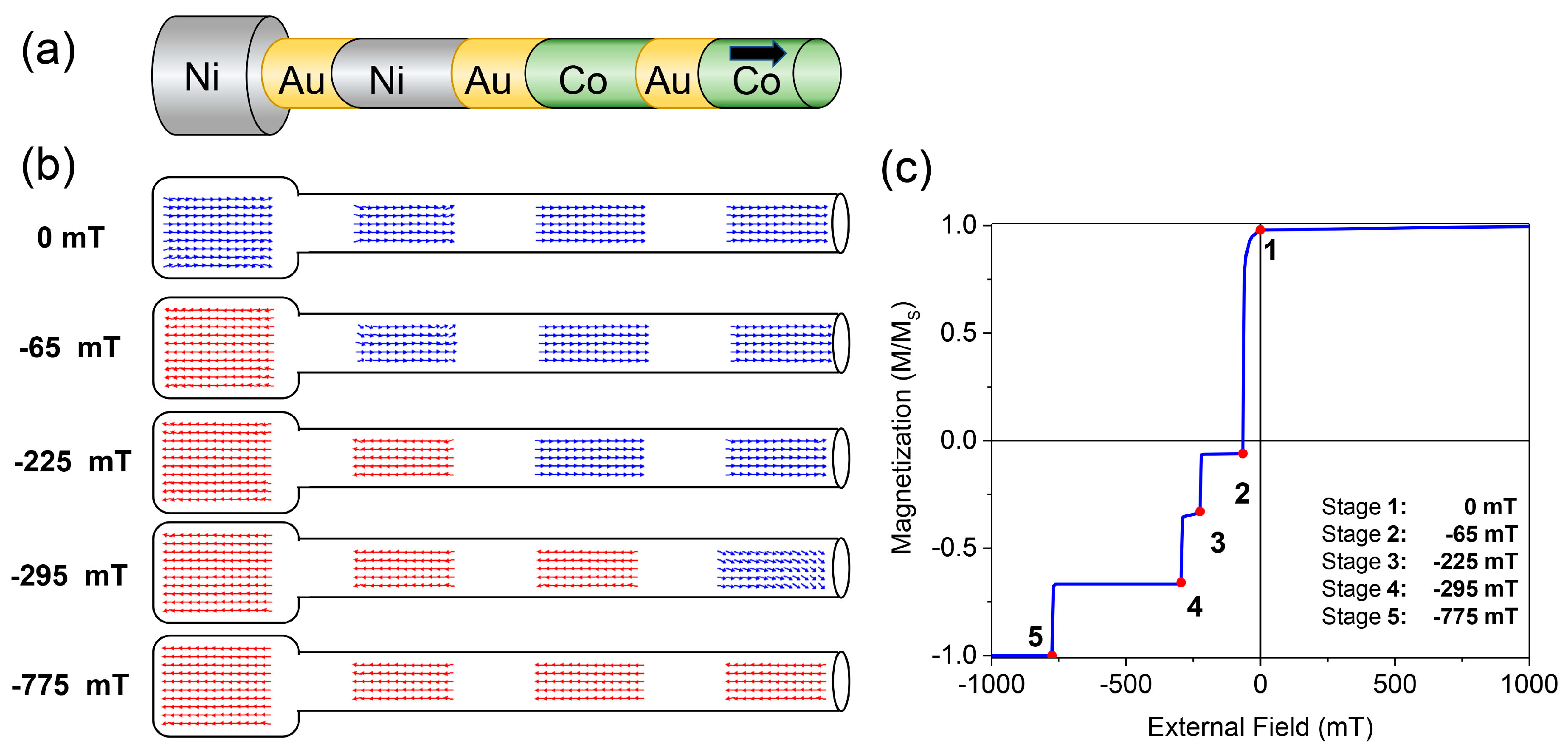
Figure 1a shows a representation of the simulated nanowire.
The demagnetization process of the different segments is schematically represented in
Figure 1b, where each stage corresponds to one drop in the hysteresis loop of the nanowire (
Figure 1c). As can be observed in
Figure 1b,c, all the segments maintain their magnetization in the remanence stage (0 mT), indicating that they could be used to store information, which is essential in a racetrack memory device. When a negative magnetic field is applied, the first segment that inverses its magnetization, i.e., the segment with the lowest coercive field (
Hc), is the one with a larger diameter (
Hc = 65 mT). As the external field increases (towards negative values), the next segment inversing its magnetization is the Ni-segment with a diameter of 40 nm. The difference in the exchange stiffness constant between Ni (9 × 10
−12 J/m) and Co (30 × 10
−12 J/m) causes the demagnetization of the Ni-segment at a lower field than in the case of the Co-segment. However, since both segments present the same diameter and zero magnetocrystalline anisotropy constant, the difference between their coercive fields is less than 100 mT (225 vs. 295 mT). The last segment that inverses its magnetization is the Co-segment with a large magnetocrystalline anisotropy constant (along the wire’s length), exhibiting a coercive field of 775 mT (
Figure 1c).
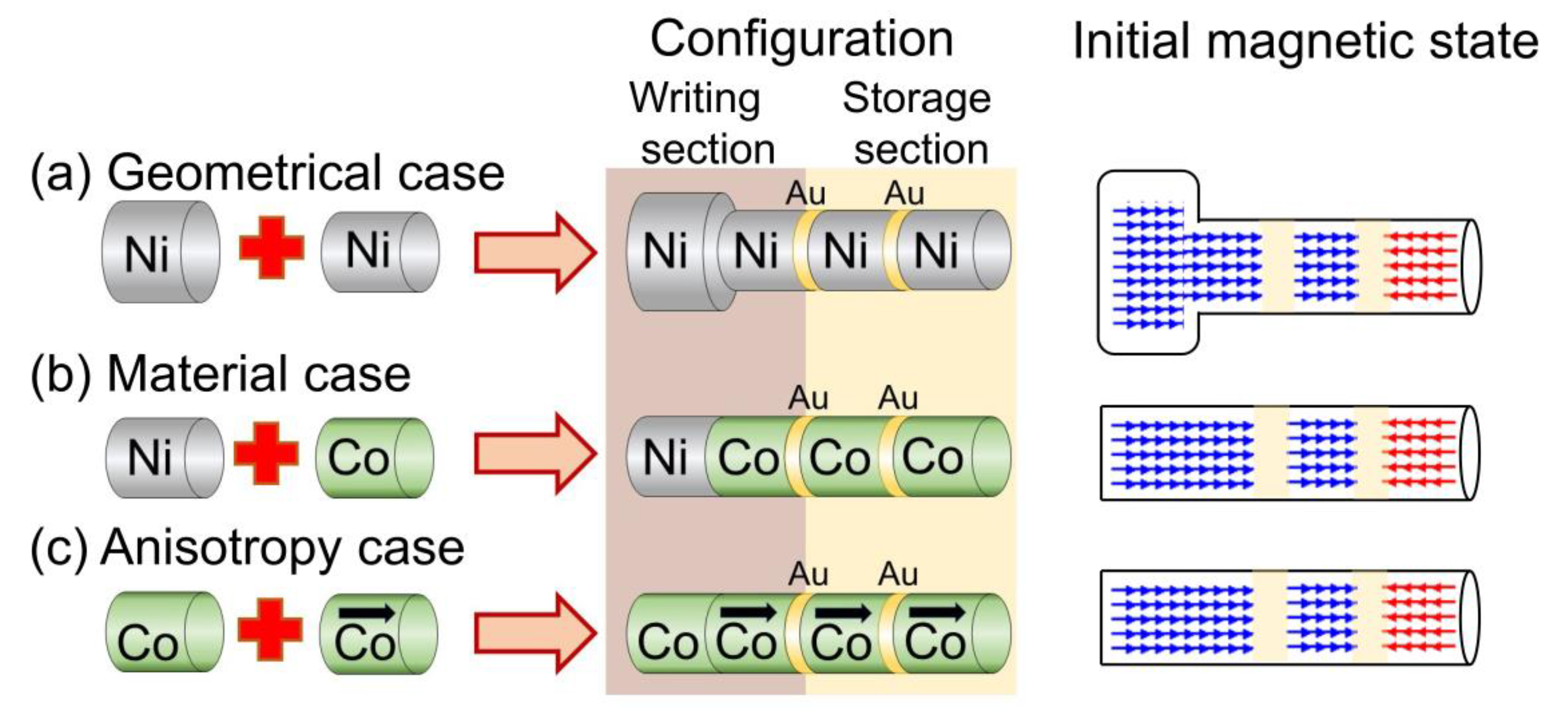
As explained before, the combination of segments with different coercivities would ease the magnetic modification of selective sections, maintaining invariant the other ones. The main idea is thus to create a writing section along the wire composed of two magnetic segments with different coercivities: a soft (low coercivity) magnetic segment that is different from the rest of the wire, and a harder (higher coercivity) magnetic segment, equal to the rest of the bit-storage segments. By being adjacent to each other, the reversal of the soft segment would induce the switching of the harder segment at a lower applied field than its coercivity. This first part of the wire (writing section), would then be separated from the rest of the wire (storage section) by a thin non-magnetic layer (chemical constraint), so it should show a lower coercive field than the rest of the nanowire. Based on the results shown in
Figure 1, three different possibilities for a racetrack memory are proposed (
Figure 2):
Geometrical case: The diameter of the soft magnetic segment is bigger. In this case, all the magnetic segments are made of the same element, Ni.
Material case: The first segment is made of Ni (Hc = 225 mT), while the rest of the magnetic segments are made of Co (Hc = 295 mT).
Anisotropy case: All the magnetic segments are made of Co, but the first magnetic segment is the only one with no magnetocrystalline anisotropy.
The lowest magnetic field that can be applied to switch the magnetization of the writing section in each case will be determined by the coercive field of the soft-segment. At the same time, the applied magnetic field cannot be higher than the coercive field of the hard-segments, since it would clean all the bits recorded in the nanowire.
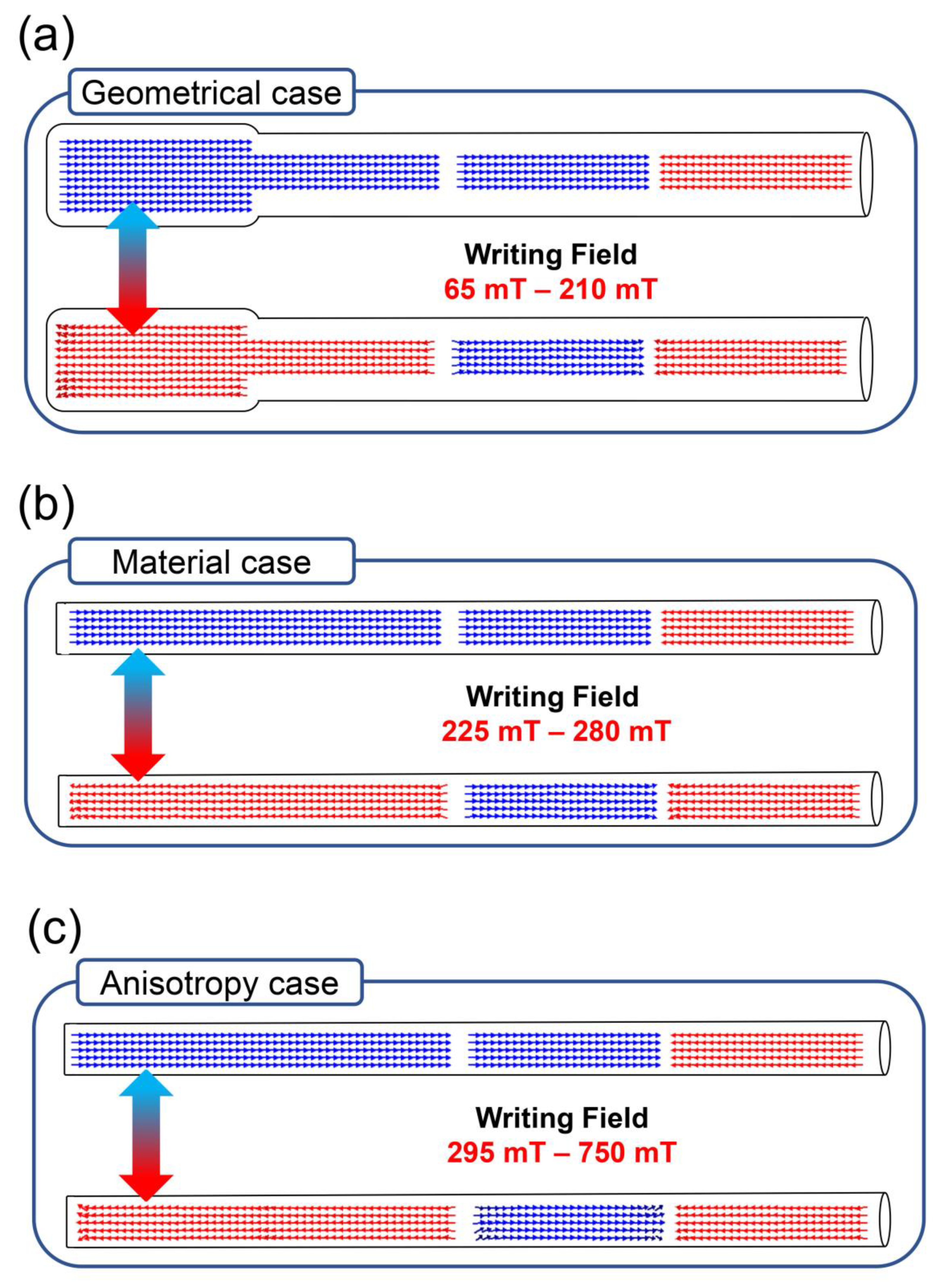
Figure 3 shows the range of “writing fields” that can be used in each case.
The three nanowires simulated can successfully reverse the magnetization of the writing section when applying a magnetic field in the range of 65–210 mT (geometrical case), 225–280 mT (material case) and 295–750 mT (anisotropy case) and maintaining invariant the magnetization of the rest of the nanowire. Independently of the success of the writing process, it can be observed that the highest magnetic field that can be applied to switch the magnetization in the writing section is slightly lower than the coercive field of the storage segments previously simulated (
Figure 1b,c). Since the non-magnetic Au segments in these nanowires are thinner than in the previous case (20 nm instead of 150 nm), the magnetic domains can propagate to adjacent segments if the applied field is too high. However, if the applied magnetic field is in the range shown in
Figure 3, the magnetic configuration of each segment cannot cause demagnetization of the adjacent one, so the information of the storage section stays invariant during the writing process. By maintaining invariant the length of the Au segments along the nanowire, the result presented here could be extrapolated to a nanowire with as many segments as desired, independently of the magnetic configuration of the system.
This result proves the effectiveness of the proposed model, where the construction of a single nanowire with two different types of segments together with the use of chemical constraints eases to write a bit in one segment without any variation in the rest of the track, by an external magnetic field. Once the bit has been written, the next step is its movement along the nanowire to record the information into the storage section of the racetrack. Based on previous experimental results, where a spin current was proven as a successful method to displace DWs in a stripe [
1,
2,
4,
39,
40,
41,
42,
43], the movement of the bits has been performed by the application of a current pulse.
3.2. Bit Movement
The bit movement is produced by applying a spin-polarized current pulse along the nanowire, which causes the propagation of the magnetic domains from a segment to the adjacent one. All the bit displacements should occur at the same time. A delay in the onset of one bit displacement could produce an overwriting in a storage segment before it is able to transmit its information to the following one. In order to avoid this delay, the transmissions must be produced between equal segments. For that reason, the scheme in
Figure 2 shows that the writing sections of the three cases are composed of two segments: one soft-segment with a lower coercive field (necessary to switch the magnetization) and, attached to it, a hard-segment with the same characteristics as the storage-segments. The latter is required for the magnetization propagation from the first segment to the following one to occur at the same time than the rest of the nanowire.
The propagation of the magnetic domains caused by the application of a spin-polarized current is only possible if the used current density is high enough to depin the DWs from the chemical constraints. This is directly related to the velocity u presented in the LLG equation (Equation 1). Therefore, the magnetic domains will only propagate to the adjacent segment if the vector u is high enough. Previously reported
u values are in the range of 100–600 m/s [
27,
44]. In this work, two different velocities have been used to displace the magnetic domains, attending whether the storage segments have magnetocrystalline anisotropy or not. A velocity of 100 m/s was used in the geometrical and material cases and 300 m/s in the anisotropy case, due to the extra difficulty observed in the propagation of magnetic domains in materials with magnetocrystalline anisotropy. However, although the velocity u in the first two cases is the same, it is important to remark that the vector u is directly related to the current density and inversely dependent on the saturation magnetization of the material (Equation 2). Therefore, the current density necessary to obtain the velocity mentioned before in an experimental work would be different in each case. The values used in this manuscript would correspond to an equivalent current density in the order of
J ≈ 10
11 A/m
2.
Figure 4 shows the magnetic domains propagation using the velocities mentioned before.
The results presented in
Figure 4 prove the success of the model proposed, achieving the propagation of the magnetic domains independently of the case exposed. The different velocity used in the geometrical, material and anisotropy cases explains the great disparity observed in the propagation time: while the anisotropy case only needs 1 ns to finish the propagation of the magnetic domain from one segment to the adjacent one, 10.3 and 11 ns are needed to observe the same propagation in the material and the geometrical cases, respectively. Despite the time needed or the velocity used, the DW formed inside each segment during the domain movement can be described in the three cases as a transversal like DW. This result is in good agreement with Castilla et al. [
20], where it is reported that the pinning of a DW in a chemical constraint (the Au segment in this case) transforms any kind of DW into a transversal DW, which is also observed in these simulations. The movement of the transversal DW under the application of a spin current has been studied by the animation of the storage process in the geometrical case, which is shown in
Supplementary information Video S1. The 3D animation shows a first stage where the transversal DW is formed and a second stage where it is propagated along the segment. These two stages can be well-differentiated by observing the rotation of the DW. During its formation, the DW shows a rotation around the segment, which disappears once the DW is stable and starts its linear propagation throughout the segment.
Direct comparison between
Figure 3 and
Figure 4 proves how the use of a 20 nm-thick Au layer to isolate the magnetic segments successfully manages to pin the domain wall at the chemical constraint and, at the same time, allows its depinning when a spin-current is applied through the nanowire.
The simulated starting magnetic configuration in this section was chosen with the purpose of being able to observe the DW propagation along the two storage sections at the same time. Nevertheless, since the initial magnetic configuration does not influence the onset of the DW movement, all the possible magnetic configurations would initiate the depinning process at the same time. In an up-scale process with tens of storage sections in a single nanowire, the expected behavior in this longer nanowire would be the same than that observed in
Figure 4.
Once the proposed model has been proved as an interesting option for a racetrack memory, the next step is to study its viability as a 3D storage device. For that, we will investigate the bit movement in a single nanowire inside an array of several nanowires, as magnetostatic interactions between neighboring elements are known to influence the magnetization reversal process [
45,
46,
47].
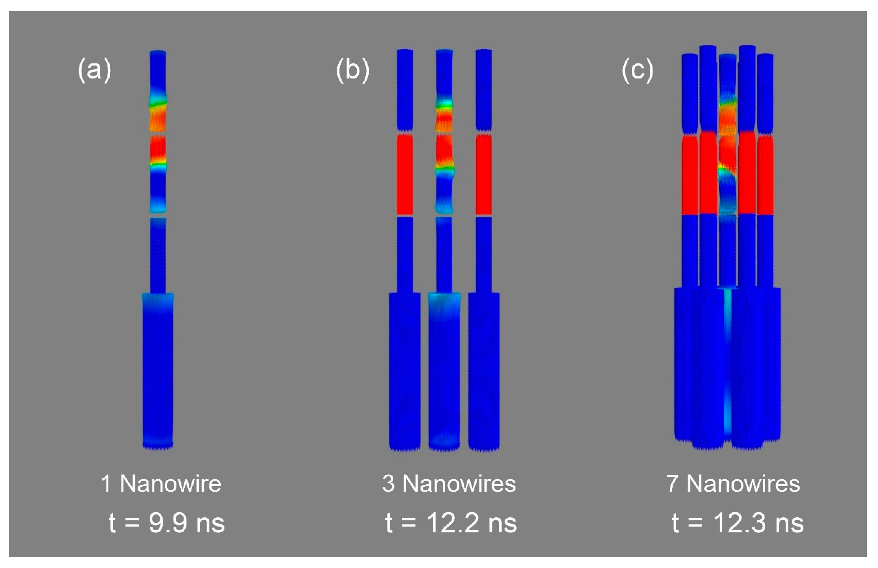
3.3. Arrays of Nanowires as 3D Racetrack Memories
Two different arrays with 3 and 7 nanowires (hexagonal array), respectively, have been simulated to investigate the effect of neighboring magnetic wires in the bit movement of the central wire. For simplicity, and given the similarity of results, in this section only the geometrical case has been considered.
As all the nanowires are identical, the writing-section of all of them will switch their magnetization under similar applied fields [
45]. The presence of neighboring wires will reduce the overall switching field but will still maintain a similar writing field range as displayed in
Figure 3. On the other hand, the bit movement of each nanowire should be performed individually, so it is necessary to investigate the possible influence of the neighboring nanowires when a spin current is applied to the central one. For that, the spins of the external nanowires were fixed during the simulation of the bit-movement in the central nanowire. 3D representations of the three different configurations compared in this section are plotted in
Figure 5. With the aim of comparing the bit movement under the same conditions, the velocity u in all cases has been set to 100 m/s. The center-to-center distance between the nanowires was set to 104 nm, based on previous experiments using nanoporous alumina templates [
47,
48].
Simulations show that magnetic domains can propagate from one segment to the adjacent one even when in an array with 3 or 7 nanowires, but a longer pulse time is needed. The presence of neighboring nanowires thus delays the bit movement.
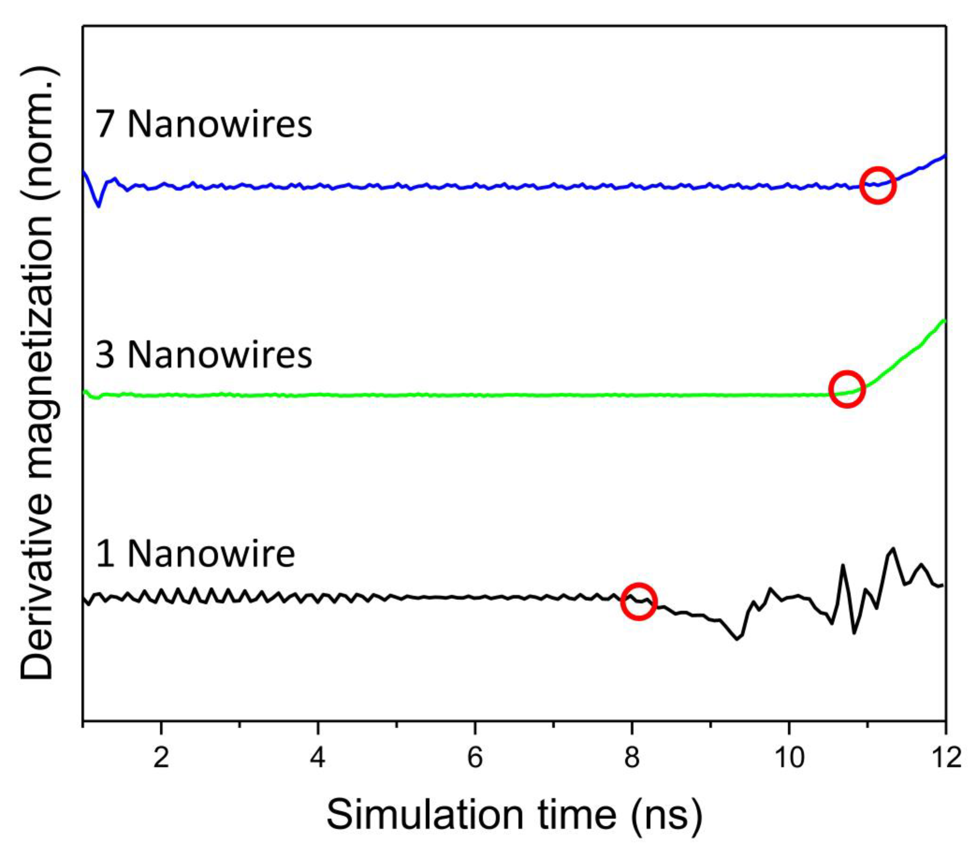
Figure 6 shows the derivate of the magnetization value along the wire (
Mx) for each case. It can be clearly seen how the onset of the bit movement increases from 8.1 to 10.8 ns in the case of 1 and 3 nanowires, respectively, and reaches 11.2 ns in an array of 7 nanowires. These results show a significant delay of almost 3 ns in the depinning of the DW when the central nanowire has others surrounding it, which is a critical difference that should be considered in the experimental development of a future 3D racetrack memory device. However, it can be observed that the number of nanowires around it only slightly modifies this onset (10.8 vs. 11.2 ns), so the density of nanowires in the array does not seem to be a key factor in the development of the 3D racetrack memory. As in the previous case where it was analyzed a single nanowire, the magnetic configuration of the surrounding nanowires does not introduce any modification in the depinning process.
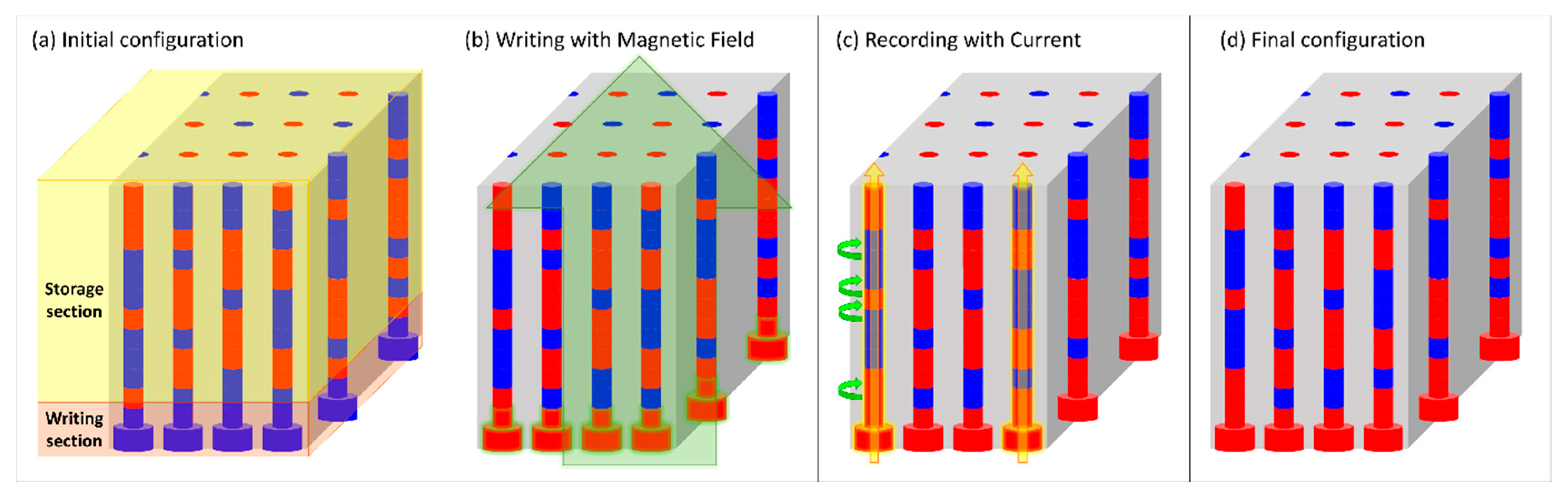
To conclude, we present in
Figure 7 a schematic representation of a 3D racetrack memory device based on the novel design proposed in this work. The device is composed of an array of vertically aligned cylindrical nanowires (racetracks). Each track is made of a storage section (capable of recording 11 bits of information) and a writing section (comprising an additional information bit and a lager diameter segment (soft-segment)). By applying a small external magnetic field, the magnetization of the writing section reverses while keeping the initial configuration of the storage section (no data is lost between
Figure 7a,b). To record the new information into the memory device, a spin-polarized current is applied to selected tracks (yellow arrows in
Figure 7c). From the experimental point-of-view, this could be performed following a nano-identation procedure described elsewhere [
49,
50] optimized through different automatic compilation frameworks [
51] or through reinforced learning [
52]. Although existing characterization techniques do not yet allow a fast access of individual tracks in a vertical array, this type of equipment is constantly being updated with innovative designs and functionalities, so these measurements may become feasible in the near future. Meanwhile, combinations of nano-lithographed patterns with atomic force microscopy nano-identation techniques would allow preliminary studies of the feasibility of such 3D nano-memory devices. At the end of the process, we were able to simultaneously record two bits of information into two different tracks (
Figure 7d).
Supplementary information Figure S1 shows an animated representation of the writing and storage processes in which several different bits are recorded at the same time.
4. Conclusions
In this work, a novel 3D racetrack memory configuration based on functional segments inside cylindrical nanowire arrays has been proposed. The integration of the writing and the storage sections inside the same track has been studied through micromagnetic simulations, proving the success of this novel configuration without the use of external writing heads.
The incorporation of the writing and the storage sections together has been made possible by growing two kinds of segments with different magnetic properties in a single nanowire. Micromagnetic simulations of cylindrical nanowires based on magnetic segments of Ni and Co have demonstrated the possibility to reduce the coercive field of one segment of the nanowire by different modifications: physical, chemical, or structural.
The ability to grown two kinds of magnetic segments with different coercivities has been used to build a writing section in the nanowire. This section has been made by the combination of a soft (low coercivity) magnetic segment with a harder (higher coercivity) magnetic segment, equal to the rest of the bit-storage segments (storage section). By being adjacent to each other, magnetic simulations have shown how the reversal of the soft segment can induce the switching of the harder segment at a lower applied field than its coercivity, writing the new bit. The use of a thin non-magnetic layer (chemical constraint) between the writing section and the rest of the wire (storage section) avoids the propagation of the magnetization reversal to the following segments; keeping the storage section invariant during the writing process and preserving the information stored in the rest of the nanowire.
While the bit recording process was performed under the application of an external magnetic field, the store of the new bit was achieved using spin-current pulses. Magnetic simulations have shown how the application of spin-current pulses causes the domain wall movement from one magnetic segment to the adjacent one, pushing the new bit into the following section of the wire and allowing its storage. The simulations have proven that the presence of chemical constraints along the nanowire stops the inversion of the magnetization during the writing process and, at the same time, allows the domain wall movement when a spin-polarized current pulse is applied.
Finally, we studied the effect of neighboring nanowires when a spin current is applied to the central nanowire, proving that it is also possible to write and store a bit in a nanowire inside an array. The neighboring nanowires cause a delay in the domain wall movement when a spin-current is applied, but their presence does not prevent the storage process.
These results suppose a breakthrough in the research of 3D racetrack memory configuration. While most of the studies are based on the research of rectangular stripes where it is not possible to grown functional sections, this work presents a novel configuration where it is possible to write and record bits in cylindrical nanowires. The use of nanowires instead of stripes enables the growth of thousands of wires in a single deposition, reducing the cost and increasing the information density of the memory.
Author Contributions
M.P.P. conceived the idea. J.R. performed the micromagnetic simulations with the help of M.P.P. Both authors analyzed and discussed the results. J.R. wrote the manuscript with the help of M.P.P. M.P.P. acquired funding and supervised the project. All authors have read and agreed to the published version of the manuscript.
Funding
This research was funded by FCT and COMPETE 2020 (FEDER) under projects POCI-01-0145-FEDER-028676 and UIDB/04968/2020, and by the Spanish Ministerio de Ciencia e Innovación under the project MAT2017-87072-C4-3-P.
Acknowledgments
The authors acknowledge financial support by the Portuguese Fundação para a Ciência e Tecnologia (FCT) and COMPETE 2020 (FEDER) under the projects POCI-01-0145-FEDER-028676 and UIDB/04968/2020, and by the Spanish Ministerio de Ciencia e Innovación under the project MAT2017-87072-C4-3-P.
Conflicts of Interest
The authors declare no conflict of interest. The founders had no role in the design of the study; in the collect ion, analyses, or interpretation of data; in the writing of the manuscript, or in the decision to publish the results.
References
- Parkin, S.S.P.; Hayashi, M.; Thomas, L. Magnetic domain-wall racetrack memory. Science 2008, 320, 190–194. [Google Scholar] [CrossRef] [PubMed]
- Hayashi, M.; Thomas, L.; Moriya, R.; Rettner, C.; Parkin, S.S.P. Current-controlled magnetic domain-wall nanowire shift register. Science 2008, 320, 209–211. [Google Scholar] [CrossRef] [PubMed]
- Muñoz, M.; Prieto, J.L. Suppression of the intrinsic stochastic pinning of domain walls in magnetic nanostripes. Nat. Commun. 2011, 2, 562. [Google Scholar] [CrossRef]
- Nguyen, V.D.; Torres, W.S.; Laczkowski, P.; Marty, A.; Jamet, M.; Beigné, C.; Notin, L.; Vila, L.; Attané, J.P. Elementary depinning processes of magnetic domain walls under fields and currents. Sci. Rep. 2014, 4, 6509. [Google Scholar] [CrossRef] [PubMed]
- Bran, C.; Berganza, E.; Palmero, E.M.; Fernandez-Roldan, J.A.; Del Real, R.P.; Aballe, L.; Foerster, M.; Asenjo, A.; Fraile Rodríguez, A.; Vazquez, M. Spin configuration of cylindrical bamboo-like magnetic nanowires. J. Mater. Chem. C 2016, 4, 978–984. [Google Scholar] [CrossRef]
- Iglesias-Freire, Ó.; Bran, C.; Berganza, E.; Mínguez-Bacho, I.; Magén, C.; Vázquez, M.; Asenjo, A. Spin configuration in isolated FeCoCu nanowires modulated in diameter. Nanotechnology 2015, 26, 395702. [Google Scholar] [CrossRef]
- Biziere, N.; Gatel, C.; Lassalle-Balier, R.; Clochard, M.C.; Wegrowe, J.E.; Snoeck, E. Imaging the fine structure of a magnetic domain wall in a Ni nanocylinder. Nano Lett. 2013, 13, 2053–2057. [Google Scholar] [CrossRef]
- Fernandez-Roldan, J.A.; Ivanov, Y.P.; Chubykalo-Fesenko, O. Micromagnetic modeling of magnetic domain walls and domains in cylindrical nanowires. In Magnetic Nano- and Microwires, 2nd ed.; Vazquez, M., Ed.; Elsevier: Cambridge, UK, 2020; pp. 403–426. [Google Scholar] [CrossRef]
- Ramos, E.; López, C.; Akerman, J.; Muñoz, M.; Prieto, J.L. Joule heating in ferromagnetic nanostripes with a notch. Phys. Rev. B 2015, 91, 214404. [Google Scholar] [CrossRef]
- Prieto, J.L.; Muñoz, M.; Raposo, V.; Martínez, E. Joule heating and its role in current-assisted domain wall depinning in nanostrips. In Magnetic Nano- and Microwires, 2nd ed.; Vazquez, M., Ed.; Elsevier: Cambridge, UK, 2020; pp. 325–360. [Google Scholar] [CrossRef]
- Reyes, D.; Biziere, N.; Warot-Fonrose, B.; Wade, T.; Gatel, C. Magnetic Configurations in Co/Cu Multilayered Nanowires: Evidence of Structural and Magnetic Interplay. Nano Lett. 2016, 16, 1230–1236. [Google Scholar] [CrossRef]
- Zhang, W.; Li, H.; Wang, H.; Yao, S. Effect of Nanowire Diameter and Period Number on Magnetic Properties and CPP-GMR of Ni-Fe/Cu/Co/Cu Multilayer Nanowire Arrays. J. Electrochem. Soc. 2014, 161, D176–D180. [Google Scholar] [CrossRef]
- Sousa, C.T.; Leitao, D.C.; Proenca, M.P.; Ventura, J.; Pereira, A.M.; Araujo, J.P. Nanoporous alumina as templates for multifunctional applications. Appl. Phys. Rev. 2014, 1, 031102. [Google Scholar] [CrossRef]
- Susano, M.; Proenca, M.P.; Moraes, S.; Sousa, C.T.; Arajo, J.P. Tuning the magnetic properties of multisegmented Ni/Cu electrodeposited nanowires with controllable Ni lengths. Nanotechnology 2016, 27, 335301. [Google Scholar] [CrossRef]
- Berganza, E.; Jaafar, M.; Bran, C.; Fernández-Roldán, J.A.; Chubykalo-Fesenko, O.; Vázquez, M.; Asenjo, A. Multisegmented Nanowires: A Step towards the Control of the Domain Wall Configuration. Sci. Rep. 2017, 7, 11576. [Google Scholar] [CrossRef]
- Ruiz-Gómez, S.; Foerster, M.; Aballe, L.; Proenca, M.P.; Lucas, I.; Prieto, J.L.; Mascaraque, A.; de la Figuera, J.; Quesada, A.; Pérez, L. Observation of a topologically protected state in a magnetic domain wall stabilized by a ferromagnetic chemical barrier. Sci. Rep. 2018, 8, 16695. [Google Scholar] [CrossRef] [PubMed]
- Bran, C.; Ivanov, Y.P.; Kosel, J.; Chubykalo-Fesenko, O.; Vazquez, M. Co/Au multisegmented nanowires: A 3D array of magnetostatically coupled nanopillars. Nanotechnology 2017, 28, 095709. [Google Scholar] [CrossRef] [PubMed]
- Ivanov, Y.P.; Chuvilin, A.; Lopatin, S.; Kosel, J. Modulated Magnetic Nanowires for Controlling Domain Wall Motion: Toward 3D Magnetic Memories. ACS Nano 2016, 10, 5326–5332. [Google Scholar] [CrossRef]
- Ruiz-Gómez, S.; Fernández-González, C.; Martínez, E.; Raposo, V.; Sorrentino, A.; Foerster, M.; Aballe, L.; Mascaraque, A.; Ferrer, S.; Pérez, L. Helical surface magnetization in nanowires: The role of chirality. Nanoscale 2020, 12, 17880–17885. [Google Scholar] [CrossRef]
- Castilla, D.; Maicas, M.; Prieto, J.L.; Proenca, M.P. Depinning process of magnetic domain walls in cylindrical nanowires with a chemical constraint. J. Phys. D. Appl. Phys. 2017, 50, 105001. [Google Scholar] [CrossRef]
- Bran, C.; Berganza, E.; Fernandez-Roldan, J.A.; Palmero, E.M.; Meier, J.; Calle, E.; Jaafar, M.; Foerster, M.; Aballe, L.; Fraile Rodriguez, A.; et al. Magnetization Ratchet in Cylindrical Nanowires. ACS Nano 2018, 12, 5932–5939. [Google Scholar] [CrossRef]
- Clime, L.; Zhao, S.Y.; Chen, P.; Normandin, F.; Roberge, H.; Veres, T. The interaction field in arrays of ferromagnetic barcode nanowires. Nanotechnology 2007, 18, 435709. [Google Scholar] [CrossRef]
- Moraes, S.; Navas, D.; Béron, F.; Proenca, M.P.; Pirota, K.R.; Sousa, C.T.; Araújo, J.P. The role of Cu length on the magnetic behaviour of Fe/Cu multi-segmented nanowires. Nanomaterials 2018, 8, 490. [Google Scholar] [CrossRef] [PubMed]
- Núñez, A.; Pérez, L.; Abuín, M.; Araujo, J.P.; Proenca, M.P. Magnetic behaviour of multisegmented FeCoCu/Cu electrodeposited nanowires. J. Phys. D. Appl. Phys. 2017, 50, 155003. [Google Scholar] [CrossRef]
- Reddy, S.M.; Park, J.J.; Na, S.M.; Maqableh, M.M.; Flatau, A.B.; Stadler, B.J.H. Electrochemical synthesis of magnetostrictive Fe-Ga/Cu multilayered nanowire arrays with tailored magnetic response. Adv. Funct. Mater. 2011, 21, 4677–4683. [Google Scholar] [CrossRef]
- Donahue, M.J.; Porter, D.G. OOMMF User’s Guide, Version 1.0, Interagency Report NISTIR 6376; Technical 427 Report; National Institute of Standards and Technology: Gaithersburg, MD, USA, 1999. Available online: https://math.nist.gov/oommf/ (accessed on 16 June 2020).
- Thiaville, A.; Nakatani, Y.; Miltat, J.; Suzuki, Y. Micromagnetic understanding of current-driven domain wall motion in patterned nanowires. Europhys. Lett. 2005, 69, 990–996. [Google Scholar] [CrossRef]
- Méndez, M.; Vega, V.; González, S.; Caballero-Flores, R.; García, J.; Prida, V.M. Effect of sharp diameter geometrical modulation on the magnetization reversal of bi-segmented feni nanowires. Nanomaterials 2018, 8, 595. [Google Scholar] [CrossRef]
- Palmero, E.M.; Méndez, M.; González, S.; Bran, C.; Vega, V.; Vázquez, M.; Prida, V.M. Stepwise magnetization reversal of geometrically tuned in diameter Ni and FeCo bi-segmented nanowire arrays. Nano Res. 2019, 12, 1547–1553. [Google Scholar] [CrossRef]
- Salem, M.S.; Sergelius, P.; Corona, R.M.; Escrig, J.; Görlitz, D.; Nielsch, K. Magnetic properties of cylindrical diameter modulated Ni 80Fe20 nanowires: Interaction and coercive fields. Nanoscale 2013, 5, 3941–3947. [Google Scholar] [CrossRef]
- Proenca, M.P.; Sousa, C.T.; Ventura, J.; Araujo, J.P.; Escrig, J.; Vazquez, M. Crossover between magnetic reversal modes in ordered ni and co nanotube arrays. Spin 2012, 2, 1250014. [Google Scholar] [CrossRef]
- García Fernández, J.; Vega Martínez, V.; Thomas, A.; de la Prida Pidal, V.M.; Nielsch, K. Two-step magnetization reversal FORC fingerprint of coupled bi-segmented Ni/Co magnetic nanowire arrays. Nanomaterials 2018, 8, 548. [Google Scholar] [CrossRef]
- Méndez, M.; González, S.; Vega, V.; Teixeira, J.M.; Hernando, B.; Luna, C.; Prida, V.M. Ni-Co alloy and multisegmented Ni/Co nanowire arrays modulated in composition: Structural characterization and magnetic properties. Crystals 2017, 7, 66. [Google Scholar] [CrossRef]
- Vivas, L.G.; Escrig, J.; Trabada, D.G.; Badini-Confalonieri, G.A.; Vázquez, M. Magnetic anisotropy in ordered textured Co nanowires. Appl. Phys. Lett. 2012, 100, 252405. [Google Scholar] [CrossRef]
- Ivanov, Y.P.; Trabada, D.G.; Chuvilin, A.; Kosel, J.; Chubykalo-Fesenko, O.; Vázquez, M. Crystallographically driven magnetic behaviour of arrays of monocrystalline Co nanowires. Nanotechnology 2014, 25, 475702. [Google Scholar] [CrossRef]
- Montazer, A.H.; Ramazani, A.; Kashi, M.A.; Zavašnik, J. Developing high coercivity in large diameter cobalt nanowire arrays. J. Phys. D Appl. Phys. 2016, 49, 445001. [Google Scholar] [CrossRef]
- Pirota, K.R.; Béron, F.; Zanchet, D.; Rocha, T.C.R.; Navas, D.; Torrejón, J.; Vazquez, M.; Knobel, M. Magnetic and structural properties of fcc/hcp bi-crystalline multilayer Co nanowire arrays prepared by controlled electroplating. J. Appl. Phys. 2011, 109, 083919. [Google Scholar] [CrossRef]
- Almasi-Kashi, M.; Ramazani, A.; Izadi, S.; Jafari-Khamse, E. Correlation between microstructure and first-order-reversal-curve of Co nanowire arrays. Phys. Scr. 2015, 90, 85803. [Google Scholar] [CrossRef]
- Bogart, L.K.; Atkinson, D.; O’Shea, K.; McGrouther, D.; McVitie, S. Dependence of domain wall pinning potential landscapes on domain wall chirality and pinning site geometry in planar nanowires. Phys. Rev. B 2009, 79, 054414. [Google Scholar] [CrossRef]
- Akerman, J.; Muñoz, M.; Maicas, M.; Prieto, J.L. Stochastic nature of the domain wall depinning in permalloy magnetic nanowires. Phys. Rev. B 2010, 82, 064426. [Google Scholar] [CrossRef]
- Prieto, J.L.; Muñoz, M.; Martínez, E. Structural characterization of magnetic nanostripes by fast domain wall injection. Phys. Rev. B 2011, 83, 104425. [Google Scholar] [CrossRef]
- Yamaguchi, A.; Ono, T.; Nasu, S.; Miyake, K.; Mibu, K.; Shinjo, T. Real-Space Observation of Current-Driven Domain Wall Motion in Submicron Magnetic Wires. Phys. Rev. Lett. 2004, 92, 077205. [Google Scholar] [CrossRef]
- Paixão, E.L.M.; Toscano, D.; Gomes, J.C.S.; Monteiro, M.G.; Sato, F.; Leonel, S.A.; Coura, P.Z. Depinning of the transverse domain wall trapped at magnetic impurities patterned in planar nanowires: Control of the wall motion using low-intensity and short-duration current pulses. J. Magn. Magn. Mater. 2018, 451, 639–646. [Google Scholar] [CrossRef]
- De Riz, A.; Trapp, B.; Fernandez-Roldan, J.A.; Thirion, C.; Toussaint, J.C.; Fruchart, O.; Gusakova, D. Domain wall pinning in a circular cross-section wire with modulated diameter. In Magnetic Nano- and Microwires, 2nd ed.; Vazquez, M., Ed.; Elsevier: Cambridge, UK, 2020; pp. 427–453. [Google Scholar] [CrossRef][Green Version]
- Proenca, M.P.; Sousa, C.T.; Ventura, J.; Garcia, J.; Vazquez, M.; Araujo, J.P. Identifying weakly-interacting single domain states in Ni nanowire arrays by FORC. J. Alloys Compd. 2017, 699, 421–429. [Google Scholar] [CrossRef]
- Proenca, M.P.; Rial, J.; Araujo, J.P.; Sousa, C.T. Magnetic reversal modes in cylindrical nanostructures: From disks to wires. Submitted for publication.
- Nielsch, K.; Wehrspohn, R.B.; Barthel, J.; Kirschner, J.; Gösele, U.; Fischer, S.F.; Kronmüller, H. Hexagonally ordered 100 nm period nickel nanowire arrays. Appl. Phys. Lett. 2001, 79, 1360–1362. [Google Scholar] [CrossRef]
- Proenca, M.P.; Sousa, C.T.; Escrig, J.; Ventura, J.; Vazquez, M.; Araujo, J.P. Magnetic interactions and reversal mechanisms in Co nanowire and nanotube arrays. J. Appl. Phys. 2013, 113, 093907. [Google Scholar] [CrossRef]
- Piraux, L.; Renard, K.; Guillemet, R.; Mátéfi-Tempfli, S.; Mátéfi-Tempfli, M.; Antohe, V.A.; Fusil, S.; Bouzehouane, K.; Cros, V. Template-grown NiFe/Cu/NiFe nanowires for spin transfer devices. Nano Lett. 2007, 7, 2563–2567. [Google Scholar] [CrossRef]
- Krimpalis, S.; Dragos, O.G.; Grigoras, M.; Lupu, N.; Chiriac, H. Magnetoresistance and spin transfer torque in electrodeposited NiFe/Cu multilayered nanowires. J. Adv. Res. Phys. 2010, 1, 021005. [Google Scholar] [CrossRef]
- Khan, A.A.; Mewes, H.; Grosser, T.; Hoefler, T.; Castrillon, J. Polyhedral Compilation for Racetrack Memories. IEEE Trans. Comput. Des. Integr. Circuits Syst. 2020, 39, 3968–3980. [Google Scholar] [CrossRef]
- Yu, Z.; Machado, P.; Zahid, A.; Abdulghani, A.M.; Dashtipour, K.; Heidari, H.; Imran, M.A.; Abbasi, Q.H. Energy and performance trade-off optimization in heterogeneous computing via reinforcement learning. Electronics 2020, 9, 1812. [Google Scholar] [CrossRef]
| Publisher’s Note: MDPI stays neutral with regard to jurisdictional claims in published maps and institutional affiliations. |
© 2020 by the authors. Licensee MDPI, Basel, Switzerland. This article is an open access article distributed under the terms and conditions of the Creative Commons Attribution (CC BY) license (http://creativecommons.org/licenses/by/4.0/).


