Comparative Study of Nanostructured CuSe Semiconductor Synthesized in a Planetary and Vibratory Mill

 ,
,  ,
,  , and
, and
Abstract
1. Introduction
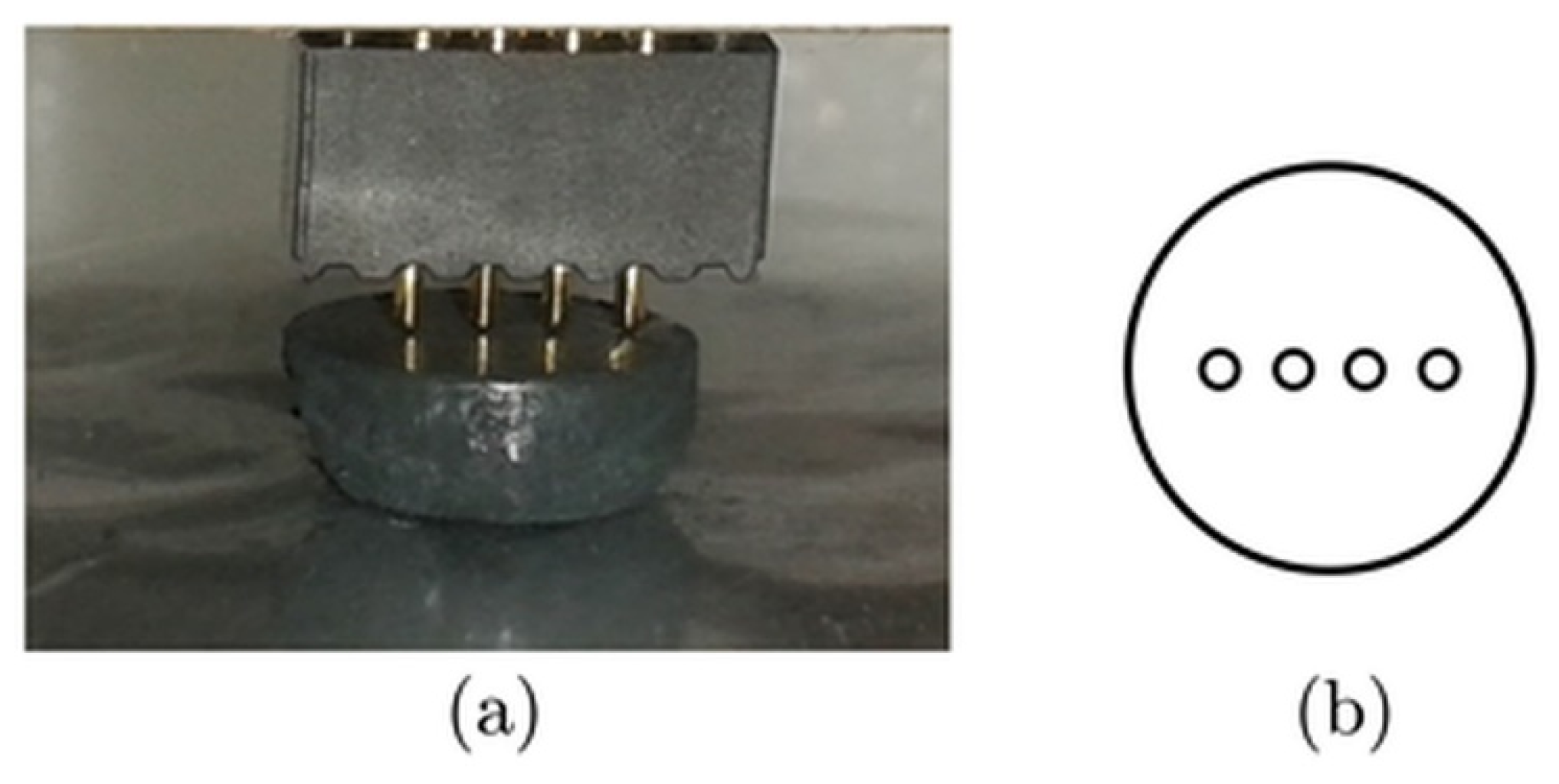
2. Materials and Methods
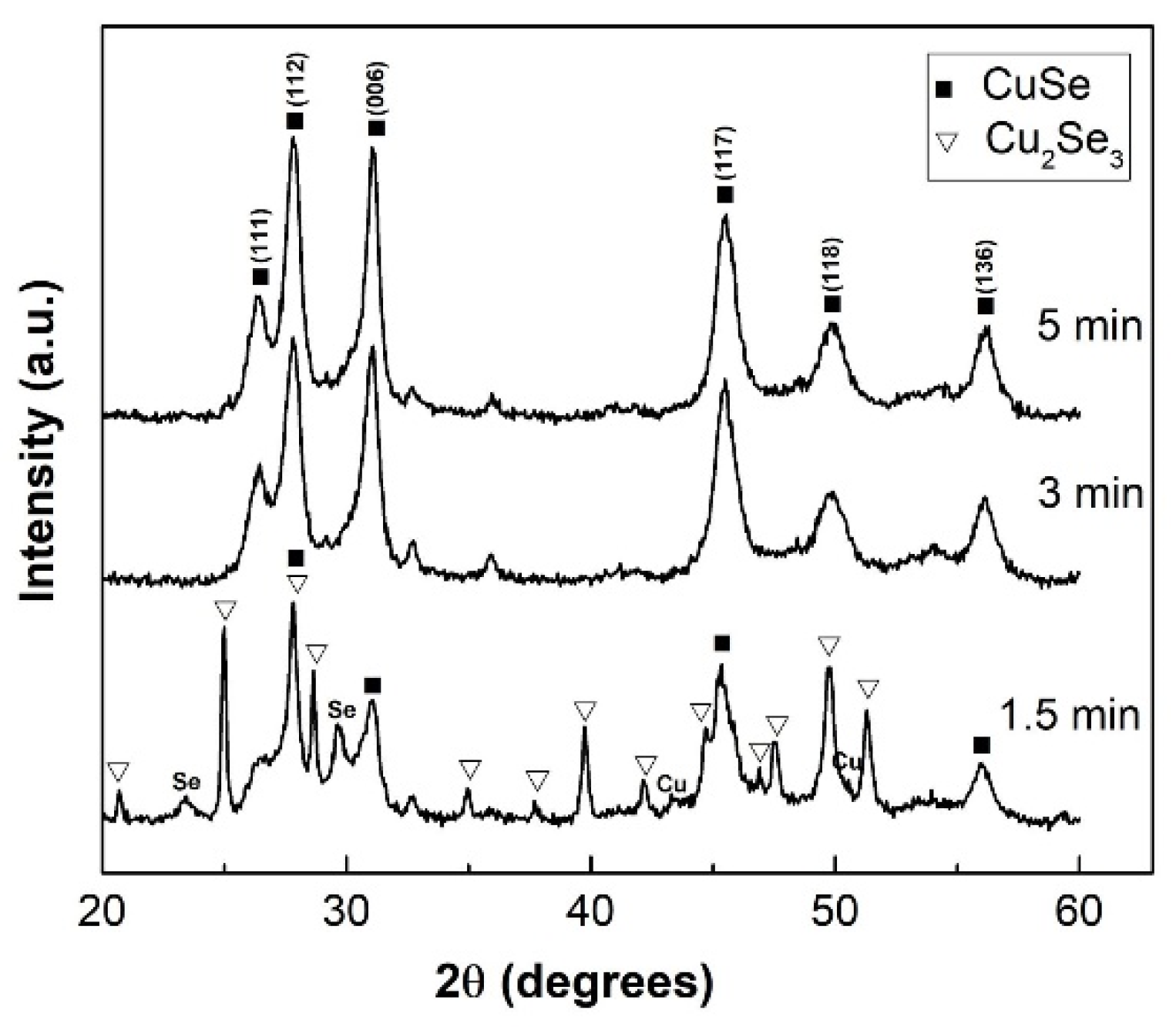
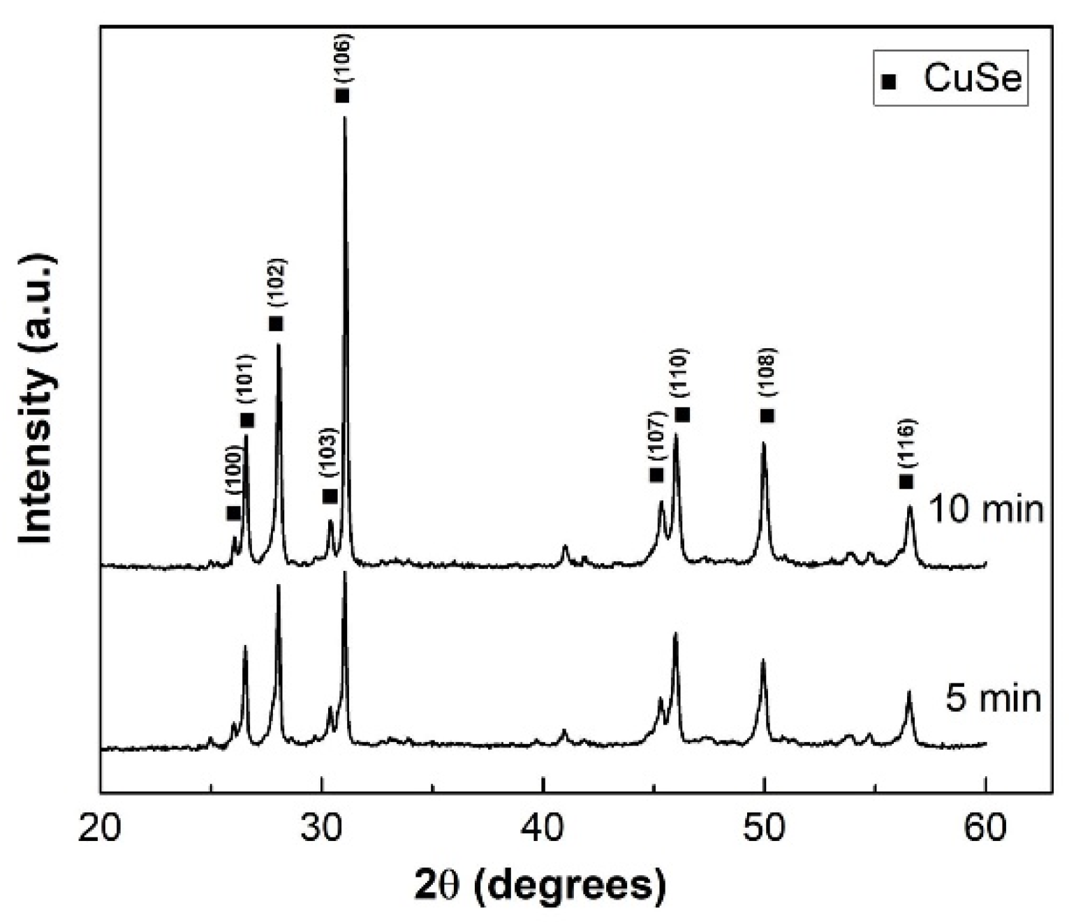
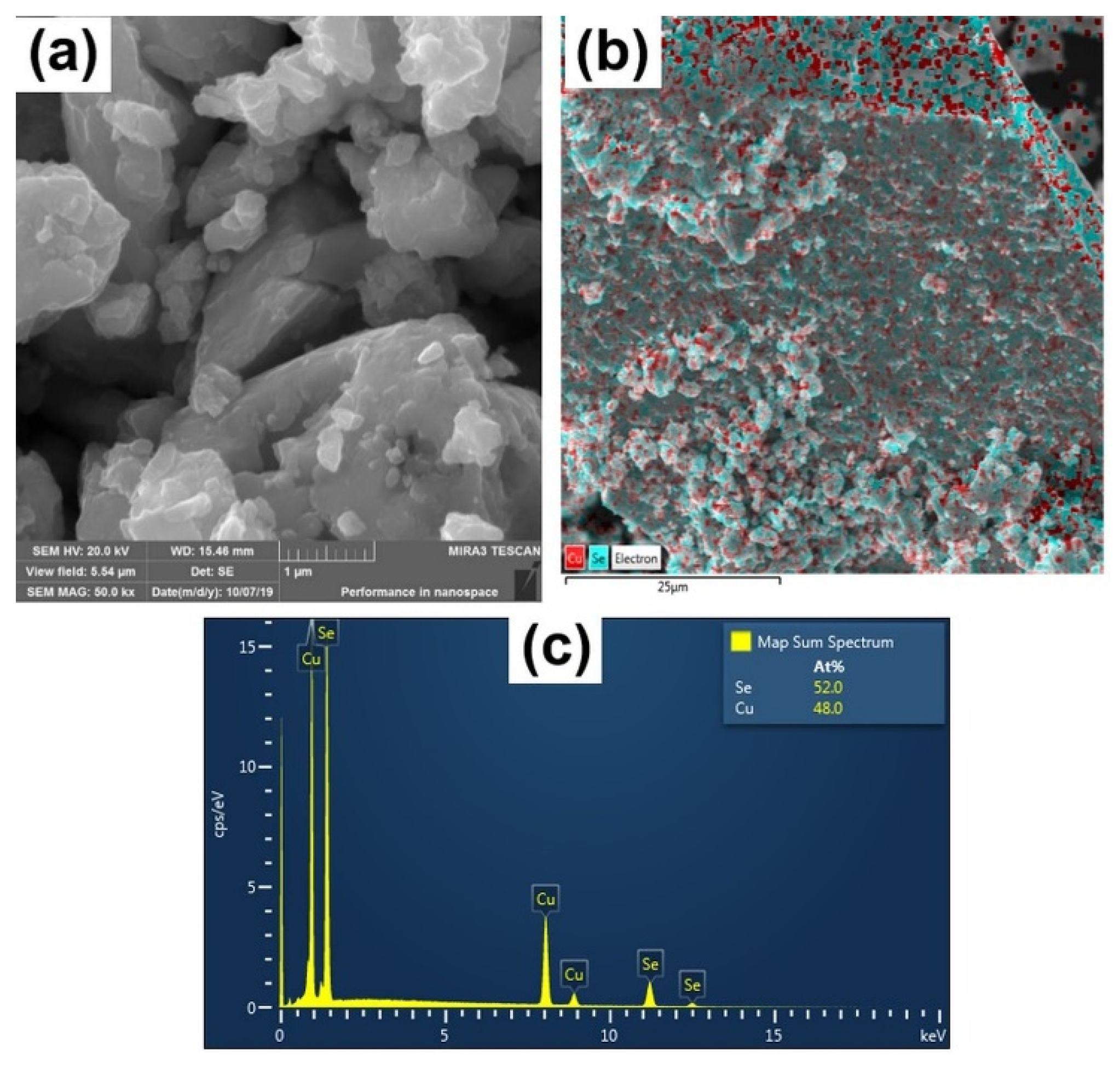
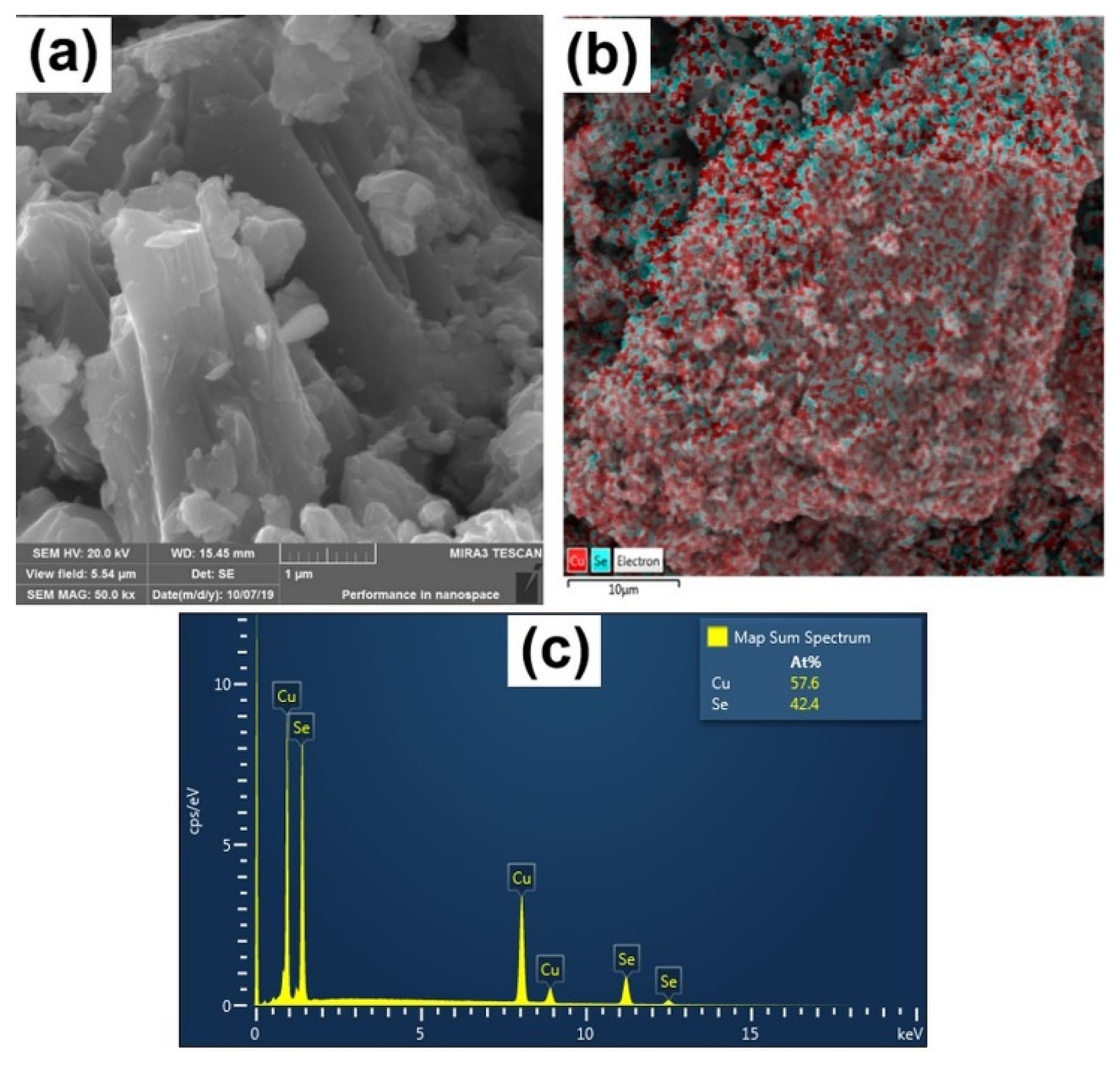
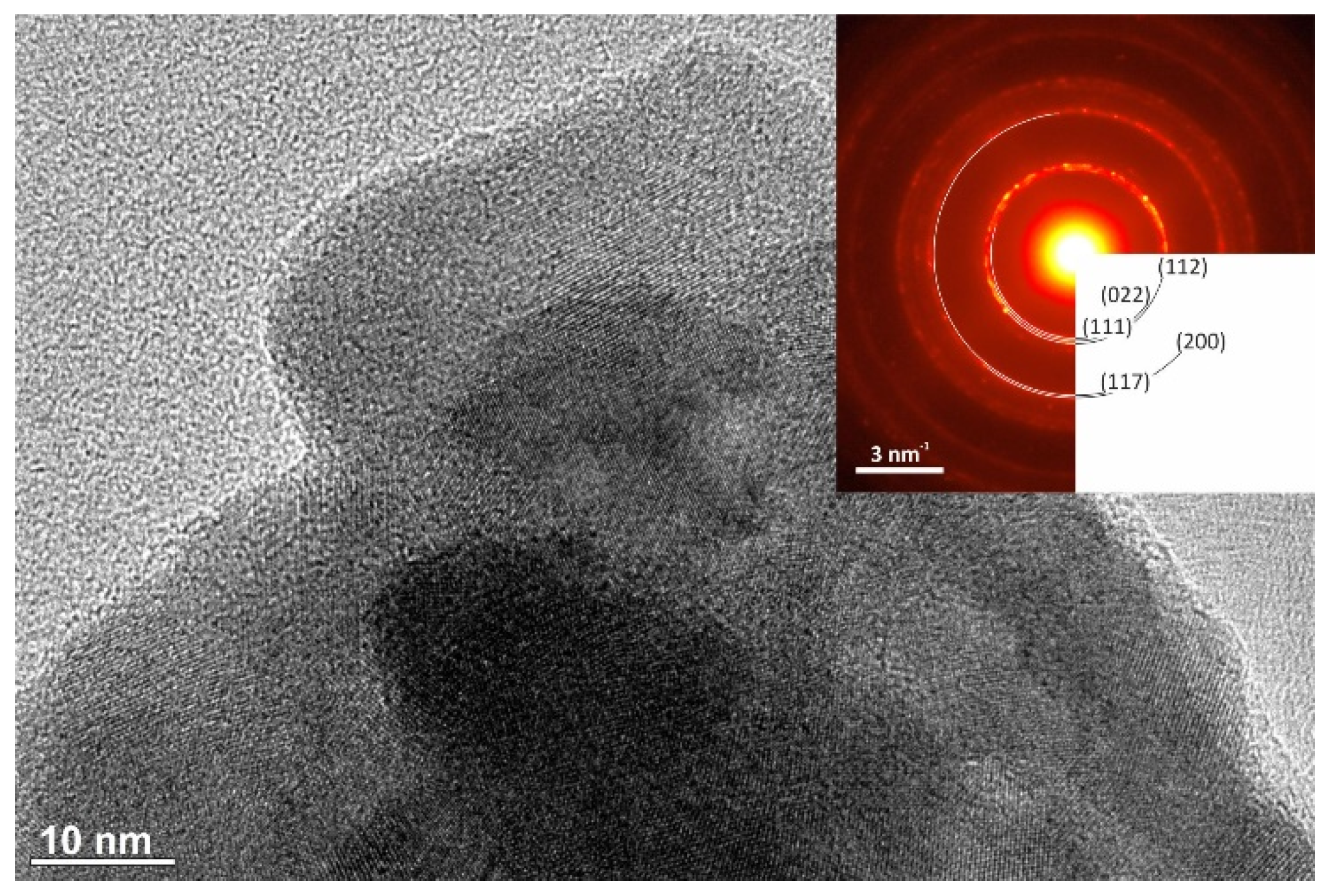
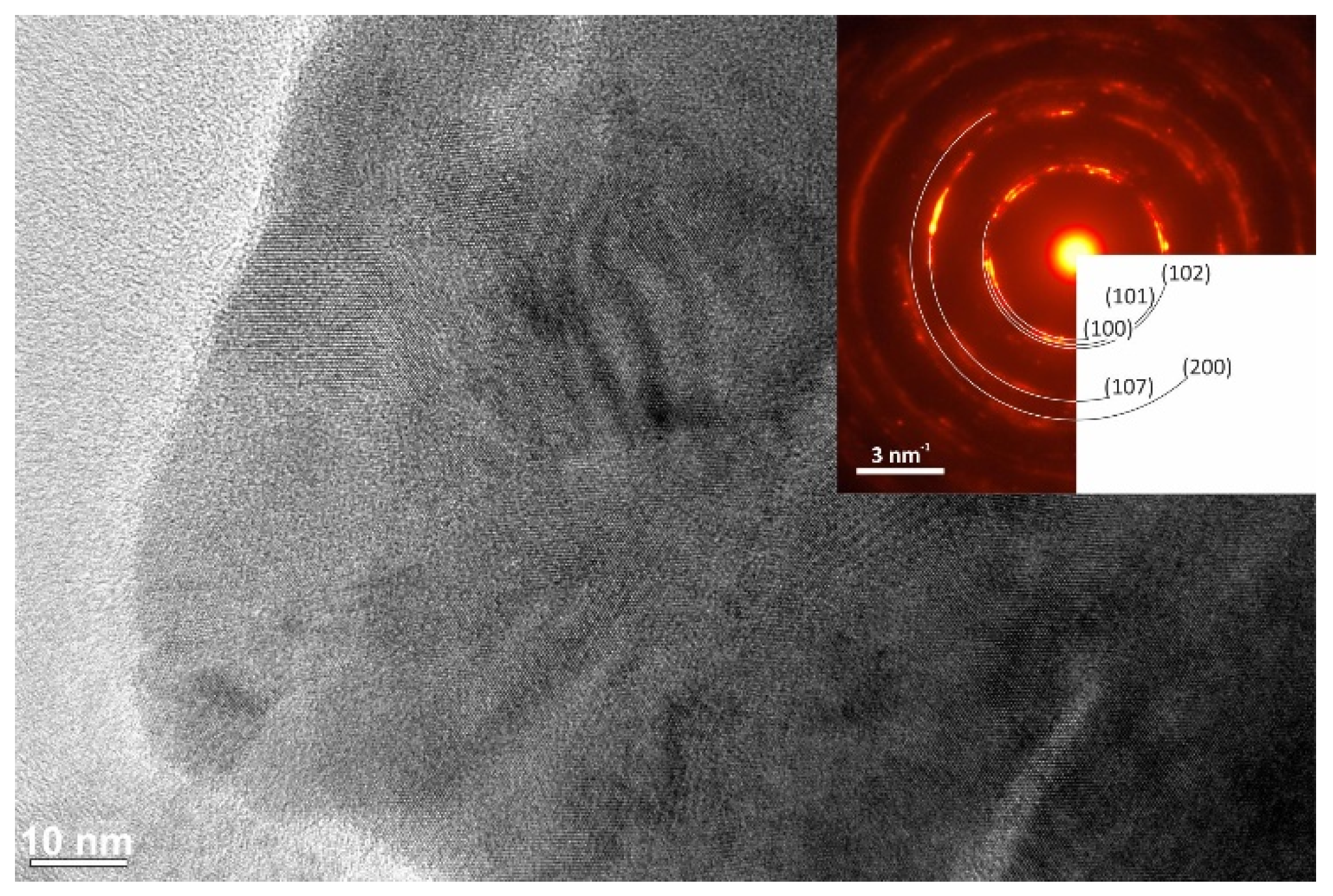
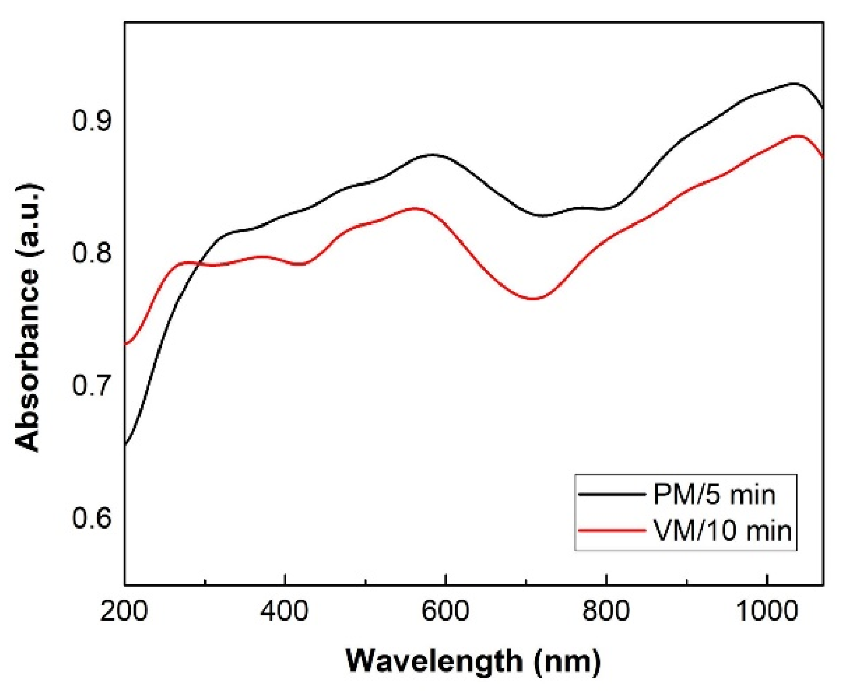
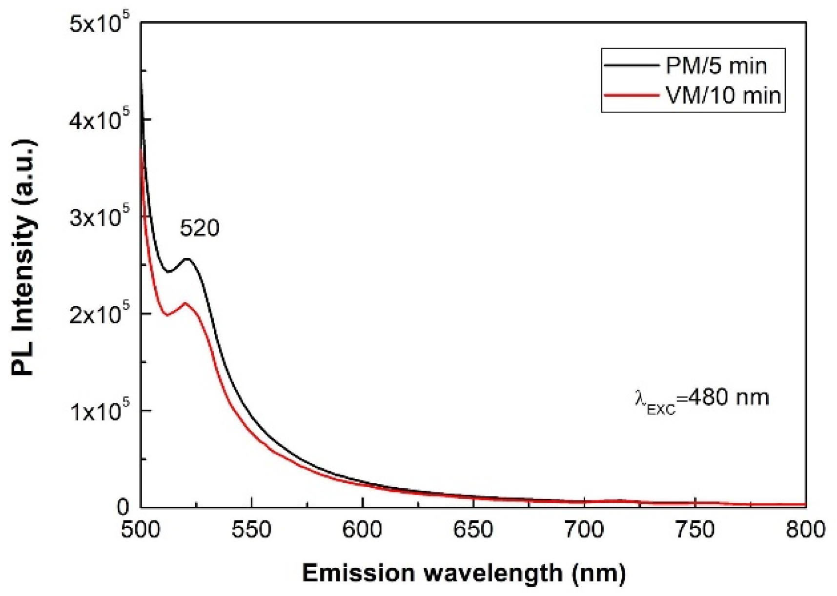
3. Results and Discussion
4. Conclusions
Author Contributions
Funding
Acknowledgments
Conflicts of Interest
References
- Gosavi, S.; Deshpande, N.; Gudage, Y.; Sharma, R. Physical, optical and electrical properties of copper selenide (CuSe) thin films deposited by solution growth technique at room temperature. J. Alloys Compd. 2008, 448, 344–348. [Google Scholar] [CrossRef]
- Hamilton, C.; Flood, D.; Barron, A. Thin film CdSe/CuSe photovoltaic on a flexible single walled carbon nanotube substrate. Phys. Chem. Chem. Phys. 2013, 15, 3930–3938. [Google Scholar] [CrossRef] [PubMed]
- Moloto, N.; Puggens, H.; Govindraju, S.; Rakgalakane, B.; Kalenga, M. Schottky solar cells: Anisotropic versus isotropic CuSe nanocrystals. Thin Solid Films 2013, 531, 446–450. [Google Scholar] [CrossRef]
- Gurin, V.; Prakapenka, V.; Kovalenko, D.; Alexeenko, A. Sol-gel derived silica films with ultrafine copper, copper sulfide and copper selenide particles. J. Sol Gel Sci. Technol. 2003, 26, 961–966. [Google Scholar] [CrossRef]
- Zyoud, A.; Murtada, K.; Kwon, H.; Choi, H.; Kim, T.; Helal, M.; Faroun, M.; Bsharat, H.; Park, D.; Hilal, H. Copper selenide film electrodes prepared by combined electrochemical/chemical bath depositions with high photo-electrochemical conversion efficiency and stability. Solid State Sci. 2018, 75, 53–62. [Google Scholar] [CrossRef]
- Korzhuev, M. Dufour effect in superionic copper selenide. Phys. Solid State 1998, 40, 217–219. [Google Scholar] [CrossRef]
- Xue, M.; Zhou, Y.; Zhang, B.; Yu, L.; Zhang, H.; Fu, Z. Fabrication and electrochemical characterization of copper selenide thin films by pulsed laser deposition. J. Electrochem. Soc. 2006, 153, A2262–A2268. [Google Scholar] [CrossRef]
- Su, H.; Xie, Y.; Li, B.; Qian, Y. A simple, convenient, mild hydrothermal route to nanocrystalline CuSe and Ag2Se. Mater. Res. Bull. 2000, 35, 465–469. [Google Scholar] [CrossRef]
- Li, H.; Zhu, Y.; Avivi, S.; Palchik, O.; Xiong, J.; Koltypin, Y.; Palchik, V.; Gedanken, A. Sonochemical process for the preparation of alpha-CuSe nanocrystals and flakes. J. Mater. Chem. 2002, 12, 3723–3727. [Google Scholar] [CrossRef]
- Vinod, T.; Jin, X.; Kim, J. Hexagonal nanoplatelets of CuSe synthesized through facile solution phase reaction. Mater. Res. Bull. 2011, 46, 340–344. [Google Scholar] [CrossRef]
- Liu, Y.; Wang, F.; Xiao, Y.; Peng, H.; Zhong, H.; Liu, Z.; Pan, G. Facile microwave-assisted synthesis of klockmannite CuSe nanosheets and their exceptional electrical properties. Sci. Rep. 2014, 4, 5998. [Google Scholar] [CrossRef] [PubMed]
- Bhuse, V.; Hankare, P.; Garadkar, K.; Khomane, A. A simple, convenient, low temperature route to grow polycrystalline copper selenide thin films. Mater. Chem. Phys. 2003, 80, 82–88. [Google Scholar] [CrossRef]
- Yakuphanoglu, F.; Viswanathan, C. Electrical conductivity and single oscillator model properties of amorphous CuSe semiconductor thin film. J. Non Cryst. Solids 2007, 353, 2934–2937. [Google Scholar] [CrossRef]
- Nelson, P.; Arthi, R.; Kaman, R.; Selyan, T.; Ajitha, E.; Ashina, A.; Vidhya, B. Influence of heat treatment on the properties of thermally evaporated copper selenide thin films. Mater. Lett. 2018, 223, 14–16. [Google Scholar] [CrossRef]
- Ezenwa, I.A.; Okereke, N.A.; Okoli, L.N. Electrical properties of copper selenide thin film. IPASJ Int. J. Electr. Eng. 2013, 1, 4. [Google Scholar]
- Thirumavalavan, S.; Mani, K.; Sagadevan, S. Investigation of the structural, optical and electrical properties of copper selenide thin films. Mater. Res. Ibero Am. J. Mater. 2015, 18, 1000–1007. [Google Scholar] [CrossRef]
- Sandoval-Paz, M.; Rodriguez, C.; Porcile-Saavedra, P.; Trejo-Cruz, C. Study of the crystallographic phase change on copper (I) selenide thin films prepared through chemical bath deposition by varying the pH of the solution. J. Solid State Chem. 2016, 239, 106–112. [Google Scholar] [CrossRef]
- Ramesh, K.; Thanikaikarasan, S.; Bharathi, B. Structural, morphological and optical properties of copper selenide thin films. Int. J. ChemTech Res. 2014, 6, 5408–5411. [Google Scholar]
- Petrovic, M.; Gilic, M.; Cirkovic, J.; Romčevic, M.; Romčevic, N.; Trajic, J.; Yahia, I. Optical properties of CuSe thin films—Band gap determination. Sci. Sinter. 2017, 49, 167–174. [Google Scholar] [CrossRef]
- Friscic, T.; Mottillo, C.; Titi, H.M. Mechanochemistry for Synthesis. Angew. Chem. Int. Ed. 2020, 59, 1018–1029. [Google Scholar] [CrossRef]
- James, S.L.; Adams, C.J.; Bolm, C.; Braga, D.; Collier, P.; Friščić, T.; Grepioni, F.; Harris, K.D.M.; Hyett, G.; Jones, W.; et al. Mechanochemistry: Opportunities for new and cleaner synthesis. Chem. Soc. Rev. 2012, 41, 413–447. [Google Scholar] [CrossRef] [PubMed]
- Baláž, P.; Achimovičová, M.; Baláž, M.; Billik, P.; Cherkezova-Zheleva, Z.; Criado, J.M.; Delogu, F.; Dutková, E.; Gaffet, E.; Gotor, F.J.; et al. Hallmarks of mechanochemistry: From nanoparticles to technology. Chem. Soc. Rev. 2013, 42, 7571–7637. [Google Scholar] [CrossRef]
- Ohtani, T.; Motoki, M.; Koh, K.; Ohshima, K. Synthesis of binary copper chalcogenides by mechanical alloying. Mater. Res. Bull. 1995, 30, 1495–1504. [Google Scholar] [CrossRef]
- Milman, V. Klockmannite, CuSe: Structure, properties and phase stability from ab initio modeling. Acta Crystallogr. B 2002, 58, 437–447. [Google Scholar] [CrossRef]
- Stolen, S.; Fjellvag, H.; Gronvold, F.; Sipowska, J.; Westrum, E. Heat capacity, structural and thermodynamic properties of synthetic klockmannite CuSe at temperatures from 5 K to 652.7 K. Enthalpy of decomposition. J. Chem. Thermodyn. 1996, 28, 753–766. [Google Scholar] [CrossRef]
- Baláž, P.; Baláž, M.; Achimovičová, M.; Bujňáková, Z.; Dutková, E. Chalcogenide mechanochemistry in materials science: Insight into synthesis and applications (a review). J. Mater. Sci. 2017, 52, 11851–11890. [Google Scholar] [CrossRef]
- Baláž, P.; Hegedus, M.; Baláž, M.; Daneu, N.; Siffalovic, P.; Bujňáková, Z.; Tóthová, E.; Tešinský, M.; Achimovičová, M.; Briančin, J.; et al. Photovoltaic materials: Cu2ZnSnS4 (CZTS) nanocrystals synthesized via industrially scalable, green, one-step mechanochemical process. Prog. Photovolt. Res. Appl. 2019, 27, 798–811. [Google Scholar] [CrossRef]
- Baláž, P.; Guilmeau, E.; Daneu, N.; Dobrozhan, O.; Baláž, M.; Hegedus, M.; Barbier, T.; Achimovičová, M.; Kaňuchová, M.; Briančin, J. Tetrahedrites synthesized via scalable mechanochemical process and spark plasma sintering. J. Eur. Ceram. Soc. 2020, 40, 1922–1930. [Google Scholar] [CrossRef]
- Achimovičová, M.; Dutková, E.; Tóthová, E.; Bujňáková, Z.; Briančin, J.; Kitazono, S. Structural and optical properties of nanostructured copper sulfide semiconductor synthesized in an industrial mill. Front. Chem. Sci. Eng. 2019, 13, 164–170. [Google Scholar] [CrossRef]
- Hegedüs, M.; Baláž, M.; Tešinský, M.; Sayagués, M.J.; Šiffalovič, P.; Kruľáková, M.; Briančin, J.; Fabián, M. Scalable synthesis of potential solar cell absorber Cu2SnS3 (CTS) from nanoprecursors. J. Alloys Compd. 2018, 768, 1006–10015. [Google Scholar] [CrossRef]
- Baláž, P.; Hegedüs, M.; Achimovičová, M.; Baláž, M.; Tešinský, M.; Dutková, E.; Kaňuchová, M.; Briančin, J. Semi-industrial green mechanochemical syntheses of solar cell absorbers based on quaternary sulfides. ACS Sust. Chem. Eng. 2018, 6, 2132–2141. [Google Scholar] [CrossRef]
- Baláž, P.; Hegedüs, M.; Reece, M.; Zhang, R.; Su, T.; Škorvánek, I.; Briančin, J.; Baláž, M.; Mihálik, M.; Tešinský, M.; et al. Mechanochemistry for thermoelectrics: Nanobulk Cu6Fe2SnS8/Cu2FeSnS4 composite synthesized in an industrial mill. J. Electron. Mater. 2019, 48, 1846–1856. [Google Scholar]
- Baláž, P. Mechanochemistry in Nanoscience and Minerals Engineering; Springer: Berlin/Heidelberg, Germany, 2008. [Google Scholar]
- Baláž, M.; Bujňáková, Z.; Achimovičová, M.; Tešinský, M.; Baláž, P. Simultaneous valorization of polyvinyl chloride and eggshell wastes by a semi-industrial mechanochemical approach. Environ. Res. 2019, 170, 332–336. [Google Scholar] [CrossRef]
- Heegn, H.P. Mühlen als Mechanoreaktoren. Chem. Ing. Tech. 2001, 73, 1529–1539. [Google Scholar] [CrossRef]
- Pietsch, H.E.E. (Ed.) Gmelin’s Handbook of Inorganic Chemistry, 8th ed.; Springer: Berlin/Heidelberg, Germany, 1955; p. 710. [Google Scholar]
- Coelho, A.A. TOPAS and TOPAS-Academic: An optimization program integrating computer algebra and crystallographic objects written in C plus. J. Appl. Crystallogr. 2018, 51, 210–218. [Google Scholar] [CrossRef]
- Evans, J.S.O. Advanced Input Files & Parametric Quantitative Analysis Using Topas. Mater. Sci. Forum 2010, 651, 1–9. [Google Scholar] [CrossRef]
- Topsoe, H. Geometric correction factors in four point resistivity measurement. Semicond Div. 1968, 472-13, 63. [Google Scholar]
- Kumar, V.; Kelekanjeri, G.; Gerhardt, R. A closed-form solution for the computation of geometric correction factors for four-point resistivity measurements on cylindrical specimens. Meas. Sci. Technol. 2008, 19, 025701. [Google Scholar] [CrossRef]
- Tauc, J.; Grigorovici, R.; Vancu, A. Optical properties and electronic structure of amorphous germanium. Phys. Status Solidi 1966, 15, 627. [Google Scholar] [CrossRef]
- Pankove, J.I. Optical Processes in Semiconductors; Prentice-Hall: Englewood Cliffs, NJ, USA, 1971; p. 422. [Google Scholar]
- Malik, M.; O’Brien, P.; Revaprasadu, N. A novel route for the preparation of CuSe and CuInSe2 nanoparticles. Adv. Mater. 1999, 11, 1441–1444. [Google Scholar] [CrossRef]
- Arellano-Tanori, O.; Acosta-Enriquez, M.; Ochoa-Landin, R.; Iniguez-Palomares, R.; Mendivil-Reynoso, T.; Flores-Acosta, M.; Castillo, S. Copper-selenide and copper-telluride composites powders synthesized by ionic exchange. Chalcogenide Lett. 2014, 11, 13–19. [Google Scholar]
- Jing, L.; Qu, Y.; Wang, B.; Li, S.; Jiang, B.; Yang, L.; Fu, W.; Fu, H.; Sun, J. Review of photoluminescence performance of nano-sized semiconductor materials and its relationships with photocatalytic activity. Sol. Energ. Mater. Sol. C 2006, 90, 1773–1787. [Google Scholar] [CrossRef]
- Kaviyarasu, K.; Ayeshamariam, A.; Manikandan, E.; Kennedy, J.; Ladchumananandasivam, R.; Gomes, U.; Jayachandran, M.; Maaza, M. Solution processing of CuSe quantum dots: Photocatalytic activity under RhB for UV and visible-light solar irradiation. Mater. Sci. Eng. B 2016, 210, 1–9. [Google Scholar] [CrossRef]
- Hou, X.; Xie, P.; Xue, S.; Feng, H.; Li, L.; Liu, Z.; Zou, R. The study of morphology-controlled synthesis and the optical properties of CuSe nanoplates based on the hydrothermal method. Mater. Sci. Semicond. Process. 2018, 79, 92–98. [Google Scholar] [CrossRef]
- Xue, L.; Zhang, Z.; Shen, W.; Ma, H.; Zhang, Y.; Fang, C.; Jia, X. Thermoelectric performance of Cu2Se bulk materials by high-temperature and high-pressure synthesis. J. Mater. 2019, 5, 103–110. [Google Scholar] [CrossRef]
- Bakonyi, I.; Isnaini, V.; Kolonits, T.; Czigany, Z.; Gubicza, J.; Varga, L.; Toth-Kadar, E.; Pogany, L.; Peter, L.; Ebert, H. The specific grain-boundary electrical resistivity of Ni. Phil. Mag. 2019, 99, 1139–1162. [Google Scholar] [CrossRef]


| CuSe-PM | CuSe-VM | |
|---|---|---|
| Amount of hexagonal CuSe (Pmmc/63) (%) | 78.2 ± 0.8 | 98.4 ± 0.7 |
| Crystallite size (nm) | 24 ± 2 | 64 ± 2 |
| Strain (%) | 1.45 ± 0.07 | not contributing |
| Unit cell parameter a (nm) | 0.3972 ± 0.0017 | 0.3941 ± 0.0003 |
| Unit cell parameter c (nm) | 1.7215 ± 0.0074 | 1.7232 ± 0.0017 |
| CuSe Product/Milling Time | SA (m2 × g−1) | x50 (μm) |
|---|---|---|
| PM/5 min | 1.60 | 9.29 |
| VM/10 min | 1.02 | 44.78 |
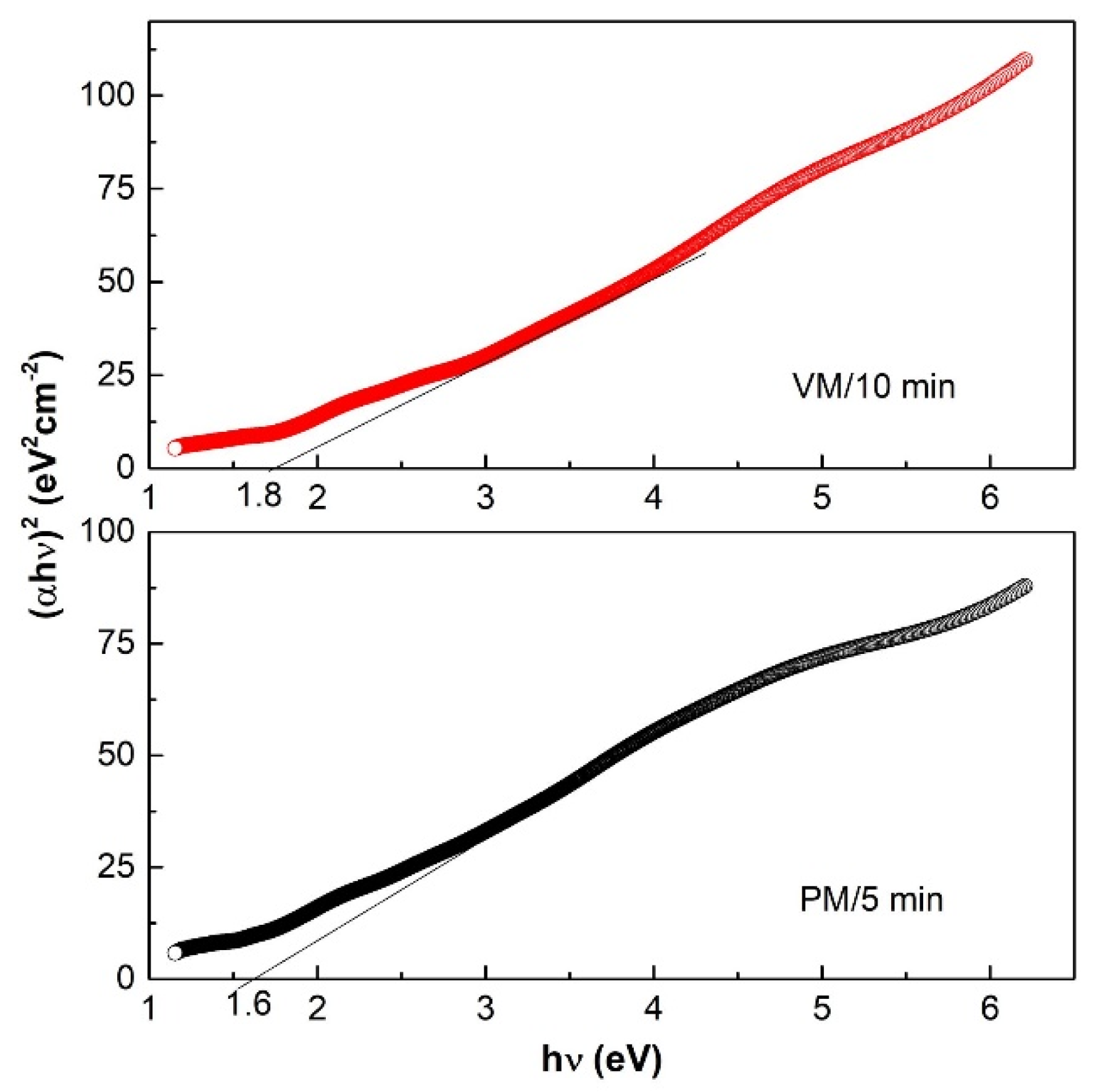
| Method of Preparation | Direct Band Gap (eV) | Reference |
|---|---|---|
| Microwave-assisted synthesis | 1.36 | [11] |
| Thermal evaporation | 1.54–2.54 | [14] |
| Single source-route | 1.63–1.77 | [43] |
| Solution growth technique | 2.03 | [1] |
| Electrodeposition | 2.10 | [18] |
| Electrodeposition/chemical bad deposition | 2.20 | [5] |
| Chemical bad deposition | 2.40 | [16] |
| Vacuum evaporation method | ~2.70 | [19] |
| Ionic exchange chemical reaction | 2.79 | [44] |
| Thermal evaporation technique | 3.55 | [13] |
| Mechanochemical synthesis-PM | 1.6 | [This work] |
| Mechanochemical synthesis-VM | 1.8 | [This work] |
| CuSe Product | Mean | StandardDev | Median | |
|---|---|---|---|---|
| Sheet resistance (Ω/square) | PM/5 min | 0.70 | 0.02 | 0.70 |
| VM/10 min | 0.46 | 0.02 | 0.46 | |
| Resistivity (mΩ m) | PM/5 min | 1.24 | 0.04 | 1.24 |
| VM/10 min | 1.20 | 0.05 | 1.20 | |
| Conductivity (S/m) | PM/5 min | 808.19 | 27.81 | 807.75 |
| VM/10 min | 831.80 | 32.71 | 831.94 |
Publisher’s Note: MDPI stays neutral with regard to jurisdictional claims in published maps and institutional affiliations. |
© 2020 by the authors. Licensee MDPI, Basel, Switzerland. This article is an open access article distributed under the terms and conditions of the Creative Commons Attribution (CC BY) license (http://creativecommons.org/licenses/by/4.0/).
Share and Cite
Achimovičová, M.; Baláž, M.; Girman, V.; Kurimský, J.; Briančin, J.; Dutková, E.; Gáborová, K. Comparative Study of Nanostructured CuSe Semiconductor Synthesized in a Planetary and Vibratory Mill. Nanomaterials 2020, 10, 2038. https://doi.org/10.3390/nano10102038
Achimovičová M, Baláž M, Girman V, Kurimský J, Briančin J, Dutková E, Gáborová K. Comparative Study of Nanostructured CuSe Semiconductor Synthesized in a Planetary and Vibratory Mill. Nanomaterials. 2020; 10(10):2038. https://doi.org/10.3390/nano10102038
Chicago/Turabian StyleAchimovičová, Marcela, Matej Baláž, Vladimír Girman, Juraj Kurimský, Jaroslav Briančin, Erika Dutková, and Katarína Gáborová. 2020. "Comparative Study of Nanostructured CuSe Semiconductor Synthesized in a Planetary and Vibratory Mill" Nanomaterials 10, no. 10: 2038. https://doi.org/10.3390/nano10102038
APA StyleAchimovičová, M., Baláž, M., Girman, V., Kurimský, J., Briančin, J., Dutková, E., & Gáborová, K. (2020). Comparative Study of Nanostructured CuSe Semiconductor Synthesized in a Planetary and Vibratory Mill. Nanomaterials, 10(10), 2038. https://doi.org/10.3390/nano10102038