Influence of SERS Activity of SnSe2 Nanosheets Doped with Sulfur


Abstract
:1. Introduction
2. Experiment
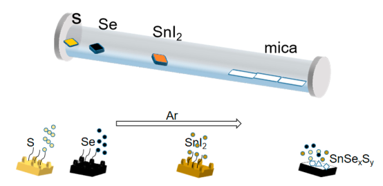
2.1. Synthesis of the SnSexSy Nanosheets
2.2. Characterization of SnSexSy Nanosheets
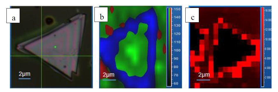
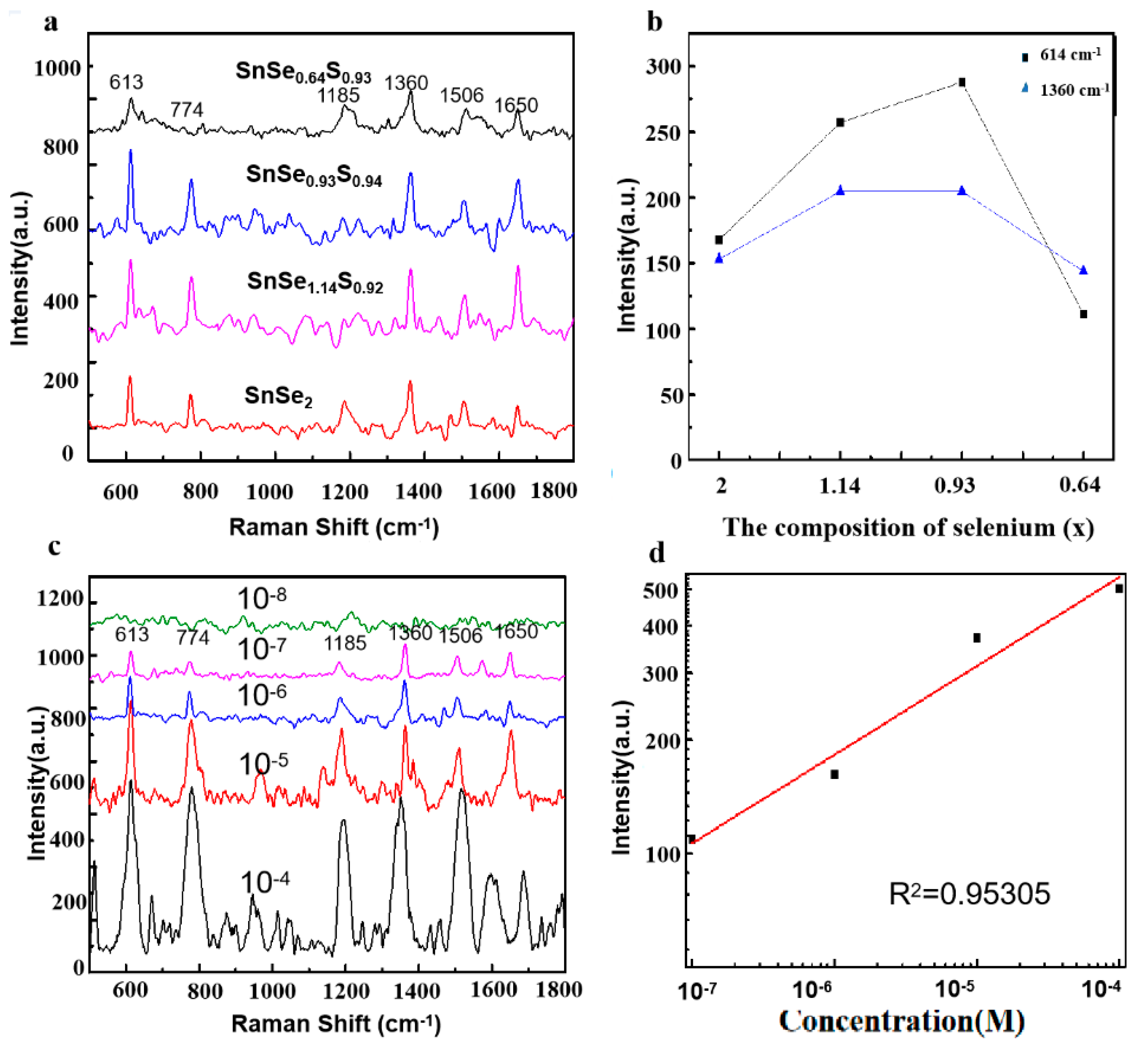
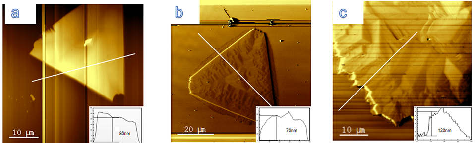
3. Result and Discussion
4. Conclusions
Supplementary Materials
Author Contributions
Funding
Conflicts of Interest
References
- Gambucci, M.; Cambiotti, E.; Sassi, P.; Latterini, L. Multilayer Gold-Silver Bimetallic Nanostructures to Enhance SERS Detection of Drugs. Molecules 2020, 25, 3405. [Google Scholar] [CrossRef]
- Barbillon, G. Latest Novelties on Plasmonic and Non-Plasmonic Nanomaterials for SERS Sensing. Nanomaterials 2020, 10, 1200. [Google Scholar] [CrossRef]
- Yang, Y.T.; Hsu, I.L.; Cheng, T.Y.; Wu, W.J.; Lee, C.W.; Li, T.J.; Cheung, C.I.; Chin, Y.C.; Chen, H.C.; Chiu, Y.C.; et al. Off-Resonance SERS Nanoprobe-Targeted Screen of Biomarkers for Antigens Recognition of Bladder Normal and Aggressive Cancer Cells. Anal. Chem. 2019, 91, 8213–8220. [Google Scholar] [CrossRef] [PubMed]
- Nowicka, A.B.; Czaplicka, M.; Kowalska, A.A.; Szymborski, T.; Kamińska, A. Flexible PET/ITO/Ag SERS Platform for Label-Free Detection of Pesticides. Biosensors 2019, 9, 111. [Google Scholar] [CrossRef] [PubMed] [Green Version]
- Lee, C.W.; Ko, H.; Chang, S.H.G.; Huang, C.C. Invisible-ink-assisted pattern and written surface-enhanced Raman scattering substrates for versatile chem/biosensing platforms. Green Chem. 2018, 20, 5318–5326. [Google Scholar] [CrossRef]
- Van Der Zande, A.M.; Huang, P.Y.; Chenet, D.A.; Berkelbach, T.C.; You, Y.; Lee, G.H.; Heinz, T.F.; Reichman, D.R.; Muller, D.A.; Hone, J.C. Grains and grain boundaries in highly crystalline monolayer molybdenum disulphide. Nat. Mater. 2013, 12, 554–561. [Google Scholar] [CrossRef] [Green Version]
- Choi, W.; Cho, M.Y.; Konar, A.; Lee, J.H.; Cha, G.B.; Hong, S.C.; Kim, S.; Kim, J.; Jena, D.; Joo, J.; et al. High-detectivity multilayer MoS2 phototransistors with spectral response from ultraviolet to infrared. Adv. Mater. 2012, 24, 5832–5836. [Google Scholar] [CrossRef]
- Tonndorf, P.; Schmidt, R.; Böttger, P.; Zhang, X.; Börner, J.; Liebig, A.; Albrecht, M.; Kloc, C.; Gordan, O.; Zahn, D.R.; et al. Photoluminescence emission and Raman response of monolayer MoS2, MoSe2, and WSe2. Opt. Express 2013, 21, 4908–4916. [Google Scholar] [CrossRef]
- Xia, J.; Huang, X.; Liu, L.Z.; Wang, M.; Wang, L.; Huang, B.; Zhu, D.D.; Li, J.J.; Gu, C.Z.; Meng, X.M. CVD synthesis of large-area, highly crystalline MoSe2 atomic layers on diverse substrates and application to photodetectors. Nanoscale 2014, 6, 8949–8955. [Google Scholar] [CrossRef] [Green Version]
- Baek, J.; Yin, D.; Liu, N.; Omkaram, I.; Jung, C.; Im, H.; Hong, S.; Kim, S.M.; Hong, Y.K.; Hur, J.; et al. A Highly sensitive chemical gas detecting transistor based on highly crystalline CVD-grown MoSe2 fifilms. Nano Res. 2016, 10, 1861–1871. [Google Scholar] [CrossRef]
- Gao, Y.; Hong, Y.; Yin, L.; Wu, Z.; Yang, Z.; Chen, M.; Liu, Z.; Ma, T.; Sun, D.; Ni, Z.; et al. Ultrafast growth of high-quality monolayer WSe2 on Au. Adv. Mater. 2017, 29, 1700990. [Google Scholar] [CrossRef] [PubMed]
- Huang, J.; Pu, J.; Hsu, C.L.; Chiu, M.H.; Juang, Z.; Chang, Y.; Chang, W.; Iwasa, Y.; Takenobu, T.; Li, L. Large-area synthesis of highly crystalline WSe2 monolayers and device applications. ACS Nano 2013, 8, 923–930. [Google Scholar] [CrossRef] [PubMed] [Green Version]
- Late, D.J.; Liu, B.; Luo, J.; Yan, A.; Matte, H.R.; Grayson, M.; Rao, C.N.R.; Dravid, V.P. GaS and GaSe ultrathin layer transistors. Adv. Mater. 2012, 24, 3549–3554. [Google Scholar] [CrossRef] [PubMed]
- Hu, P.; Wang, L.; Yoon, M.; Zhang, J.; Feng, W.; Wang, X.; Wen, Z.; Idrobo, J.C.; Miyamoto, Y.; Geohegan, D.B.; et al. Highly responsive ultrathin GaS nanosheet photodetectors on rigid and flflexible substrates. Nano Lett. 2013, 13, 1649–1654. [Google Scholar] [CrossRef]
- Feng, W.; Zheng, W.; Cao, W.; Hu, P. Back gated multilayer InSe transistors with enhanced carrier mobilities via the suppression of carrier scattering from a dielectric interface. Adv. Mater. 2014, 26, 6587–6593. [Google Scholar] [CrossRef]
- Feng, W.; Wu, J.; Li, X.; Zheng, W.; Zhou, X.; Xiao, K.; Cao, W.; Yang, B.; Idrobo, J.C.; Basile, L.; et al. Ultrahigh photo-responsivity and detectivity in multilayer InSe nanosheets phototransistors with broadband response. J. Mater. Chem. C 2015, 3, 7022–7028. [Google Scholar] [CrossRef]
- Su, G.; Hadjiev, V.G.; Loya, P.E.; Zhang, J.; Lei, S.; Maharjan, S.; Dong, P.; Ajayan, P.M.; Lou, J.; Peng, H. Chemical vapor deposition of thin crystals of layered semiconductor SnS2 for fast photodetection application. Nano Lett. 2015, 15, 506–513. [Google Scholar] [CrossRef]
- Gonzalez, J.M.; Oleynik, I. Layer-dependent properties of SnS2 and SnSe2 two-dimensional materials. Phys. Rev. B 2016, 94, 125443. [Google Scholar] [CrossRef] [Green Version]
- Yu, P.; Yu, X.; Lu, W.; Lin, H.; Sun, L.; Du, K.; Liu, F.; Fu, W.; Zeng, Q.; Shen, Z.; et al. Fast photoresponse from 1T tin diselenide atomic layers. Adv. Funct. Mater. 2016, 26, 137–145. [Google Scholar] [CrossRef]
- Yu, P.; Yu, X.; Lu, W.; Lin, H.; Sun, L.; Du, K.; Liu, F.; Fu, W.; Zeng, Q.; Shen, Z.; et al. SnSe2 quantum dotsensitized solar cells prepared employing molecular metal chalcogenide as precursors. Adv. Funct. Mater. 2012, 48, 3324–3326. [Google Scholar]
- Huang, Y.; Chen, X.; Zhou, D.; Liu, H.; Wang, C.; Du, J.; Ning, L.; Wang, S. Stabilities, Electronic and Optical Properties of SnSe2(1−x)S2x Alloys: A First Principles Study. J. Phys. Chem. C 2016, 120, 5839–5847. [Google Scholar] [CrossRef]
- Zhang, Y.; Shi, Y.; Wu, M.; Zhang, K.; Man, B.; Liu, M. Synthesis and Surface-Enhanced Raman Scattering of Ultrathin SnSe2 Nanoflflakes by Chemical Vapor Deposition. Nanomaterials 2018, 8, 515. [Google Scholar] [CrossRef] [Green Version]
- Joseph, A.; Anjitha, C.R.; Aravind, A.; Aneesh, P.M. Structural, optical and magnetic properties of SnS2 nanoparticles and photo response characteristics of p-Si/n-SnS2 heterojunction diode. Appl. Surf. Sci. 2020, 528, 146977. [Google Scholar] [CrossRef]
- Güneri, E.; Göde, F.; Boyarbay, B.; Gümüş, C. Structural and optical studies of chemically deposited Sn2S3 thin films. Mater. Res. Bull. 2012, 47, 3738–3742. [Google Scholar] [CrossRef]
- Fernandes, P.A.; Sousa, M.G.; Salomé, P.M.P.; Leitão, J.P.; da Cunha, A.F. Thermodynamic pathway for the formation of SnSe and SnSe2 polycrystalline thin films by selenization of metal precursors. Cryst. Eng. Commun. 2013, 15, 10278–10286. [Google Scholar] [CrossRef] [Green Version]
- Shan, Y.; Zheng, Z.; Liu, J.; Yang, Y.; Li, Z.; Huang, Z.; Jiang, D. Niobium pentoxide: A promising surface-enhanced Raman scattering active semiconductor substrate. npj Comput. Mater. 2017, 3, 11. [Google Scholar] [CrossRef]
- Burton, L.A.; Whittles, T.J.; Hesp, D.; Linhart, W.M.; Skelton, J.M.; Hou, B.; Webster, R.F.; Odowd, G.; Reece, C.; Cherns, D.; et al. Electronic and optical properties of single crystal SnS2: An earth-abundant disulfide photocatalyst. J. Mater. Chem. A 2016, 4, 1312–1318. [Google Scholar] [CrossRef] [Green Version]


| No. | Ratio of S:Se in Source | Stoichiometry of Sample (%) | x | y | x + y | ||
|---|---|---|---|---|---|---|---|
| Sn | Se | S | |||||
| 0 | — | 33 | 67 | — | 2 | — | 2 |
| 1 | 1:20 | 32.78 | 37.27 | 29.95 | 1.14 | 0.92 | 2.06 |
| 2 | 1:10 | 34.80 | 32.24 | 32.95 | 0.93 | 0.94 | 1.87 |
| 3 | 7:10 | 38.91 | 25.07 | 36.02 | 0.64 | 0.93 | 1.57 |
© 2020 by the authors. Licensee MDPI, Basel, Switzerland. This article is an open access article distributed under the terms and conditions of the Creative Commons Attribution (CC BY) license (http://creativecommons.org/licenses/by/4.0/).
Share and Cite
Tian, Y.; Wei, H.; Xu, Y.; Sun, Q.; Man, B.; Liu, M. Influence of SERS Activity of SnSe2 Nanosheets Doped with Sulfur. Nanomaterials 2020, 10, 1910. https://doi.org/10.3390/nano10101910
Tian Y, Wei H, Xu Y, Sun Q, Man B, Liu M. Influence of SERS Activity of SnSe2 Nanosheets Doped with Sulfur. Nanomaterials. 2020; 10(10):1910. https://doi.org/10.3390/nano10101910
Chicago/Turabian StyleTian, Yuan, Haonan Wei, Yujie Xu, Qianqian Sun, Baoyuan Man, and Mei Liu. 2020. "Influence of SERS Activity of SnSe2 Nanosheets Doped with Sulfur" Nanomaterials 10, no. 10: 1910. https://doi.org/10.3390/nano10101910
APA StyleTian, Y., Wei, H., Xu, Y., Sun, Q., Man, B., & Liu, M. (2020). Influence of SERS Activity of SnSe2 Nanosheets Doped with Sulfur. Nanomaterials, 10(10), 1910. https://doi.org/10.3390/nano10101910