Article

Optimal Energy Management Scheme of Battery Supercapacitor-Based Bidirectional Converter for DC Microgrid Applications

by
Srinivas Punna
1,
Sujatha Banka
1 and
Surender Reddy Salkuti
2,*
1
Department of Electrical and Electronics Engineering, BVRIT HYDERABAD College of Engineering for Women, Hyderabad 500090, India
2
Department of Railroad and Electrical Engineering, Woosong University, Daejeon 34606, Korea
*
Author to whom correspondence should be addressed.
Information 2022, 13(7), 350; https://doi.org/10.3390/info13070350
Submission received: 16 May 2022 / Revised: 11 July 2022 / Accepted: 12 July 2022 / Published: 21 July 2022
(This article belongs to the Special Issue Intelligent Manufacturing and Informatization)

Abstract

:
Because of the splendid front of sustainable energy reassets in a DC Microgrid, it is profoundly willing to variances in energy age. A hybrid energy storage system (HESS) which includes a battery and a supercapacitor (SC) is used to decrease in-built fluctuations. The two different characteristics of the battery and supercapacitor make it a great match for HESS applications. The HESS is connected to the DC Microgrid through a bidirectional converter, which allows energy to be exchanged between the battery and supercapacitor. This paper discusses a converter presenting an approach for a double-input bidirectional converter. Related to this, a regulator was designed for use as a voltage regulation in a DC Microgrid. The designed controllers accelerated PV generation and load disturbance DC link voltage restoration, in addition to effective power balancing among the battery and the SC. The conventional PI, proposed PI, and predictive PI control techniques are effectively validated using MATLAB Simulink. Experimental findings with low power have been used to validate the operation of the predictive PI control technique. The DC grid voltage profile showed substantial improvement while using the predictive PI control in comparison with the proposed and conventional PI control techniques in terms of setting time and maximum peak overshoot.

1. Introduction

DC Microgrids are becoming very popular due to their reliability and ease of integration with renewable energy sources and the expansion of DC-compatible loads [1,2]. Because of the tremendous penetration of intermittent renewable strength reassets into a DC Microgrid, there is a power mismatch between the generation and load sides, causing DC bus voltage swings. To deal with this challenge, a variety of energy storage systems (ESS) of various sorts and qualities are used. The most popular ESS is the battery. In ESSs, batteries are prioritized for high energy density whereas supercapacitors are preferred for high power density [3,4]. Renewable energy sources require an ESS with a high energy density, but loads with a high-pulse requirement require an ESS with a high power density due to the nature of intermittent energy. As a result, to meet the aforementioned DC Microgrid requirements, a hybrid energy storage system (HESS) was developed by combining a battery with a supercapacitor [5,6,7,8,9,10,11,12]. A HESS also increases the steadiness of the power converter-based microgrid, which could in any other case be unstable [13] due to its low rotational inertia.
Various topologies of HESS are displayed to achieve the advantages of both a battery and a supercapacitor [14]. The most widely recognized HESS plan, which considers free control of both the battery and supercapacitor, is addressed in Figure 1a. It is feasible to trade energy between the part ESSs in the dynamic equal course of action of a HESS; for instance, the battery ESS can charge the supercapacitor ESS or the other way around. However, when energy is traded through a DC Microgrid, the lattice’s working requirements might be pushed past the ideal reach.
As displayed in Figure 1b, multiple-input bidirectional (MIBD) converters have more noteworthy energy trade execution between input sources contrasted with multiple single-input bidirectional DC (MSIBD) converters in dynamic equal mode. Subsequently, the previous is ideal for hybrid electric vehicles (HEVs) and DC Microgrids. The critical benefits of the MIBD converter over the MSIBD converter are (i) further developed energy trade between input sources, (ii) modular framework size, and (iii) lower converter cost [15].
A couple of input topologies had been proposed for interfacing more than one source with diverse characteristics. Numerous ESSs are associated with a three-winding high-frequency transformer, with each source associated through a full-bridge circuit [16]. In DC Microgrid applications, the number of switches required for a battery–supercapacitor HESS is eight, which may influence overall efficiency [17,18], described as an isolated multiport DC-DC converter that can handle power from numerous energy sources and provide it to a single load. The power transmission between the sources and the ESSs was not explored when the sources were replaced with ESSs. Isolated converters can handle a wide range of voltage levels and can ensure safety through isolation, but managing energy from many sources is more complicated than with non-isolated converters.
In the literature, there are multi-input non-isolated DC-DC bidirectional converters for connecting numerous sources [19,20,21,22,23,24,25,26,27,28,29,30,31,32], which provide substantially more flexibility in implementation and power regulation than isolated converters. The authors of [19] described and experimentally validated a process for constructing all possible double-input, single-output DC-DC converters for a system using the battery as one of the inputs. However, there was no consideration for bidirectional power flow between the two input ports, which is essential for the HESS in DC Microgrid applications. The authors of [20] presented a multi-input DC-DC converter with no power-sharing option between the input sources for several energy sources with varying characteristics. Benfei Wanga et al. [21] proposed a single inductor-based multi-port converter for a HESS. Since the Predictive control model is used in this paper, the computing and controller effort is significantly higher. Furthermore, the validity of the control approach requires SOC-based analysis.
Sivipriya et al. [22] proposed a rural electrification microgrid using PV and battery. Rasoul Faraji et al. [23] proposed a multiport hybrid energy system with PV and storage. If the battery is utilized alone, the stress on the battery will rise. Furthermore, the proposed converter is incompatible with SC applications. A multi-port converter for PV and batteries was also proposed by Yusuke Sato et al. [24]. The proposed circuit can integrate the battery with PV, but the battery would be under a lot of stress during various disturbances. Zhehan Yi et al. initiated a new control of an energy management system for a PV-Battery-based system for grid-connected and islanded operations [25]. In the proposed control strategy, the battery balances the power of the AC and DC Microgrid in all operational scenarios. In the proposed control strategy, the battery balances AC and DC Microgrid power at all times. Battery stress, system expense, and battery life cycle all rise as a result of this. The authors of [30] proposed a high-efficiency two-input interleaved converter for energy storage. The dual-input interleaved converter circuit, on the other hand, has a sophisticated control approach that requires eight switches. Multi-input converters for grid-tied and/or solar applications are mentioned in [31,32,33]. Multi-input systems, as seen in [34,35,36,37,38], are also used in HEV applications. All the preceding multiple-input converter topologies, however, find it hard to keep SoCSC within predefined limits, rendering SC protection difficult.
Due to the fact that there are numerous publications on multi-input bidirectional converters in the literature, their controller development methods have received little attention. A multi-input bidirectional DC-DC converter is used to connect the HESS to the DC Microgrid, as proposed in [39]. The converter in [39,40,41,42,43,44] has been normalized in operation to allow HESS operation in DC Microgrid applications. One striking characteristic of this converter is that it activates all of the switches that use zero voltage switching (ZVS), potentially increasing its efficiency. Apart from regulating HESS charging and discharging, the unified controller may also share current between the battery and supercapacitor, reducing current stress on the former and increasing its lifespan. The total HESS current is bifurcated (charging/discharging), with the power density element supercapacitor supplying the high-frequency component and the energy density unit battery supplying the average or low-frequency current. The architecture of two-input bidirectional converter configuration of HESS aided RES is illustrated in Figure 2. The following are the paper’s major contributions:
This research work proposes a DC Microgrid voltage stabilization based on multi-input converters.
A comprehensive controller is introduced for the design and analysis of a HESS-based multiple-input bidirectional converter. For a multi-input converter, the small-signal model-based-provided controller ensures stability in all working areas.
The execution of an energy management system for a multiple-input bi-directional converter with HESS is introduced for different PV and load conditions. The EMS can undoubtedly follow the SC SoC and empower various modes to guarantee safe activity.
The primary benefit of the planned double-input bidirectional converter is its energy trade mode, which permits charging the SC freely from the battery. The double-input bidirectional converter has many advantages, including compelling power assignment between the different ESSs, quicker DC link voltage regulation, etc. PV power fluctuations and load disturbances require faster DC link voltage management.
The proposed modified converter operation allowed for the use of a similar controller for both HESS charging and discharging operations, resulting in a unified controller.
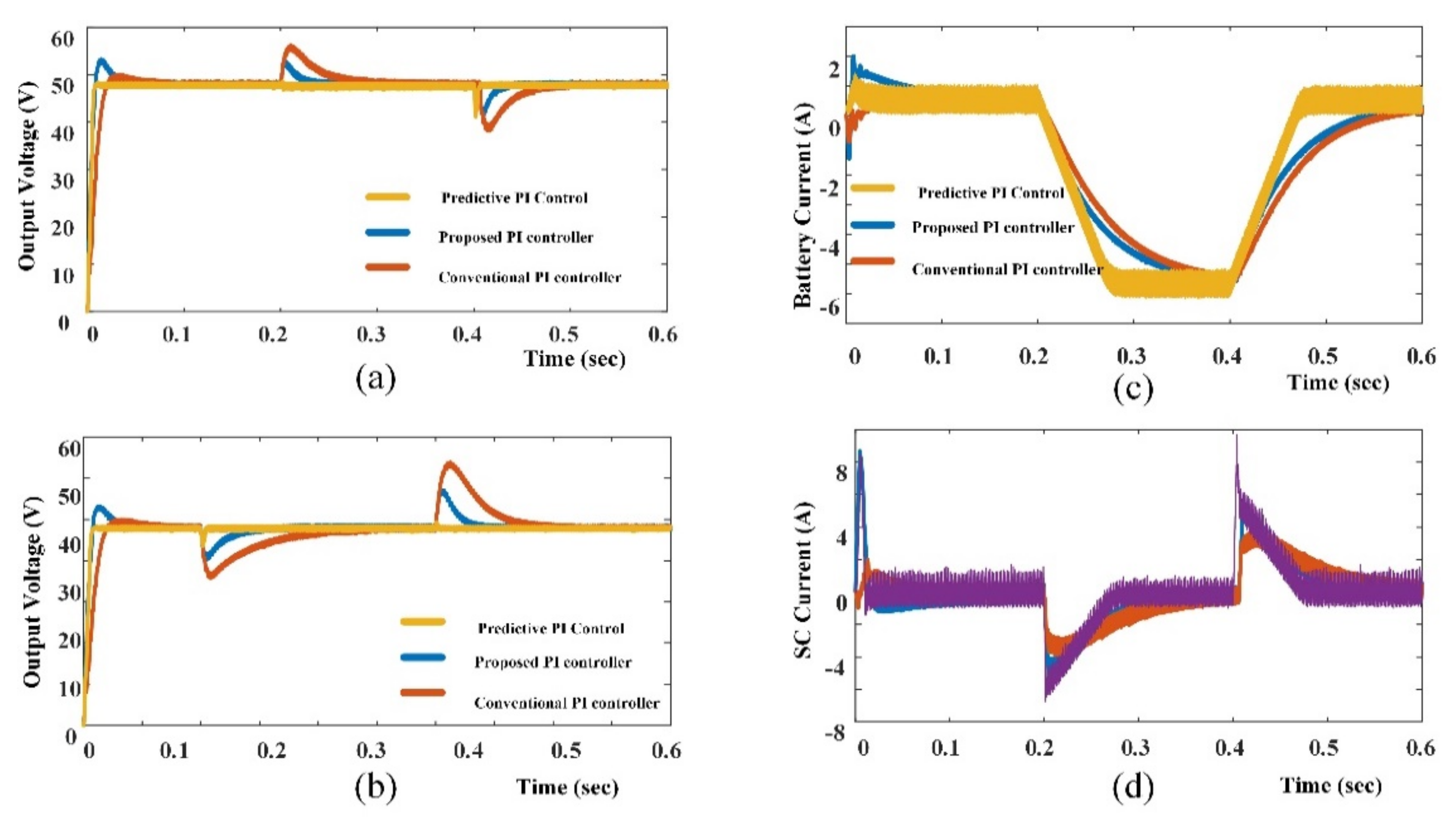
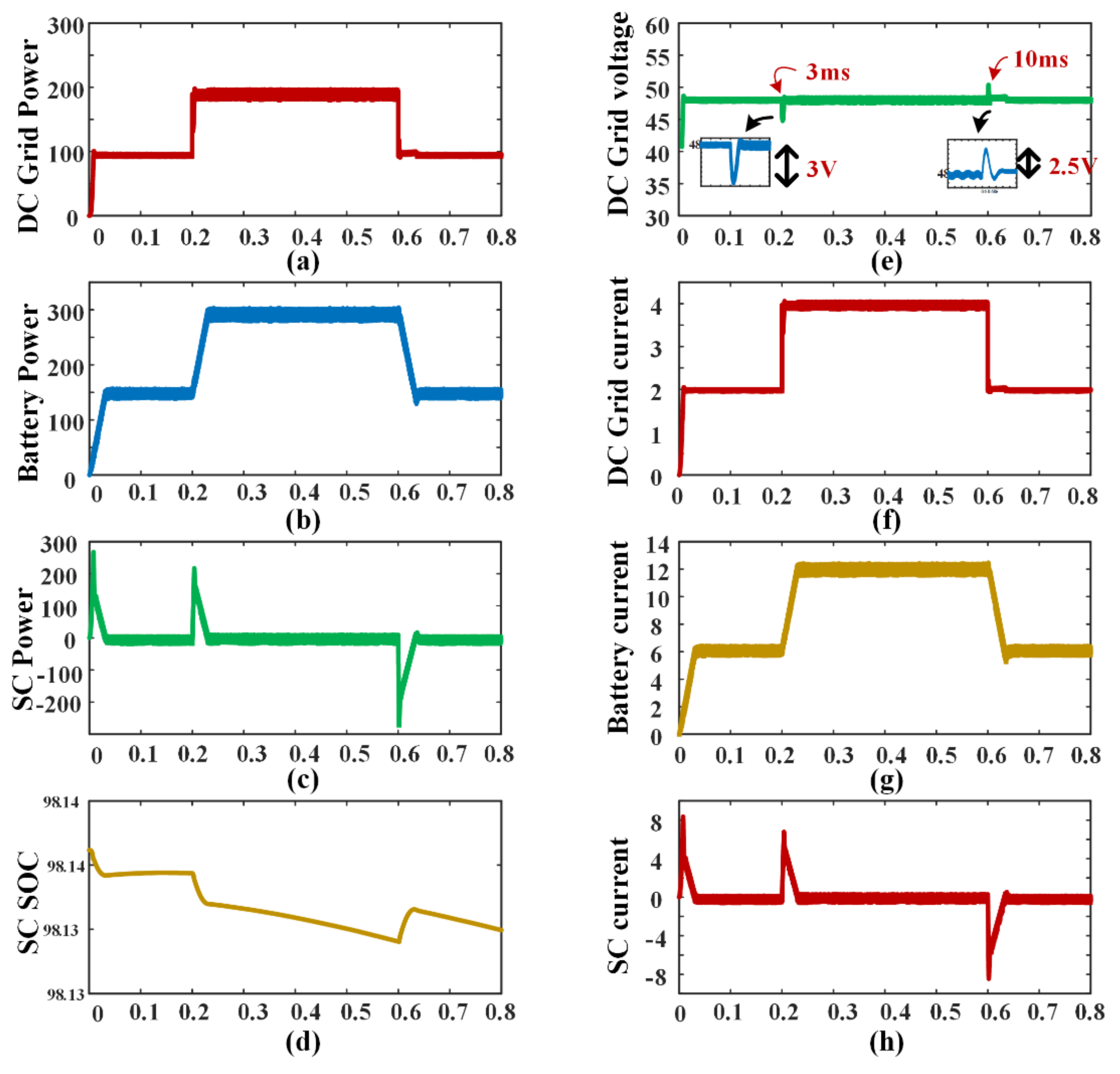
The DC grid voltage profile can be significantly improved in terms of settling time and maximum peak overshoot when using the predictive PI control compared to the proposed and traditional PI control methods.
The organization of the paper is as follows: Operation of bidirectional DC-DC converters with two inputs are addressed in Section 2. The conventional, proposed, and predictive PI control schemes are examined in Section 3 [39]. State-of-Charge Controller for Supercapacitors controller is discussed in Section 4. Simulation results with three controllers are discussed in Section 5. The experimental validation is discussed in Section 6. The research findings and interpretations are wrapped up in Section 7.

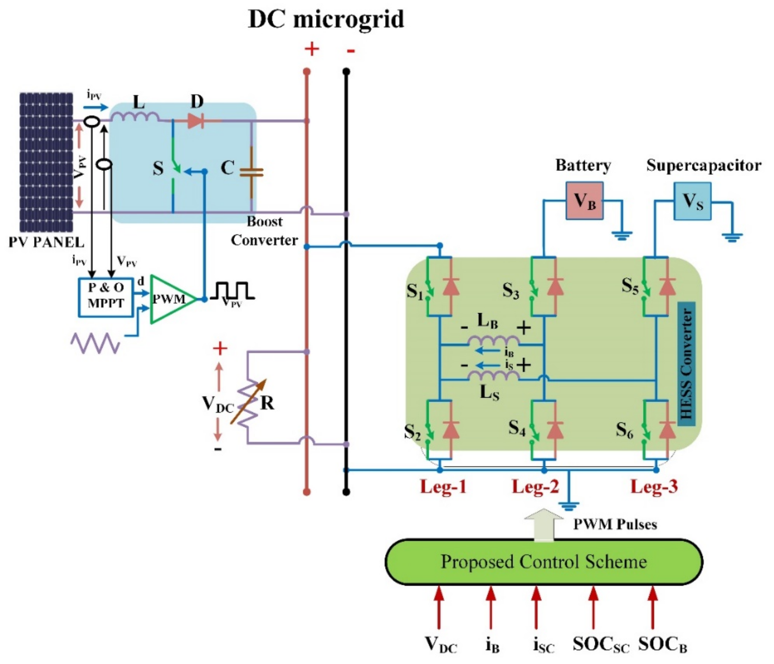
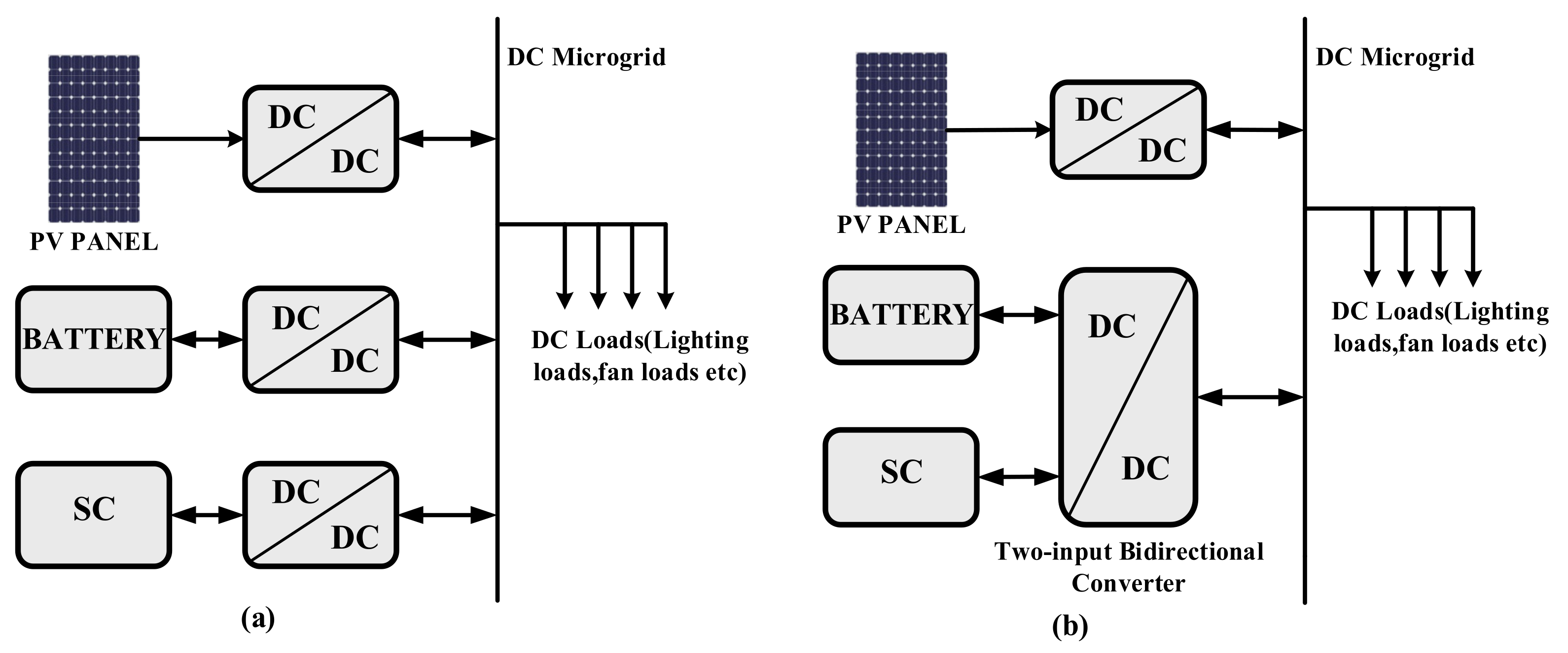
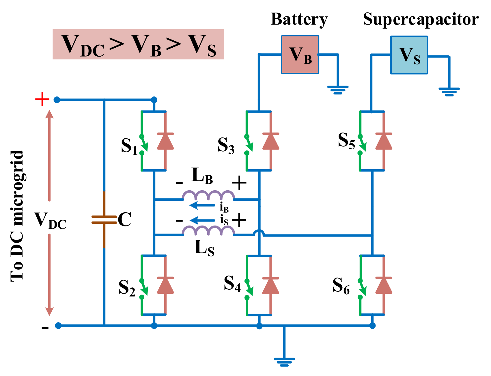
2. Operation of a Bidirectional DC-DC Converter with Dual Inputs

Figure 3 depicts a bidirectional converter with two inputs [39] and goes into great depth about the various modalities of operation. The converter’s modified operation is described here. It is made up of three switch legs. Legs 2 and 3 are connected to the battery voltage (VB) and supercapacitor voltage (VS) modules, respectively, while Leg 1 is connected to a DC Microgrid voltage (VDC). In this converter topology, the voltage across the battery is lower than the DC grid voltage but higher than the supercapacitor voltage. The inductors LB and LS with High-frequency connect legs 1, 2, and 3 together. The following sections describe the various modes of operation.

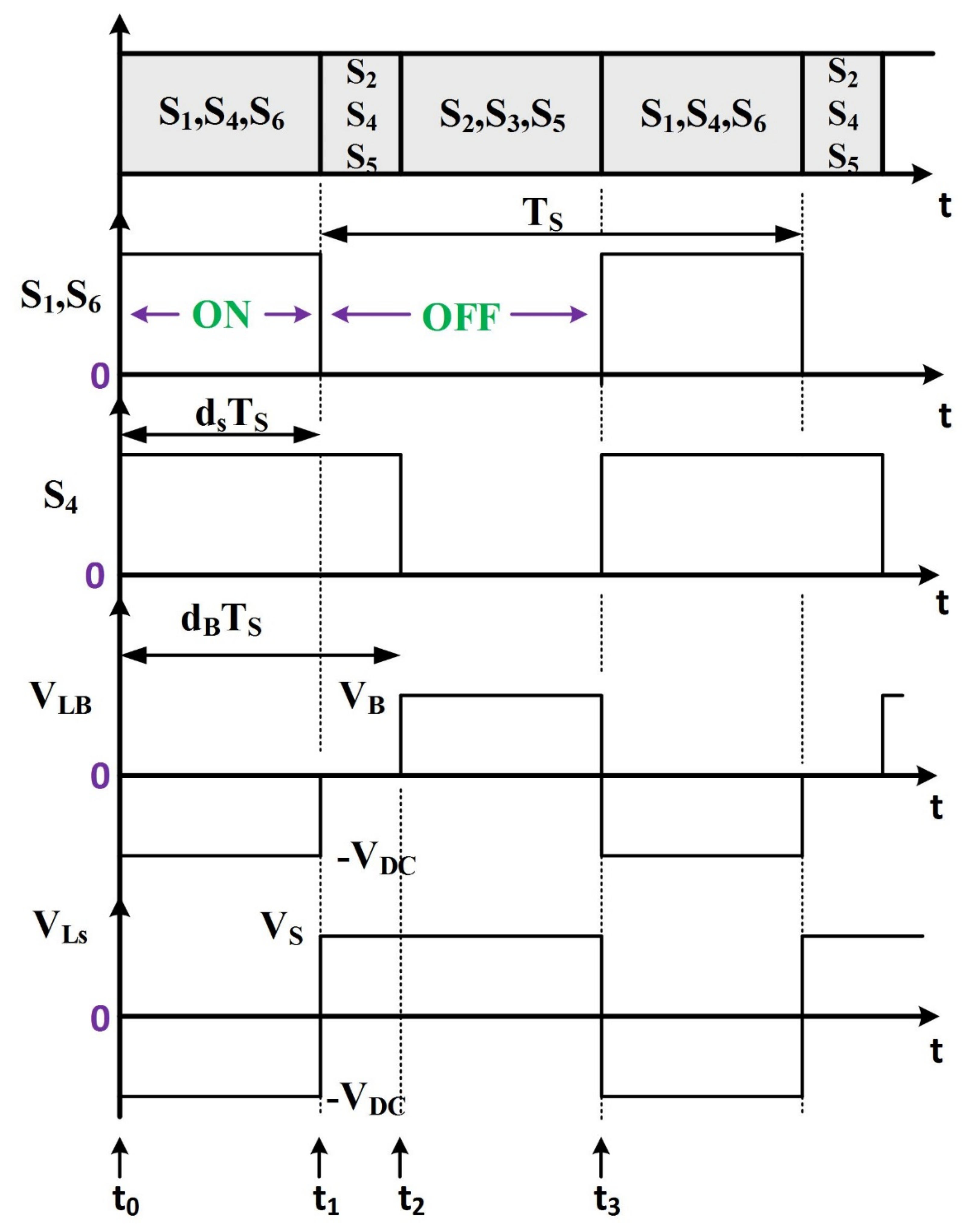
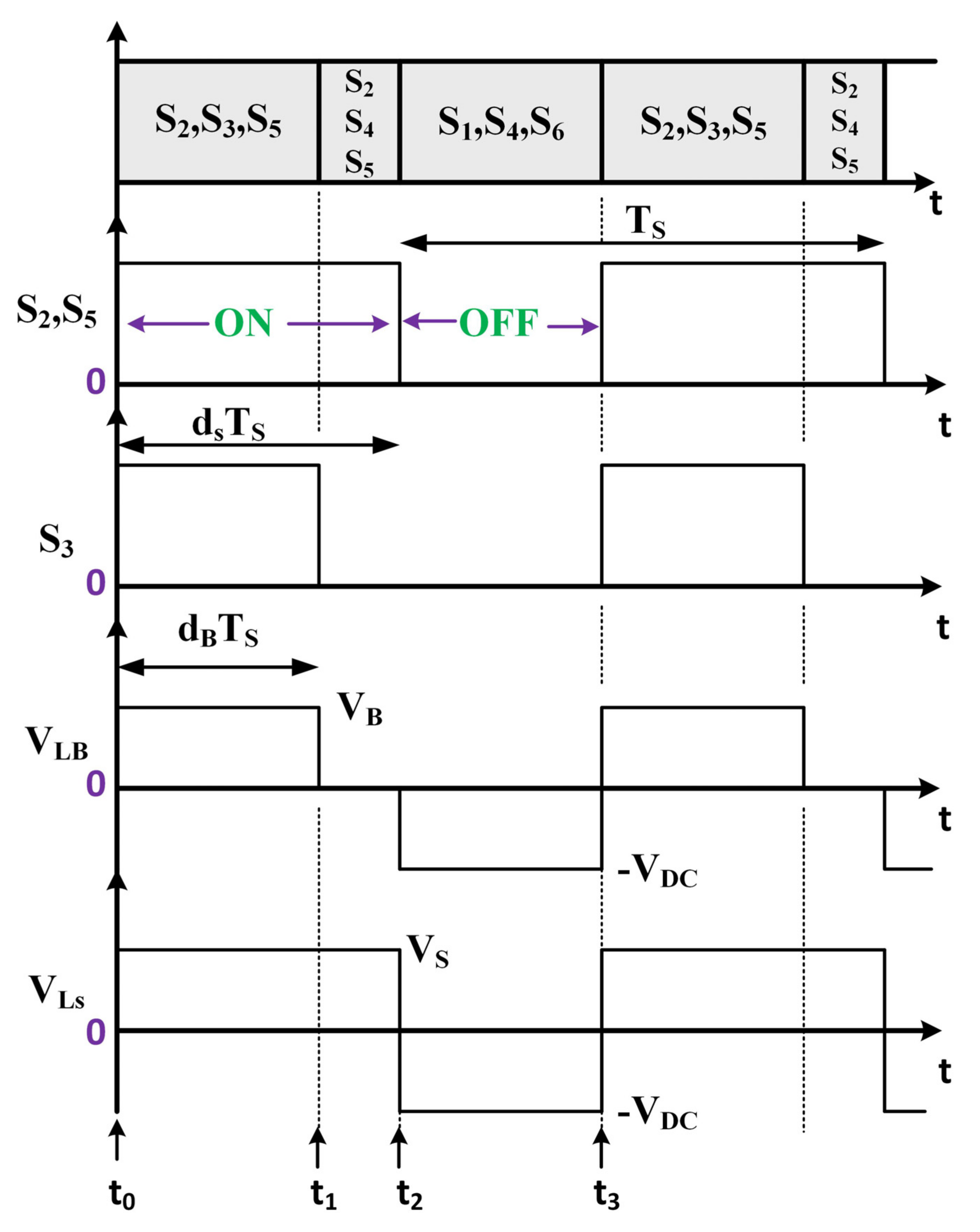
2.1. Discharging Sequence of HESS

The voltage in a DC Microgrid fluctuates significantly from the steady-state value while there may be a discrepancy between PV output and load power. When the demand exceeds PV generation capability or when PV-generated power is reduced owing to lower solar irradiation, DC Microgrid voltage drops. During this time, the HESS should give adequate power. In this mode of operation, power streams from the HESS to the DC Microgrid through the bidirectional converter are appropriately controlled.
The operation of the converter can be segregated into three time intervals, as shown in Figure 4. S1/S2, S3/S4, and S5/S6 are all switch pairs that work in tandem. In this mode, the switch pairs S2/S5 and S1/S6 always switch together, with complementary gating pulses. Switches S2, S3, and S5 are turned on at time instant t0, causing inductor currents iB and iS to grow linearly with slopes VB/LB and VS/LS, respectively. At t1, switch S3 is turned off, allowing current iB to flow freely through the S4 body diode. Switch S4 is turned on after a dead time interval for the switch pair S3/S4. S4 comes on with ZVS because its body diode is already conducting at the time the gating signal is sent. At t2, switches S2 and S5 are disabled, forcing inductor current iL2 to flow through the body diodes of switches S1 and S6 with a negative VDC/LS slope. With a negative slope of VDC/LB, inductor current iB flows via S1 body diode. Switch pairs S2/S1 and S5/S6 are gated on after the dead time intervals of switch pairs S2/S1. Because the body diodes of the corresponding switches are already in conduction, switches S1 and S6 are likewise turned on using ZVS, just as S4. S1, S4, and S6 are turned off at t3.
As a result, the body diodes of switches S2, S3, and S5 will conduct in order to keep the inductor currents flowing. Currents iB and iS flow with VB/LB and VS/LS positive slopes, respectively. Gating pulses are sent to switches S2, S3, and S5, which turn on with ZVS after a dead time gap. Applying a volt-second balance to the inductors LS and LB give results when dB is the duty cycle of the triggering pulse given to switch S3 and dS is the duty cycle of the triggering pulse delivered to switches S2 and S5.
V D C = d S 1 d S   .   V S
V D C = d B 1 d S   .   V B
d B will always be smaller than d S because VB is bigger than V S . As a result, the flow of power from the battery and supercapacitor to the DC Microgrid can be controlled individually by controlling dB and d S .

2.2. Charging Sequence of the HESS

Excess power appears to exist in the DC Microgrid when solar PV-generated power outweighs that required by the load, or when the load drops, resulting in an increase in DC Microgrid voltage. The battery and supercapacitor will be charged with extra power. As a result, electricity is transferred from the DC Microgrid to the HESS in this mode. As illustrated in Figure 5, the converter that operates in this mode can be segregated into three time intervals. S1 and S6 switch pairs are switched at the same time. S2 and S5 switch pairs are also gated at the same time, but with pulses that are complementary to S1 and S6. Switches S4 and S3 are also gated in a complementary manner. At t0, S1, S4, and S6 switches are activated causing the inductor currents iB and iS to decrease linearly in a negative direction with slopes VDC/LB and VDC/LS, respectively.
Until instant t1, the LB and LS inductors store energy during this period. At t1, the switch pair S1/S6 was turned off. The body diodes of switches S2 and S5 are turned on to maintain the inductor current is. The supercapacitor is now charged using the energy stored in the inductor LS. Through the body diode of switch S2, the inductor current iB freely circulates. Because the body diodes of the corresponding switches are already in conduction after a dead time interval for switch pairs S1/S6 and S2/S5, gating pulses are provided to S2 and S5, turning them on with ZVS. At time instant t2, switch S4 is turned off. Inductor current iS increases almost linearly with slope VS/LS through the body diode of switch S3. After the switch pair S4/S3 has reached its dead time interval, a gating pulse is triggered to S3 to turn it on with ZVS. The collected and stored energy in the inductor LB is now applied to charge the battery. Switches S2, S3, and S5 are turned off at instant t3, causing the body diodes of switches S1, S4, and S6 to turn on in order to keep the inductor currents flowing. To turn S1, S4, and S6 on with ZVS, triggering pulses are applied after dead time intervals. Applying a volt-second balance equation to the inductors LS and LB lead-in, if dS is the duty cycle of the gating pulse to the S1/S6 switch pair and dB is the duty cycle of the triggering pulse to switch S4.
V S = d S 1 d S   .   V D C
V B = d S 1 d B   .   V D C

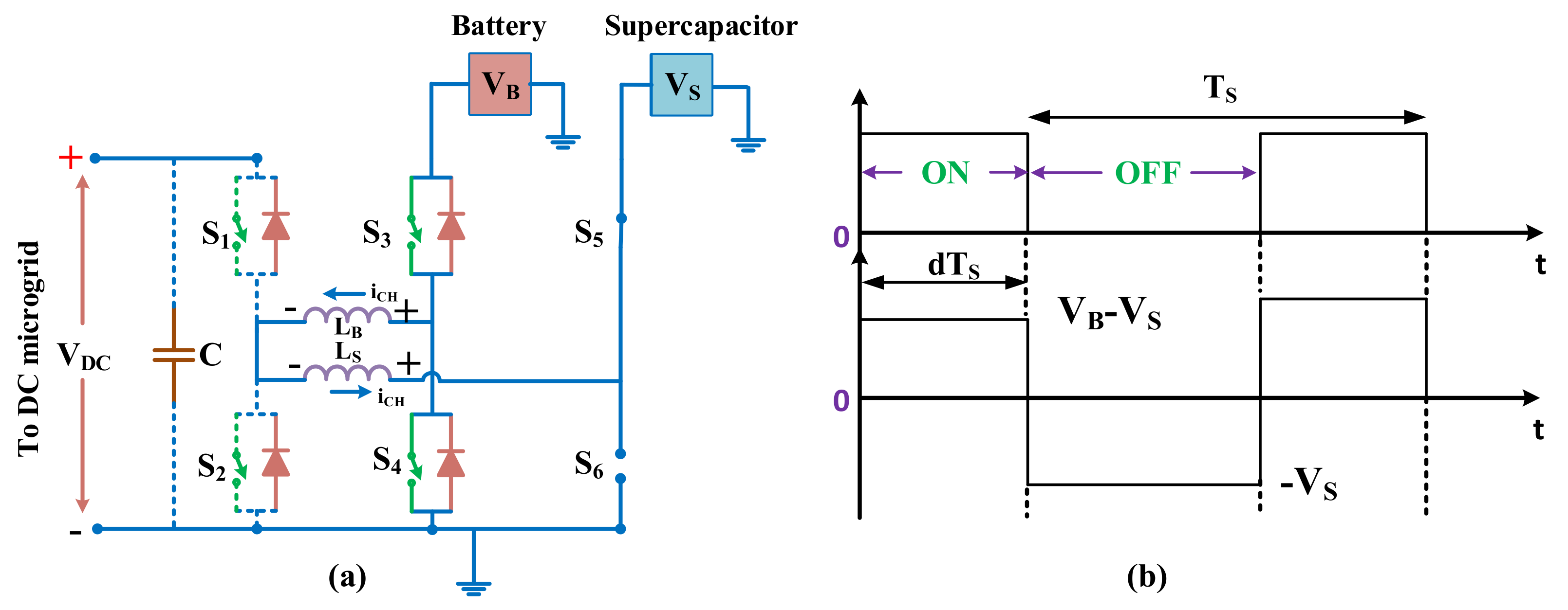
2.3. HESS Mode of Energy Exchange

A power density unit in a HESS is a supercapacitor. Due to its rapid self-discharging effect, it cannot offer energy for lengthy periods of time as a battery. To perform successfully in DC Microgrid applications with a HESS, the component ESSs must have sufficient energy stored in them. The supercapacitor must be charged from the battery energy density unit whenever necessary for the HESS to function effectively in order to keep its charge within acceptable limits. The path of power flow from the battery to the supercapacitor is represented by this mode. Figure 6 depicts the circuit topology for this mode (a).
In this mode of operation, the first switch leg (switches S1 and S2) is inactive, substantially isolating the DC Microgrid from the HESS while supercapacitor charging. S5/S6 switch pairs and S3/S4 switch pairs complement. In this mode, switch S5 is always turned on, causing switch S6 to be turned off. The duty cycle d is applied to switch S3. Figure 6 depicts the waveforms (b). Switch S3 controls the power stream from the battery to the supercapacitor, with the current ripple greatly decreased by connecting the inductors LB and LS in series. The user can adjust the power flow from the battery to the supercapacitor by using the d parameter. When the volt-second balanced equivalent series inductor L (L = LB + LS) is used, the result is:
V S = d   .   V B
In addition, the complementary action of switch S3 allows power to flow from supercapacitor to battery. Switch S4 is in boost mode, as indicated by this action. The procedure is similar to the one described previously.

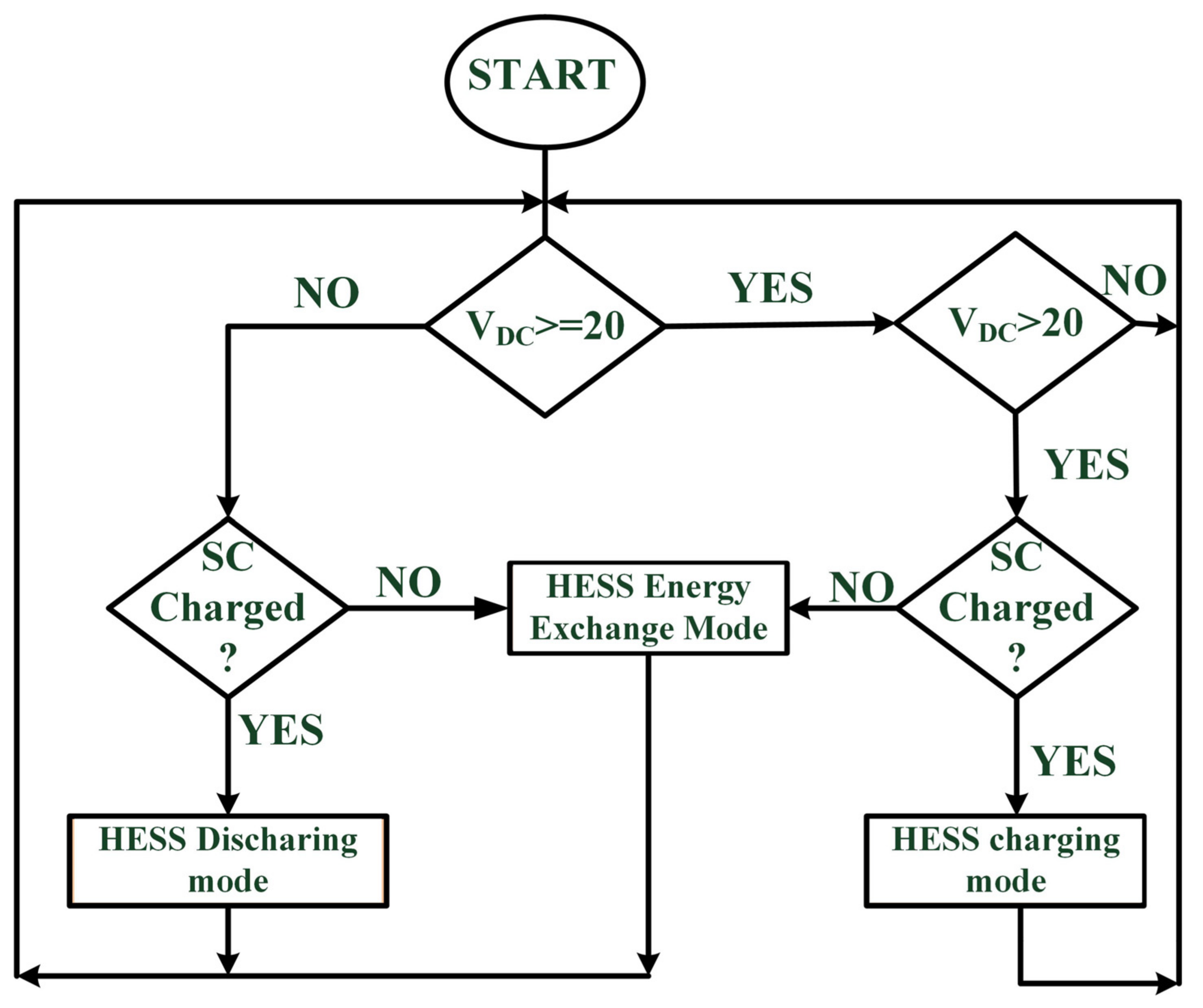
2.4. Transitions between Modes

The mode of operation is controlled from the existing state of the DC Microgrid and continuous SoC of supercapacitor monitoring. SoC of the Battery is not taken into account in this work because it is expected that battery energy is not lost as quickly as supercapacitor energy. Figure 7 shows a flow chart transition between distinct modes. The HESS enters charging mode when the DC Microgrid voltage exceeds the set reference, as long as the supercapacitor SoC remains within prescribed limits. The HESS will enter the charging operation mode when the DC Microgrid voltage falls below the predefined reference value, as long as the SoC of the supercapacitor is within the safety limit. The HESS enters energy exchange mode if the supercapacitor SoC exceeds the predefined limitations, electrically separating the DC Microgrid from the HESS. The working range of a supercapacitor SoC is described, as well as its mathematical formulation using Coulomb’s counting approach.
S O C M I N S O C S O C M A X
%   S O C = S O C i + 1 Q S C i C H d t × 100
where SoCi is the supercapacitor’s initial state of charge, QSC is the rated charge for the supercapacitor, and iCH is the charging current of the supercapacitor.

3. Double-Input Bidirectional Converter and Controller Design Using a Small Signal Linear Averaged Model

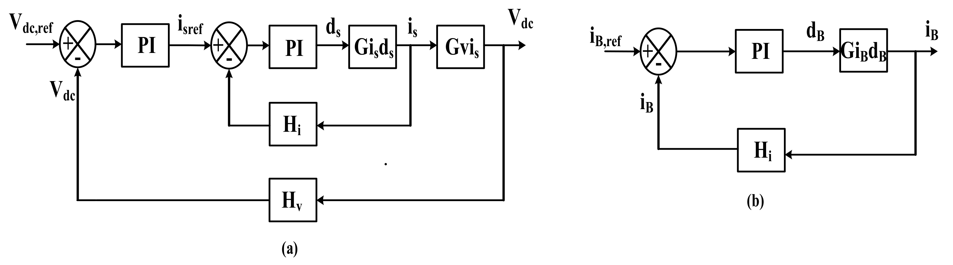
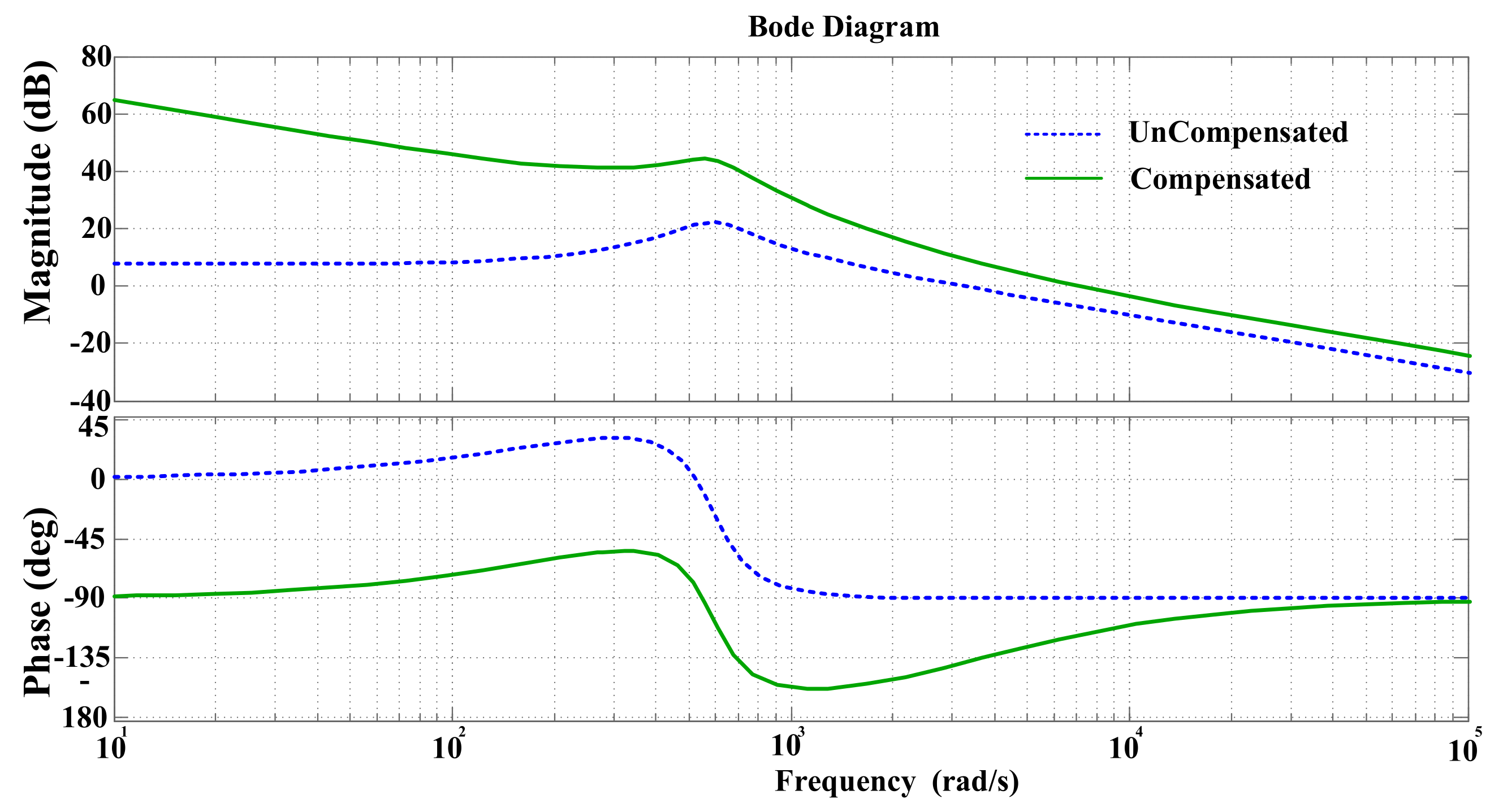
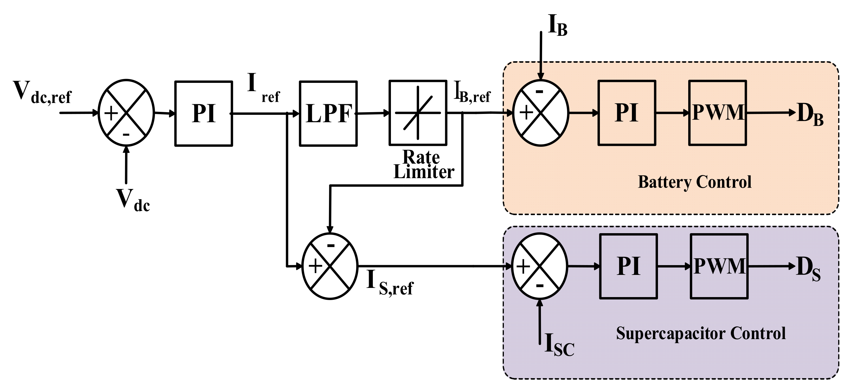
3.1. Design of Conventional and Proposed PI Control Scheme

The control system block diagram representation of the conventional PI and the proposed PI control schemes are shown in Figure 8 and Figure 9, respectively. The proposed control scheme will contribute a controller which will not only provide improved closed-loop performance but also provide stable operation amidst converter dynamics and external disturbances. The nominal value of DC link voltage (VDC) is compared with a reference voltage (VDC,ref) and the error is offered to the PI controller in both schemes, which generates total current (itot) from ESS in this process. In the conventional control scheme, total current is divided into low-frequency (ILOW) and high-frequency (IHIGH) components of current using a low pass filter, which is given as reference currents to battery and supercapacitor loops, respectively, and is represented in Figure 8. In the conventional control scheme, SC current reference consists of a high-frequency component and battery error component which is explained in the proposed control scheme. The conventional control scheme neglects battery current errors arising due to the battery controller.
The proposed control scheme is represented in Figure 9. The power flow in the DC grid under PV generation and load changes are classified into two types (i) steady-state power component (Pstd), and (ii) transient power component (Ptran). The power balance equation is given as
Pdc(t) − Pren(t) = PB(t) + PSC(t) = Pstd(t) + Ptran(t)
where, Pdc(t), Pren(t), PB(t) and PSC(t) are the DC grid power, RES power, battery, and SC power respectively. The HESS charges and discharges, maintaining the DC grid voltage within predefined limits. The sum of battery and SC powers are given as
PB(t) + PSC(t) = Pstd(t) + Ptran(t) = VDC.itot(t)
Regulates the DC link voltage by controlling total current demand represented as follows
i t o t = P s t d ( t ) + P t r a n ( t ) V D C ( t )   = i s t d ( t ) + i t r a n ( t )
The voltage control loop calculates the total current i t o t demand as follows:
i t o t ( t ) = i s t d ( t ) + i t r a n ( t ) + K p v . v e r r + K i , v . v e r r . d t
where Kp,v and Ki,v are the proportional and integral constants of the outer voltage control loop, respectively, and verr represents voltage error. Better DC bus voltage regulation is achieved by effective sharing of total current demand ( i t o t ). In a conventional control scheme, a low pass filter (LPF) extracts the steady-state component from the total current ( i t o t ).
i B , r e f ( S ) = i s t d ( s ) = w C S + w C   .   i t o t ( s )
where w C represents LPF cut-off frequency and i B , r e f ( S ) represents the battery current reference for the battery control loop. Steady-state current is controlled by a battery system. Due to the slow response of the battery system, uncompensated power is observed from the battery system. The battery uncompensated power is given as follows:
P B _ u n ( S ) = ( i B , r e f ( s ) i B ( s ) ) . v B ( s )
P B _ u n ( S ) = i B , e r r ( S ) . V B ( s )
where P B _ u n ( S ) is the uncompensated power from the battery system. In the proposed control strategy, uncompensated power is utilized to improve the performance of the SC. Utilizing both uncompensated power and the transient current component to design a new SC reference current is given as follows:
i t r a n ( s ) = ( 1 w C S + w C ) . i t o t ( S )
i S C , r e f ( s ) = i t r a n ( S ) + ( i B , r e f ( S ) i B ( S ) ) . V B ( S ) V S C ( S )
The battery and SC reference currents are compared with actual currents. Battery and SC error current are fed to the PI controller. The duty cycle is calculated for the respective current references, where dB and dSC are the duty cycle for battery control and SC control, as shown in Figure 10.
The circuits described in the previous section can be used to independently control the flow of power from the battery and supercapacitors to the DC Microgrid. As a result, it is possible to build a separate small-signal model of the battery and supercapacitor stages, similar to building a dynamic model of two single-input bidirectional converters. With the availability of multi-input, multi-output control systems [24], this isolated averaged battery and supercapacitor power flow stage small-signal model facilitates the design of simpler control systems. The battery-to-DC Microgrid and supercapacitor-to-DC Microgrid small-signal models are configured as follows:
Due to the complimentary operation of the switch, an integrated controller for charging and discharging the battery/supercapacitor is sufficient, even though both circuit activities share the same small-signal transfer function. The HESS discharge mode is taken into account when creating the linear model. Due to the inevitable supercapacitor’s intrinsic fast dynamic responsiveness, the outer voltage loop is designed around it.
A current in the inner loop and a voltage in the outer loop make up the control system for a supercapacitor stage, as shown in Figure 10a. A current controller, as shown in Figure 10, controls the battery current reference (b). In order to give a faster reaction, a supercapacitor’s inner current loop is constructed with greater bandwidth than that of a battery. The inner current loop runs at a quicker rate than that of the outer voltage loop. The bandwidth in a voltage loop is smaller than the current in an inner loop. The switching frequency that is evaluated is 10 kHz.

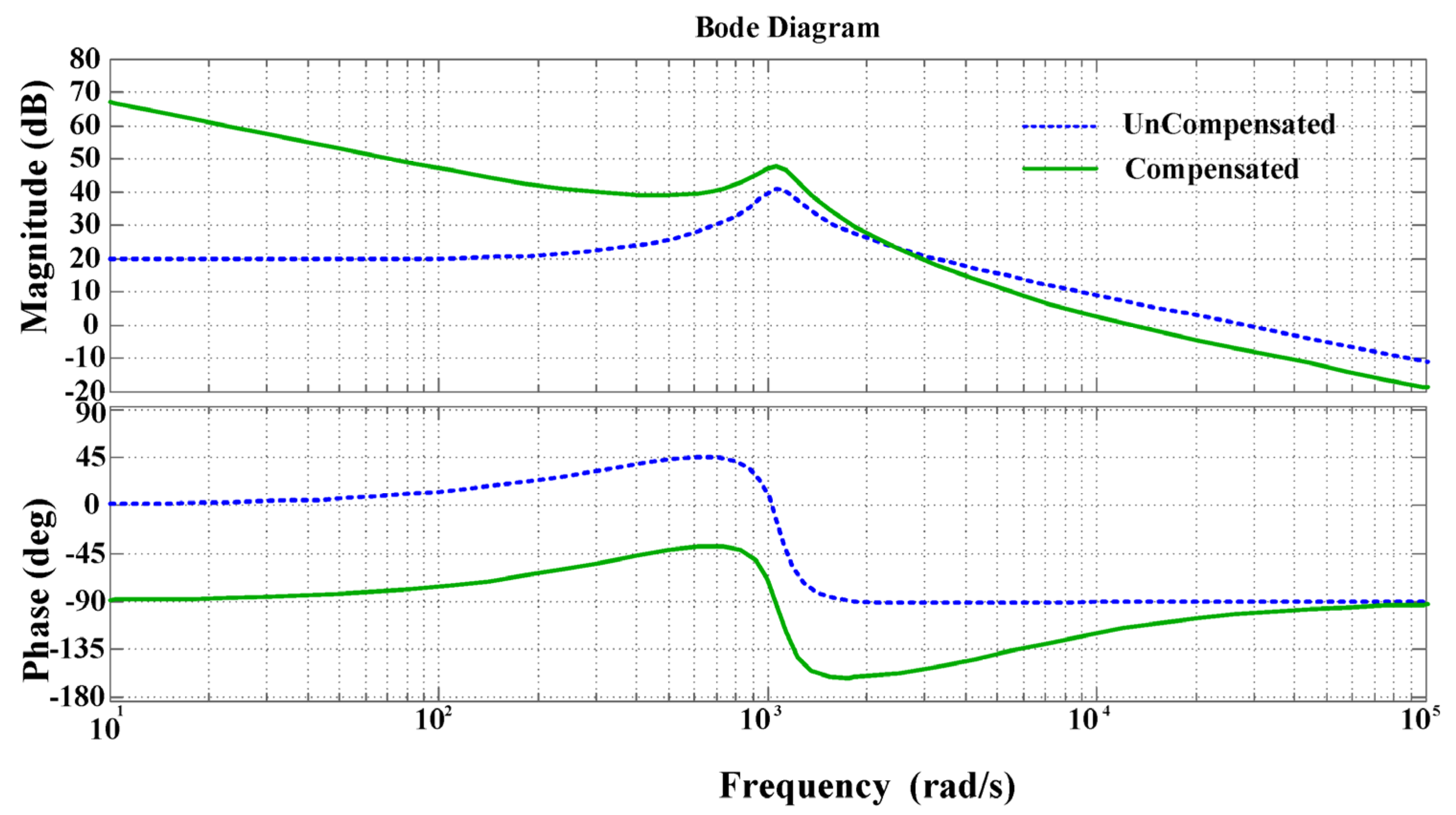
3.1.1. The Supercapacitor-DC Microgrid Stage Small Signal Linear Averaged Model

The state equations throughout time interval (t0~t2) can be framed as shown in Figure 4 and as discussed in Section 3.
L S d i L S d t = v S C C d v D C d t = v D C R
In the time interval (t2~t3), the state equations can be framed as:
L S d i L S d t = v D C C d v D C d t = i L S v D C R
The preceding state equations are perturbed and linearized to provide small-signal transfer functions with the control-to-inductor current and inductor current-to-voltage.
G i S C d S C = i S C ( s ) d S C ( s ) = V D C ( 1 + D S C ) R ( 1 D S C ) 3 1 + s R C 1 + D S C s 2 L S C C 1 D S C 2 + s L S C R 1 D S C 2 + 1 G v D C i S C = v D C ( s ) i S C ( s ) = R ( 1 D S C ) ( 1 + D S C ) 1 s D S C L S C R ( 1 D S C ) 2 1 + s R C 1 + D S C
A PI controller for the inner current loop is constructed with a bandwidth of 1.6 kHz and a phase margin of 60°. Figure 11 depicts a Bode plot of adjusted and uncompensated transfer functions. The function of transfer is defined as follows:
G p i _ i S = 0.4124 + 2291 s
The averaged model is used to develop the PI controller for the outer voltage loop. The bandwidth must be lesser than half-plane zero on the right side. With a bandwidth of 200 Hz and a phase margin of 60°, the voltage controller is constructed. Figure 12 depicts a Bode plot for the same scenario. The function of transfer is defined as follows:
G p i _ v = 0.5054 + 266 s

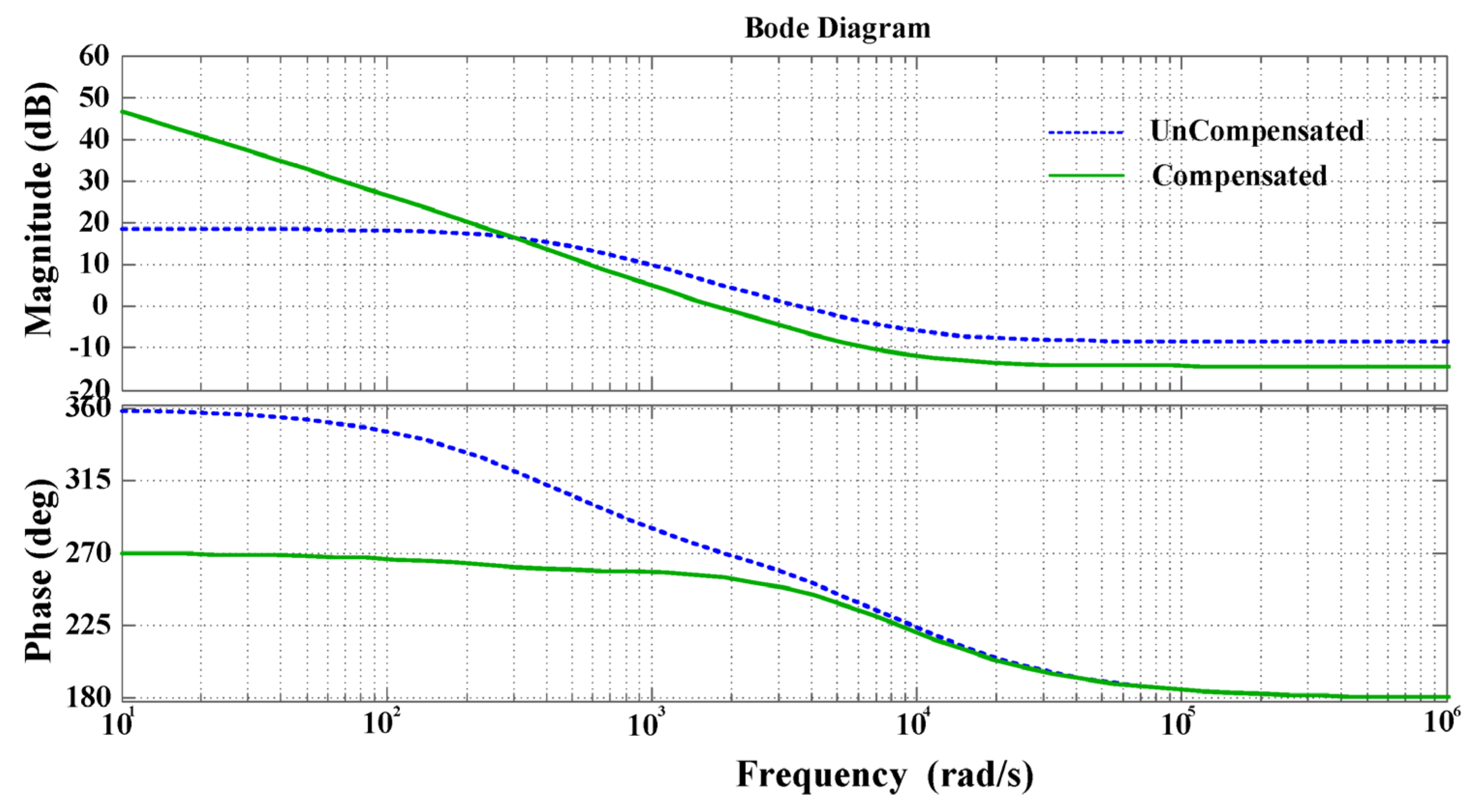
3.1.2. Modeling a Battery-DC Microgrid Stage with a Small-Signal Linear Averaged Model

As illustrated in Figure 4, the discharge process in the battery is accomplished in three time periods. The state equations for the time interval (t0~t1) are as follows, as discussed in Section 3.
L B d i B d t = v B C d v D C d t = v D C R
After translating into the frequency domain, the equations of the state can be framed in matrix form as follows:
d X d t = A X + B U Y = C X + E U
where X is a matrix consisting of all state variables (iB, VDC), U is a matrix consisting of inputs, and Y is a matrix consisting of all the system outputs. It can be rewritten in matrix form as:
d i B d t d v D C d t = A 1 i B v D C + B 1 v D C i B = C 1 i B v D C + E 1 v D C
where A 1 = 0 0 0 1 R C , B 1 = 1 L B 0 , C 1 = 1 0 , and E 1 = 0 .
Similarly, for the second time interval (t1~t2), in matrix form, the state equations and state model can be framed as follows:
L B d i B d t = 0 C d v D C d t = v D C R
d i B d t d v D C d t = A 2 i B v D C + B 2 v D C i B = C 2 i B v D C + E 2 v D C
where A 2 = 0 0 0 1 R C , B 2 = 0 0 , C 2 = 1 0 , and E 2 = 0 .
In the third time interval (t2~t3), in matrix form, the state equations and state model can be framed as follows:
L B d i B d t = v D C C d v D C d t = i B v D C R
d i B d t d v D C d t = A 3 i B v D C + B 3 v D C i B = C 3 i B v D C + E 3 v D C
where A 3 = 0 1 L B 1 C 1 R C , B 3 = 0 0 , C 3 = 1 0 , and E 3 = 0 .
The bidirectional converter will be confined to the state model represented by (24) for a time period of (dB ∙ TS), after which it will transition to the model represented by (26), where it will stay for a duration of [(dSdB) ∙ TS], as shown in Figure 4. For the designed model, the duration of the third time interval is [(1 − dS) ∙ TS] (28). As a result, the following is the converter’s averaged state model:
A = A 1 d B + A 2 ( d S d B ) + A 3 ( 1 d S ) B = B 1 d B + B 2 ( d S d B ) + B 3 ( 1 d S ) C = C 1 d B + C 2 ( d S d B ) + C 3 ( 1 d S ) E = E 1 d B + E 2 ( d S d B ) + E 3 ( 1 d S )
d x d t = A x + B u y = C x + E u
When state variables are perturbed about X’s steady-state DC value,
x = X + x ^
Assuming that (dB and dS) are duty cycles and both inputs are perturbed (u),
d S = D S + d ^ S d B = D B + d ^ B u = U + u ^
In comparison to steady-state DC values, the perturbations in the small-signal model should be very minimal. Furthermore, during a single switching time, these perturbations are intended to be constant. The converter’s state-space model is generated by substituting (30) and (31) into (29) and linearizing by ignoring second-order elements.
x ^ ˙ = d x ^ d t = A x ^ + B u ^ + F d ^ B + G d ^ S y ^ = C x ^ + ( C 1 C 2 ) X d ^ B + ( C 2 C 3 ) X d ^ S
where F = (A1A2)X + (B1B2)U, G = (A2A3)X + (B2B3)U, and X = −A−1BU. Applying Laplace transform to (32), the controlled output transfer function of the battery stage is reframed as:
y ^ ( s ) d ^ B ( s ) = C s I A 1 F + C 1 C 2 X
where I is the identity matrix. Substituting the values for C, A, F, C1, C2, and X from (29), (32), (24), and (26), the current transfer function from battery stage control to the inductor can be configured as follows:
G i B d B = i ^ B ( s ) d ^ B ( s ) = V D C D B R ( 1 D S ) 1 + s R C s 2 L B C ( 1 D S ) 2 + s L B R ( 1 D S ) 2 + 1
The above transfer function is used to design a PI controller for regulating battery current. The controller’s bandwidth is reduced to match that of the supercapacitor stage. The designed controller has a bandwidth of one kHz and a phase margin of 60°. Figure 13 depicts a bode plot of compensated and uncompensated plants. The PI controller’s transfer function is provided by:
G p i _ i B = 1.971 + 7300 s

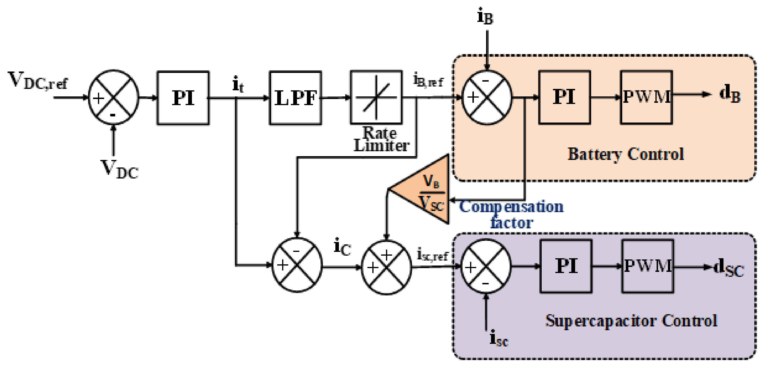
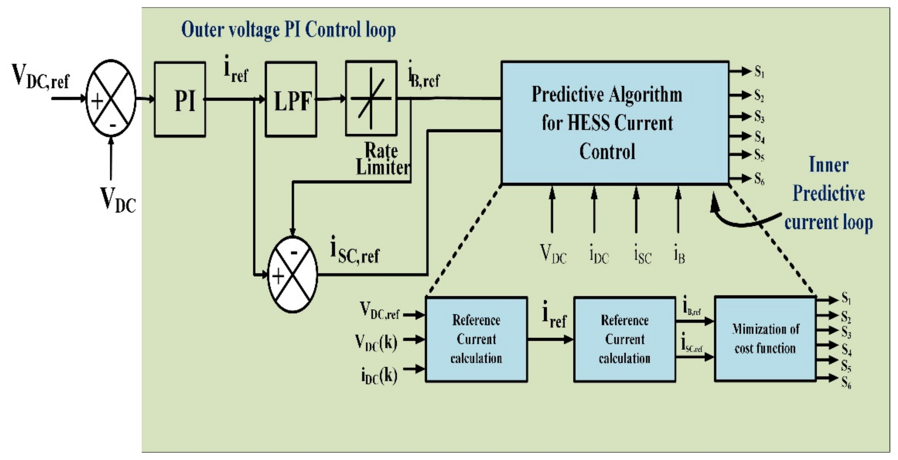
3.2. Predictive PI Control Scheme

The block diagram representation of the predictive PI control scheme for a HESS is shown in Figure 14. To control the battery and SC currents simple, a predictive PI control scheme algorithm is implemented. The charging and discharging mode of operation depends on PWM pulses applied to the switches. The boost mode of operation is discussed for the battery and SC system.

Inner Predictive PI Control Scheme

For the prediction of battery and SC inductor currents an averaged voltage balance equation across these inductors is developed, for L b
L b d i b d t = V b d b V d c ( 1 d b )
By using Euler’s difference law
L b i b ( k + 1 ) i b ( k ) T S = V b ( k ) d b ( k ) V d c ( k ) ( 1 d b ( i ) )
The above equation i b ( k + 1 ) is calculated:
i b ( k + 1 ) = T s L b . [ V b ( k ) d b ( i ) V d c ( k ) ] + i b ( k )
Similarly, the SC inductor current model is derived as follows
L S C d i S C d t = V S C d S C V d c ( 1 d S C )
From the above equation i S C ( k + 1 ) is derived as
i S C ( k + 1 ) = T S L S C . [ V S C ( k ) d S C ( i ) V d c ( k ) ( 1 d b ( i ) ) ] + i S C ( k )
The cost functions for battery and SC current control are
J b = ( ( i b , r e f i b ( k + 1 ) ) 2
J S C = ( ( i S C , r e f i S C ( k + 1 ) ) 2
Using i b ( k + 1 ) and i S C ( k + 1 ) equations calculated iteratively for duty cycles d b and d S C from 0 to 1 with an increment of 0.01, each of these values compared with i b , r e f and i S C , r e f during every sampling interval and the duty cycle which gives the least cost function value was selected.

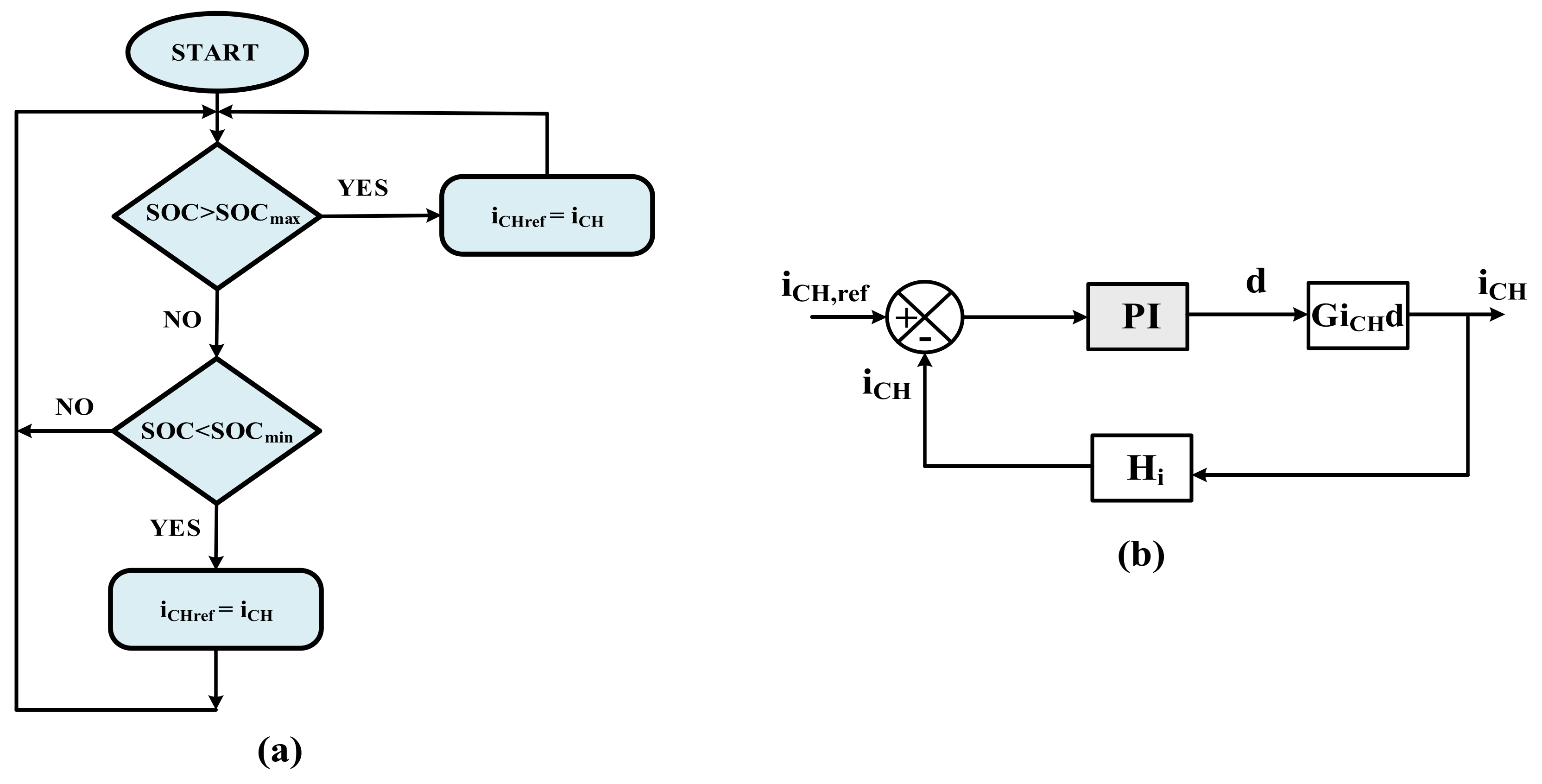
4. State-of-Charge Controller for Supercapacitors

Supercapacitors have a very low ESR compared to batteries. As a result, they are unable to store energy for a long time. The control logic is designed to keep the SoC within the appropriate limits of energy to avoid supercapacitor energy from being depleted beyond a minimum permitted level (6). Beyond this intended SoC range, the converter enters the HESS energy exchange mode specified in Section 3. When the supercapacitor’s SoC falls below the required minimum, it is charged using battery power at a constant current, ICH. When the SoC reaches the maximum safe zone, the supercapacitor is allowed to discharge its extra energy to the battery, allowing the battery to operate at a constant current ICH. As discussed in Section 3, either the buck (SC charging) or boost (SC discharging) operation keeps the supercapacitor’s SoC within acceptable ranges. The SoC controller’s control logic is illustrated in Figure 15. A PI controller regulates the supercapacitor current. The controller’s design is based on the buck mode control-to-output transfer function. It is worth noting that the DC Microgrid is electrically isolated from the HESS whenever the HESS Energy exchange mode is triggered, whether due to high or low SoC values.

5. Simulation Results and Analysis

This chapter shows the outcomes of two test cases using the proposed control systems. The nominal simulation research parameters are shown in Table 1. MATLAB Software is used to implement the entire model. Two bidirectional converters, one for the battery and one for the SC, make up the model. The PV array system is a one-way connection to a boost converter. The following sections outline the two operational scenarios for a step change in Solar PV generation and load demand.

5.1. Step Increase in PV Generation

The simulation results for step change in PV generation and conventional and proposed PI control schemes are shown in Figure 16 and Figure 17, respectively. In both control schemes, due to atmospheric variations, power produced by the PV panel increases from 96 W to 192 W at t = 0.3 s. Due to this PV, current increases from 3 A to 6 A at t = 0.3 s. In this case, the load power requirement is constant at 96 W. As PV power is more than the load power requirement, DC grid voltage increases more than 48 V. Immediately, SC absorbs excess power of 96 W for a short duration until the battery can regulate the grid voltage to 48 V. Thus, the battery and SC charge according to the energy management scheme to maintain the grid voltage at 48 V. The simulation shows a settling time of 100 ms for the conventional control scheme and 35 ms for the proposed PI control scheme. The proposed control scheme has better dynamic performance and fast DC grid voltage regulation due to the utilization of uncompensated power from the battery system to improve the SC system.

5.2. Step Decrease in PV Generation

Figure 16 and Figure 17 show the simulation results for a step decrease in PV generation for the conventional and proposed PI control schemes, respectively. In both control schemes, due to atmospheric variations, power produced by the PV panel changes from 96 W to 192 W at t = 0.6 s. The step decrease in PV generation causes a step decrease in PV current from 6 A to 3 A. The sudden decrease in PV generation causes a decrease in DC grid voltage. The settling time for the conventional and proposed PI schemes are 120 ms and 30 ms, respectively. The proposed control scheme is approximately four times faster compared to the conventional control scheme. From the results, it can be observed that the performance of the proposed scheme is better than the conventional control scheme.

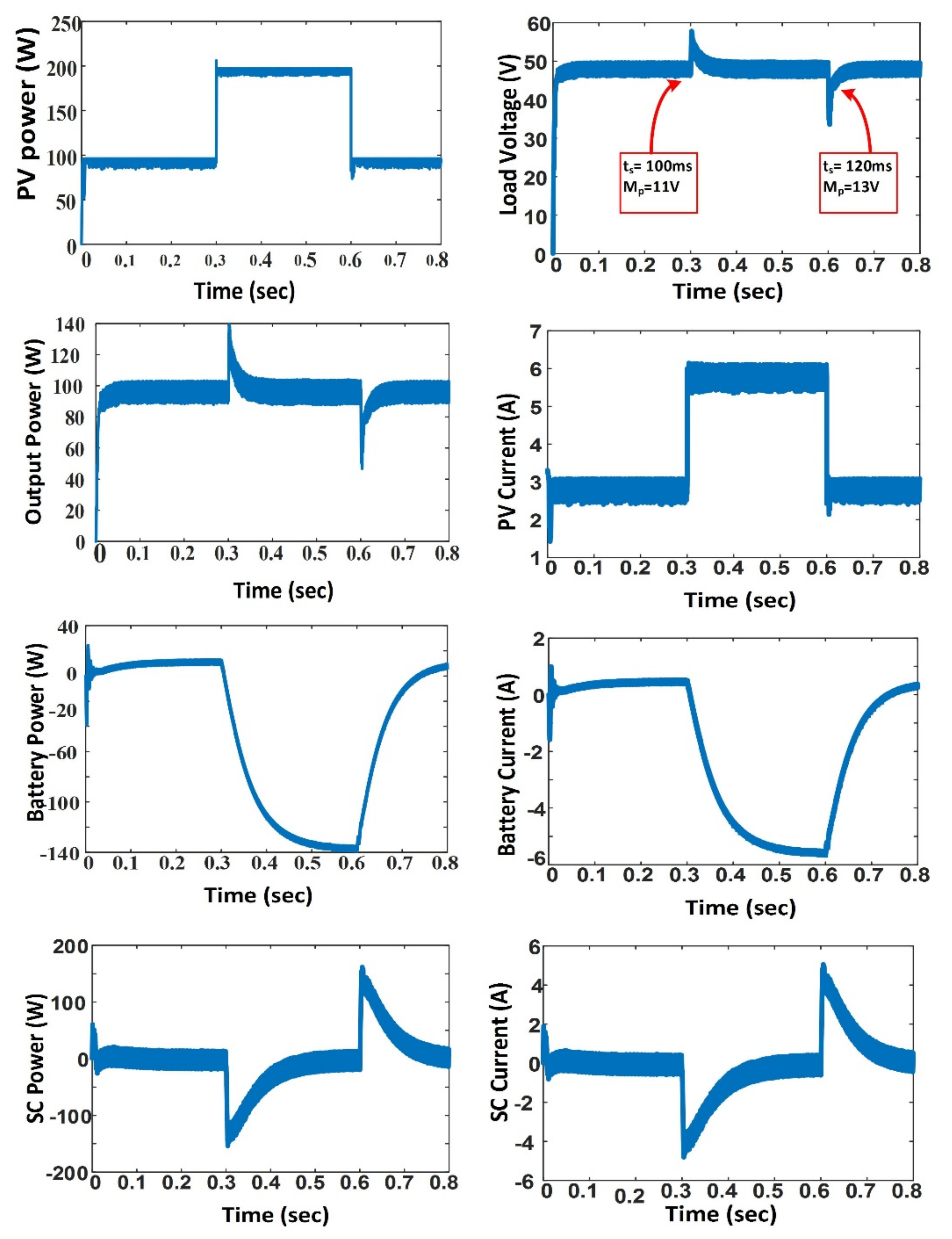
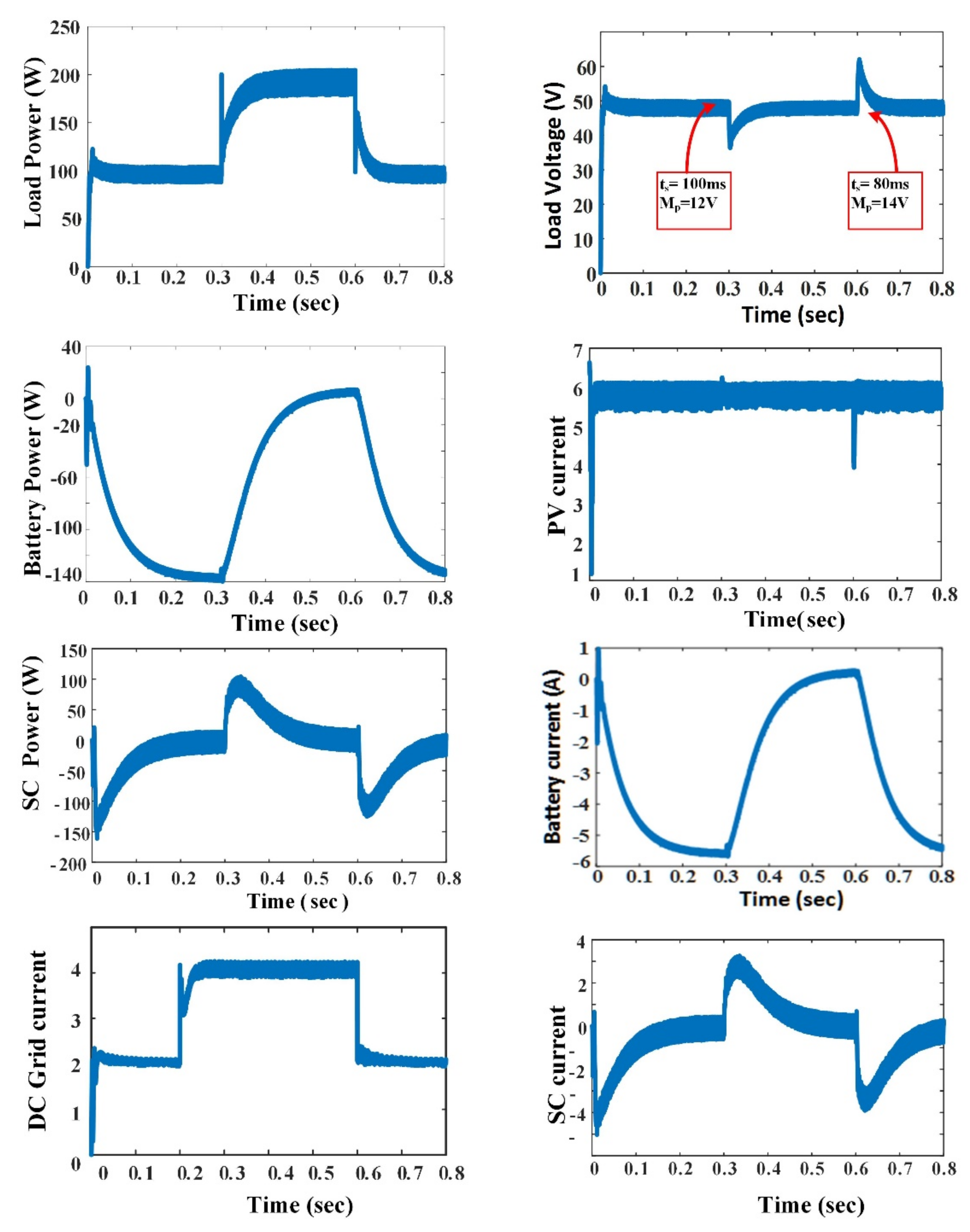
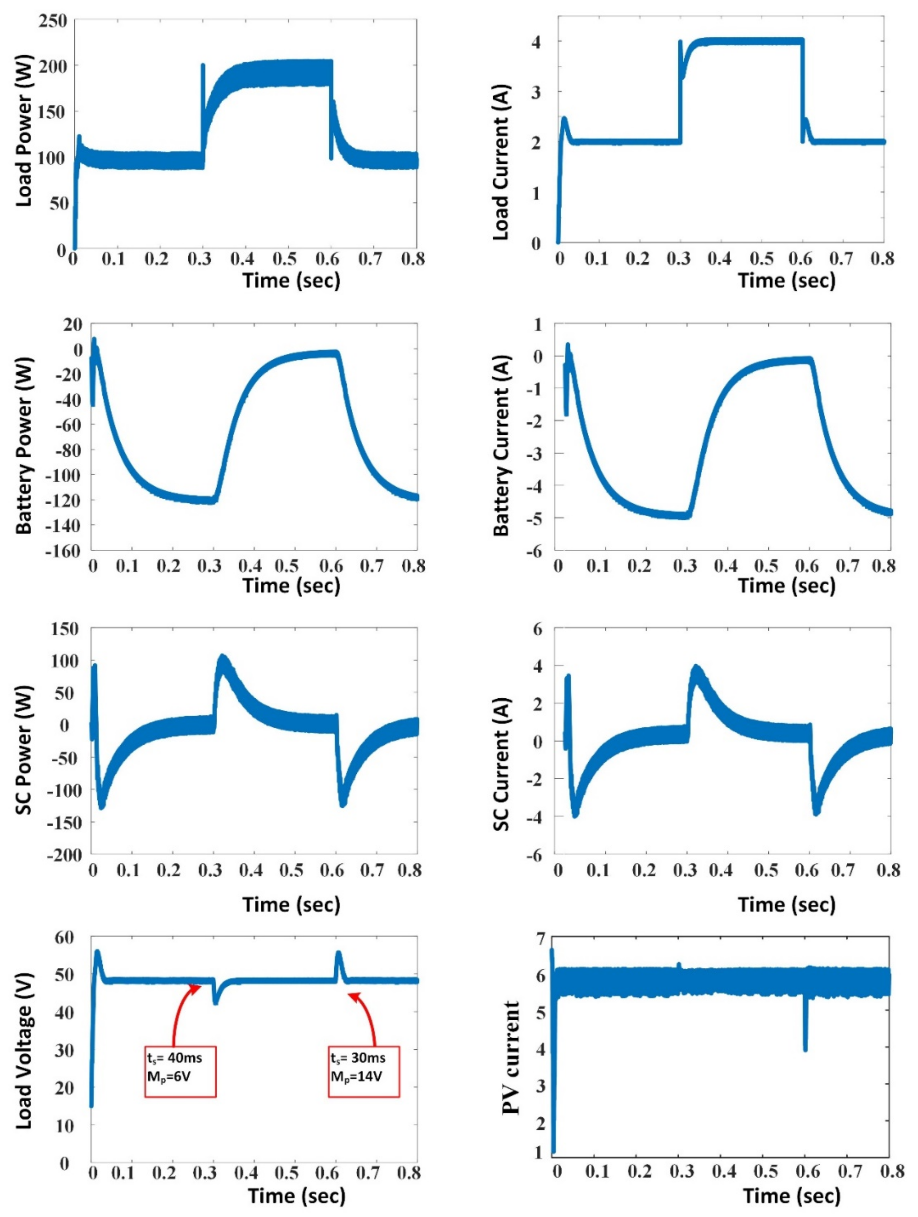
5.3. Step Increase in Load Demand

Figure 18 and Figure 19 show the Simulation results for a step increase in load demand for the conventional and proposed PI control schemes, respectively. At an instant t = 0.3 s, load demand increases from 96 W to 192 W. This increases the load current from 2 A to 4 A. During this time, the PV current is constant at 3 A. Before t = 0.3 s, the steady-state values were VDC = 48 V, iPV = 3 A, io = 2 A. At t = 0.3 s, the load demand increases to 192 W, which is beyond the power range of PV generation. This creates a power imbalance between source power and load power. The HESS immediately responds, SC supplies the transient component, and the battery supplies the steady-state component of power demand. The DC grid voltage is regulated at 100 ms in the conventional control scheme and 40 ms in the proposed control scheme.

5.4. Step Decrease in Load Demand

Figure 18 and Figure 19 show the simulation results for a step decrease in load demand for the conventional and proposed PI control schemes, respectively. At t = 0.6 s, load power demand decreases from 192 W to 96 W. This causes load current changes from 4 A to 2 A. The sudden change in load current affects the DC grid voltage. The HESS responds immediately to these fluctuations to handle the excess power in the DC Microgrid. The transient component of power handled is by the SC, while the average or steady-state component of power is handled by the battery in both the control schemes. The times taken to restore the voltage, in the conventional and proposed PI control schemes, are 80 ms and 30 ms, respectively. From the results, it can be seen that the proposed control scheme is faster with less peak overshoot DC Microgrid voltage compared to the conventional control scheme. The nominal parameters for simulation study as presented in Table 1.

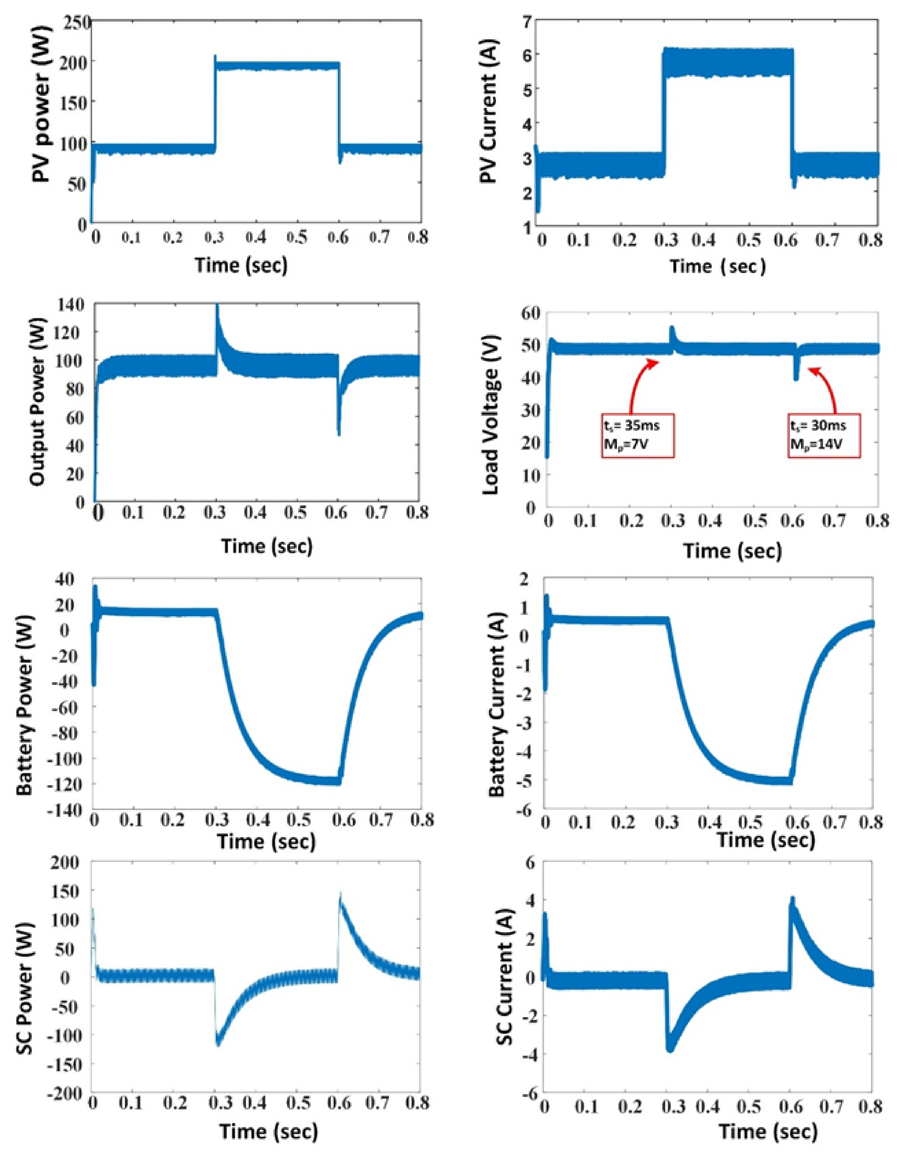
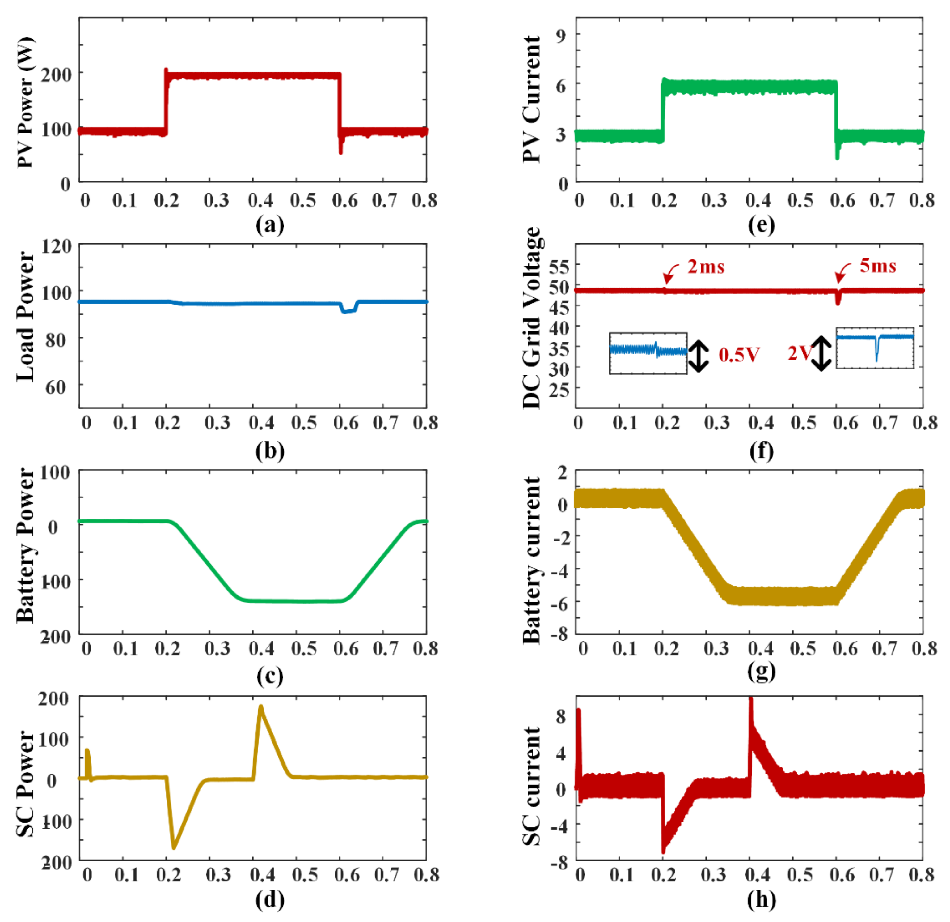
5.5. Step Change in PV Generation for Predictive PI Control Scheme

A step change in PV current is examined in this case. The peak overshoot (MP) settling time (tss) of DC Microgrid voltage during a step change in PV generation was examined. The load demand is kept constant in this case, by keeping Rdc = 24 Ω. By changing the PV current control reference, a step change in PV generation is applied to the steady-state system.
The simulation results for a step increase and decrease in PV generation are represented in Figure 20. Due to the atmosphere variations, power produced by the PV panel increases to 192 W from 96 W at t = 0.2 s and back to 96 W at t = 0.6 s. As PV power is more than the load power requirements, grid voltage increases beyond 48 V. The SC absorbs the excess power of 96 W in short time until the battery can regulate the grid voltage to 48 V.
In these cases, the transient current component is handled by the SC, with the steady-state current component supplied by the battery system. As PV generation increases or decreases, the change in DC bus voltage (ΔVDC) is 0.5 V and 2 V, respectively. The corresponding %MP values are 1.04% and 4.1%, respectively. Step increase and decrease in PV generation have settling times (tss) of 2 ms and 5 ms, respectively.

5.6. Step Change in Load Demand

The power developed by the PV panel is 96 W in the maximum power region. To absorb this PV power, the load resistance of 24 Ω is connected to a 48 V DC Microgrid. For consuming entire power from the PV panel, the load requires a 2 A current at a steady state. At t = 0.2 s, load demand increases from 96 W to 192 W and returns to 96 W at t = 0.6 s, as shown in Figure 21, which is beyond the power range of the PV panel. This creates a power imbalance between PV generation and load demand.
Immediately when the HESS responds, SC supplies a transient component of power and the battery supplies a steady-state component of power demand. As load demand increases or decreases, the changes in DC bus voltage (ΔVDC) are 3 V and 2.5 V, respectively. The corresponding %MP values are 6.25% and 5.2%, respectively. Step increases and decreases in load demand, with settling times (tss) of 3 ms and 10 ms, respectively.

5.7. Comparative Performance Evaluation

The graphical results’ representation of three control schemes is presented in Figure 22. The predictive PI scheme provides lesser overshoot, undershoot, and faster regulation with less settling time. Figure 22a,b shows the DC grid voltage variation with a step change in PV generation and load demand. Figure 22c,d shows the battery and SC current response with predictive PI over PI control strategies. In Figure 22d, we can see that the SC current is faster and higher compared to PI control methods. Hence, SC utilization is faster and higher compared to PI methods. Numerical comparisons of three control strategies are tabulated in Table 2. From the results, the performance of the predictive PI control method is better in terms of DC grid voltage regulation and SC utilization.

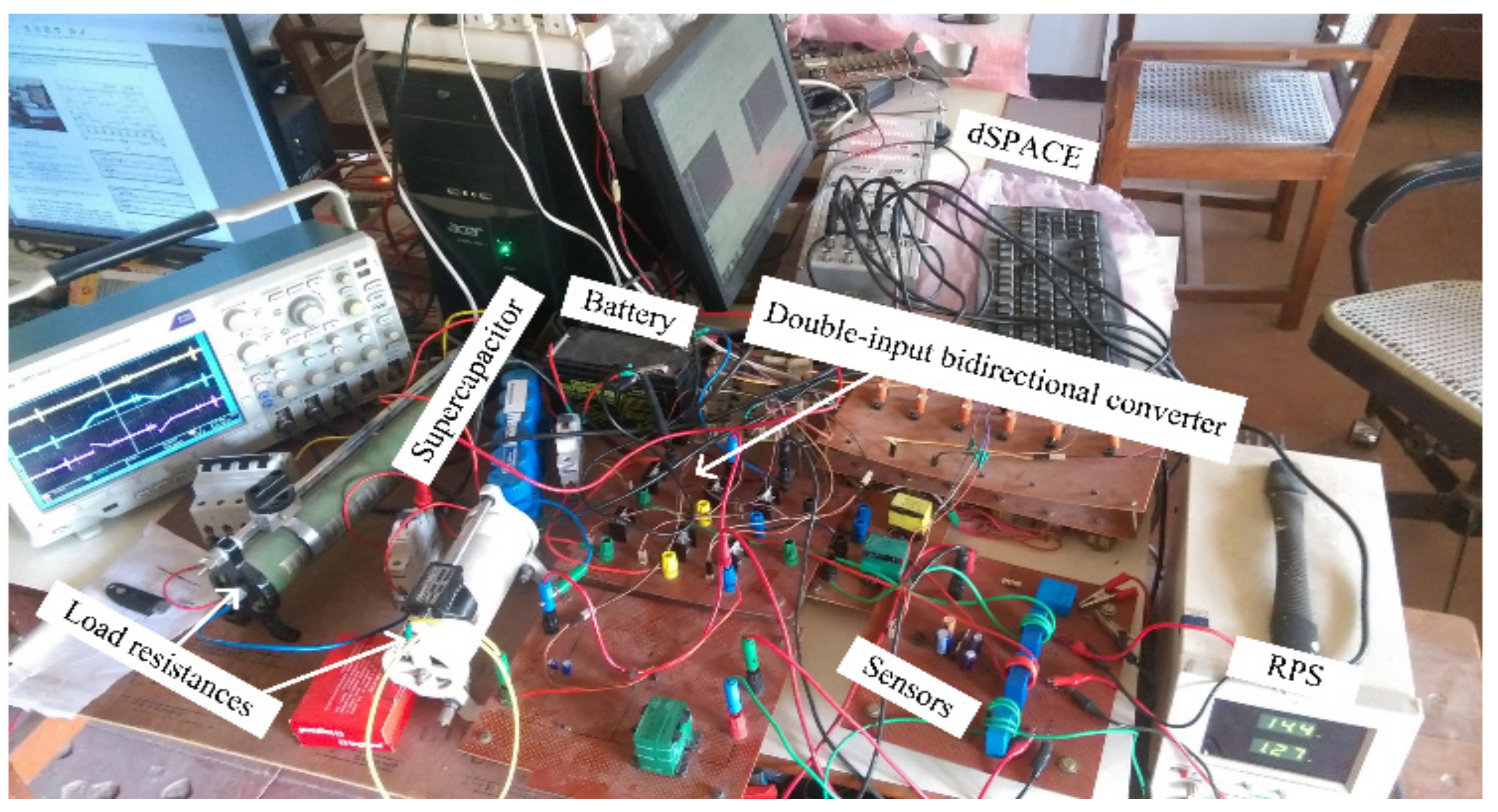
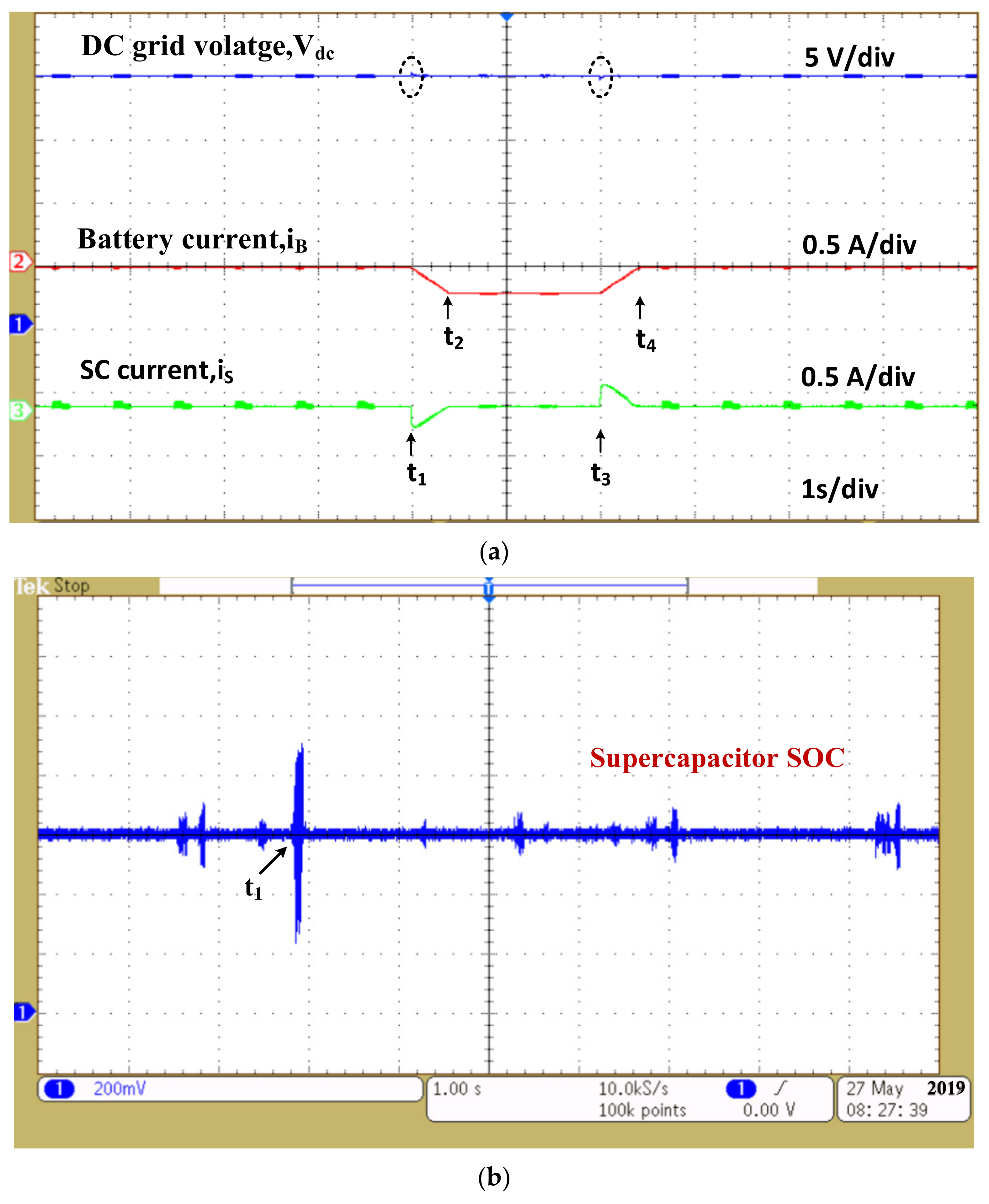
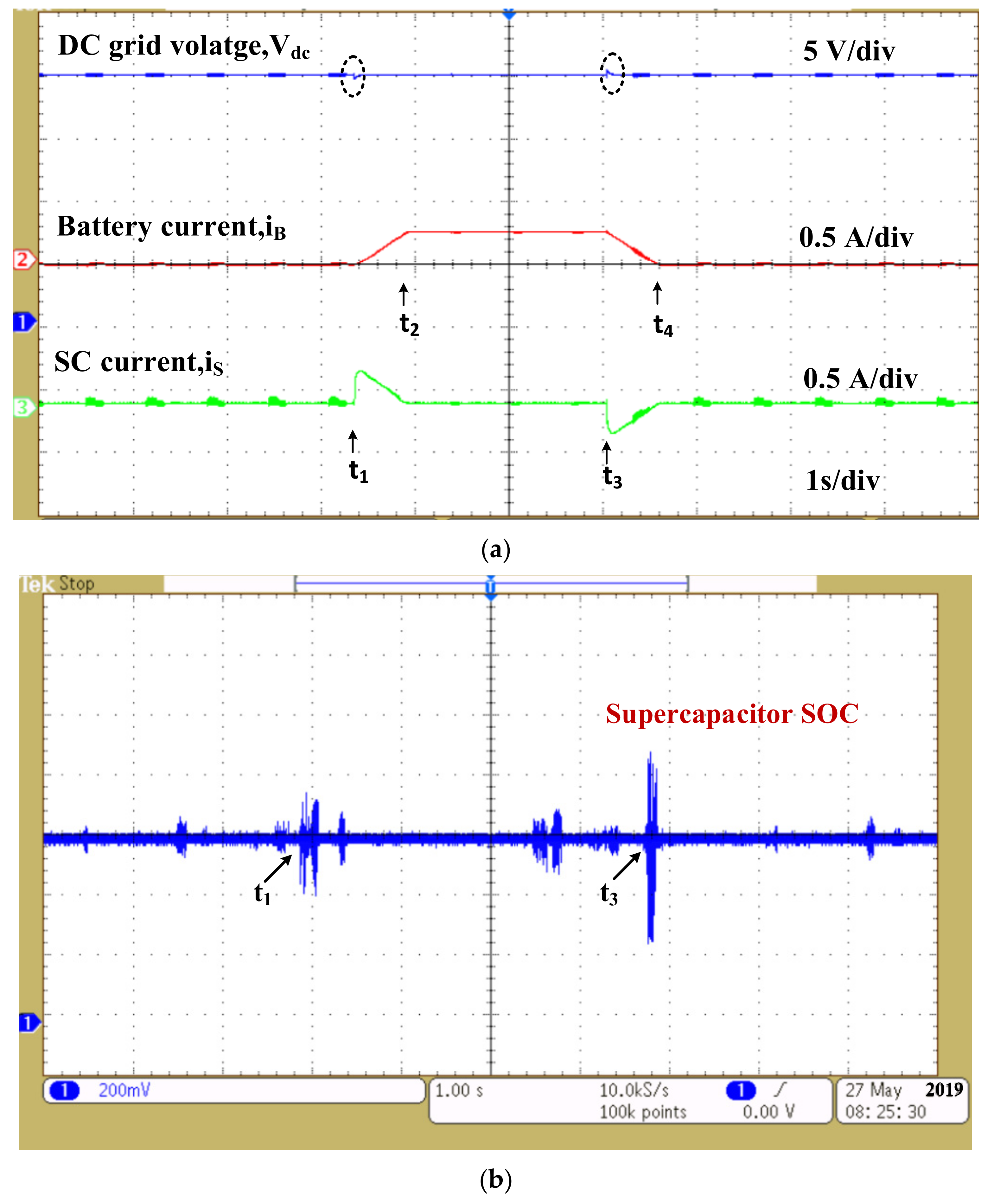
6. Experimental Results

As shown in Figure 23, a low-power hardware prototype model is developed to validate the efficiency of the proposed unified controller for a two-input bidirectional converter. The digital controller utilized is the dSPACE DS1104. A boost converter controls the current of a regulated power supply (RPS), which simulates the PV source. A HESS is powered by a single 12 V, 7 Ah Exide Chloride Safe power lead–acid battery and a single 16 V, 58 F Maxwell BMOD0058 supercapacitor. The bidirectional double-input converter is made up of six IRF540N MOSFET switches.
The performance of the DC Microgrid, which is powered by an emulated PV source and supported by a HESS, is validated in all three situations specified in Section 3: (1) HESS charging mode, (2) HESS discharging mode, and (3) HESS charging mode.
Table 3 shows the DC Microgrid specifications. The DC Microgrid is set up with a nominal voltage of 20 V.

6.1. HESS Charging Mode

Here, the performance of the designed controller in the scenario of a surge in DC Microgrid voltage, either due to increased PV generation or due to a decrease in load, is analyzed. Waveforms are given in Figure 24a,b. In this case, the surge in microgrid voltage is realized by increasing load resistance. Initially, the load resistance is R = 25 Ω up until instant t1. At t1, the load resistance is increased to 35 Ω and as a result of a decrease in load demand, the excess energy in the dc grid causes a surge in grid voltage. Immediately, the HESS responds in such a manner that the transient component of the current is the charging supercapacitor and the battery charging current is allowed to increase slowly until a steady-state value at instant t2.
The load resistance is brought back to the original condition of R = 25 Ω at instant t3. The battery and supercapacitor then return to their floating state as it was before t1. At instants t1 and t3, DC Microgrid voltage is retained at 20 V almost instantly, as indicated by small spikes in Figure 24a. The battery and supercapacitor SoC are shown in Figure 24b. At instant t1, SoCSC is shown to be increasing, indicating charging of the supercapacitor. After the transient current has died out, the supercapacitor remains idle, as indicated by constant SoC. Battery SoC is almost constant, with its energy not depleted quickly compared to the supercapacitor.

6.2. HESS Discharging Mode

In this case, the performance of the controller is pitted against the decrease in DC Microgrid voltage, either due to a decrease in PV generation or due to an increase in load. Waveforms are shown in Figure 25a,b. Here, a dip in DC Microgrid voltage is realized by a decrease in PV generation. A decrease in PV generation is implemented by decreasing the input current (IPV) of the boost converter connected to RPS while maintaining the input voltage (VPV) at 12 V.
At instant t1, IPV is decreased from 1.3 A to 1.1 A. This causes DC Microgrid voltage to dip since there exists a power mismatch between source and load. The deficient power is then fed by the HESS by discharging the battery and supercapacitor. Transient current is met by the supercapacitor and steady-state current is supplied by battery, as is evident from current waveforms in Figure 25a. The combined action of battery and supercapacitor maintain DC Microgrid voltage at the nominal value of 20 V. A small spike in voltage waveform is negligible due to the fast dynamics of the HESS. Battery charging current is allowed to increase slowly until a steady-state value at instant t2.
At instant t3, PV generation is reverted back to normal by setting IPV = 1.3 A. Battery current now slowly reduces to zero whereas the supercapacitor instantly responds to bring DC Microgrid voltage back to nominal value almost instantly. The battery and supercapacitor SoC waveform are also shown in Figure 25b to validate the above-explained operation. When PV generation is decreased at instant t1, SoC of SC is found to decrease as long as the supercapacitor supplies current indicating discharge operation of the supercapacitor. The supercapacitor is then idle, as indicated by the constant SoC waveform. Similarly, at instant t3, SoC is increased to indicate charging of the supercapacitor after which it stays idle.

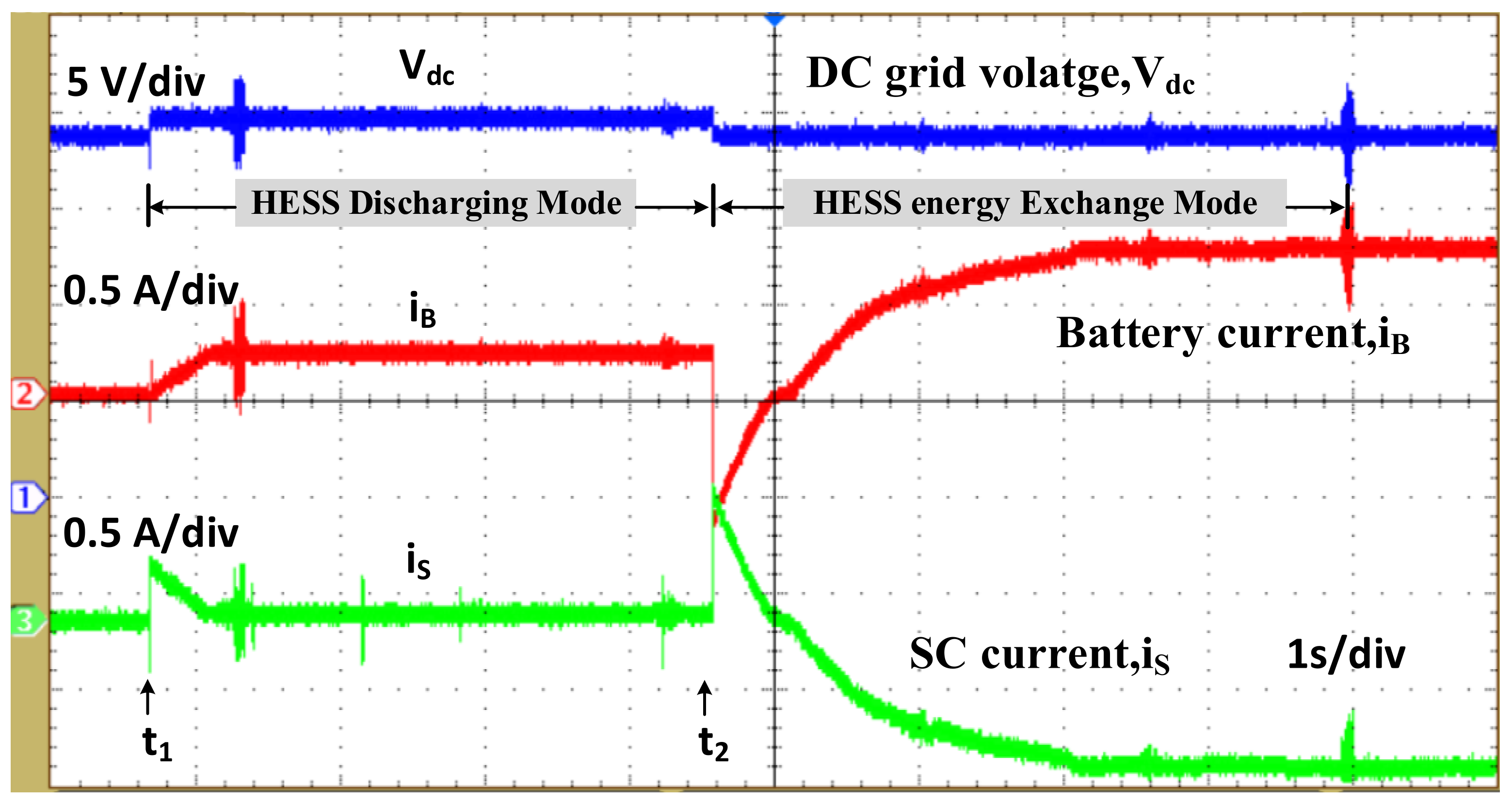
6.3. HESS Energy Exchange Mode

Power flow from the battery to the supercapacitor is depicted in this manner. Figure 26 depicts the waveforms. The HESS is unplugged from the DC Microgrid just before time instant t1. Due to reduced PV generation, the grid voltage is now 18 V. At instant t1, the HESS is active to produce grid voltage at the nominal value of 20 V. Battery and supercapacitor waveforms are as explained in HESS discharging mode. Current waveforms in Figure 26 prove the same result.

7. Conclusions

The controller for the two-input bidirectional converter was designed and modeled for the HESS controller. The developed controller’s performance was assessed in a range of scenarios for voltage regulation in a DC Microgrid. The controller could really balance out the DC Microgrid against unsettling influences from the source PV age, as well as burden varieties. It could take advantage of the supercapacitor’s inherent rapid dynamics to absorb incoming microgrid transients. This unique controller played a substantial role in both the charging and discharging process in the HESS. The operation mode of the HESS converter was also demonstrated for maintaining the supercapacitor’s SoC within the optimal range. A performance evaluation of the predictive PI and proposed PI over the conventional PI control scheme with a step change in PV generation and load demand for peak overshoot and settling time to restore grid voltage was performed. The results showed that the performance of the predictive PI control method is better in terms of DC grid voltage regulation and SC utilization.

Author Contributions

Conceptualization, S.P. and S.R.S.; methodology, S.P., S.B. and S.R.S.; simulation software, S.P.; validation, S.P. and S.B.; verification, S.B.; writing—review and editing, S.P., S.B. and S.R.S. All authors have read and agreed to the published version of the manuscript.

Funding

Woosong University’s Academic Research Funding—2022.

Institutional Review Board Statement

Not applicable.

Informed Consent Statement

Not applicable.

Data Availability Statement

Not applicable.

Conflicts of Interest

The authors declare no conflict of interest.

List of Symbols

dBBattery duty cycle
dSCSC duty cycle
fswSwitching frequency
iBBattery current
iB,refBattery reference current
iSCSC current
iSC,refSC reference current
VDCDC Microgrid voltage
VDC,refDC grid reference voltage
VBBattery voltage
VscSupercapacitor voltage
LBBattery inductance
LscSupercapacitor inductance
SoCiSupercapacitor’s initial state of charge
QscRated charge for Supercapacitor
itotTotal current from ESS
IHIGHHigh-frequency component of current
ILOWLow-frequency component of current
PstdSteady-state power component
PtranTransient power component
Pdc(t)DC grid power
Pren(t)RES power
Pb(t)Battery power
Psc(t)SC power
Kp,vProportional constant of the outer voltage loop
Ki,vIntegral constant of the outer voltage loop
verrVoltage error
PB_unUncompensated power from the battery system
iB,errBattery error current
iLPeak-to-peak inductor current
Gisc dSCControl-to-SC current transfer function
GVDCiSCSC current-to-output voltage transfer function
Gpi_iSPI controller transfer function of inner SC current loop
Gpi_vPI controller transfer function of the outer voltage control loop
GiBdBControl-to-battery current transfer function
Gpi_iBPI controller transfer function of battery current loop
Idc(k)Total load current
Vdc(k)Present sampling DC Microgrid voltage
Vsc(k)Present sampling SC voltage
Isc(k)Present sampling SC current
VB(k)Present sampling battery voltage
iB(k)Present sampling battery current
iB(k+1)Prediction of battery current
Isc(k+1)Prediction of SC current
iCCharging current
d v d c d t Rate of change of DC grid voltage
TsSampling period
d i b d t Rate of change of battery current
d i S C d t Rate of change of SC current
db(i)Iteratively calculated battery duty cycle
dSc(i)Iteratively calculated SC duty cycle
JObjective function of MPC

References

  1. Xiao, J.; Wang, P.; Setyawan, L. Implementation of Multiple-Slack-Terminal DC Microgrids for Smooth Transitions Between Grid-Tied and Islanded States. IEEE Trans. Smart Grid 2016, 7, 273–281. [Google Scholar] [CrossRef]
  2. Zadeh, M.K.; Gavagsaz-Ghoachani, R.; Pierfederici, S.; Nahid-Mobarakeh, B.; Molinas, M. Stability Analysis and Dynamic Performance Evaluation of a Power Electronics-Based DC Distribution System With Active Stabilizer. IEEE J. Emerg. Sel. Top. Power Electron. 2016, 4, 93–102. [Google Scholar] [CrossRef]
  3. Graditi, G.; Ippolito, M.G.; Telaretti, E.; Zizzo, G. An Innovative Conversion Device to the Grid Interface of Combined RES-Based Generators and Electric Storage Systems. IEEE Trans. Ind. Electron. 2015, 62, 2540–2550. [Google Scholar] [CrossRef]
  4. Choi, M.E.; Kim, S.W.; Seo, S.W. Energy Management Optimization in a Battery/Supercapacitor Hybrid Energy Storage System. IEEE Trans. Smart Grid 2012, 3, 463–472. [Google Scholar] [CrossRef]
  5. Feng, X.; Gooi, H.B.; Chen, S.X. Hybrid Energy Storage with Multimode Fuzzy Power Allocator for PV Systems. IEEE Trans. Sustain. Energy 2014, 5, 389–397. [Google Scholar] [CrossRef]
  6. Gao, L.; Dougal, R.A.; Liu, S. Power enhancement of an actively controlled battery/ultracapacitor hybrid. IEEE Trans. Power Electron. 2005, 20, 236–243. [Google Scholar] [CrossRef]
  7. Gee, M.; Robinson, F.V.P.; Dunn, R.W. Analysis of Battery Lifetime Extension in a Small-Scale Wind-Energy System Using Supercapacitors. IEEE Trans. Energy Convers. 2013, 28, 24–33. [Google Scholar] [CrossRef]
  8. Zheng, J.P.; Jow, T.R.; Ding, M.S. Hybrid power sources for pulsed current applications. IEEE Trans. Aerosp. Electron. Syst. 2001, 37, 288–292. [Google Scholar] [CrossRef]
  9. Lee, N.; Nee, C.H.; Yap, S.S.; Tham, K.K.; You, A.H.; Yap, S.L.; Mohd Arof, A.K.B. Capacity Sizing of Embedded Control Battery–Supercapacitor Hybrid Energy Storage System. Energies 2022, 15, 3783. [Google Scholar] [CrossRef]
  10. Zdiri, M.A.; Guesmi, T.; Alshammari, B.M.; Alqunun, K.; Almalaq, A.; Salem, F.B.; Hadj Abdallah, H.; Toumi, A. Design and Analysis of Sliding-Mode Artificial Neural Network Control Strategy for Hybrid PV-Battery-Supercapacitor System. Energies 2022, 15, 4099. [Google Scholar] [CrossRef]
  11. Mounica, V.; Obulesu, Y.P. Hybrid Power Management Strategy with Fuel Cell, Battery, and Supercapacitor for Fuel Economy in Hybrid Electric Vehicle Application. Energies 2022, 15, 4185. [Google Scholar] [CrossRef]
  12. Lencwe, M.J.; Chowdhury, S.P.D.; Olwal, T.O. An Effective Control for Lead-Acid Performance Enhancement in a Hybrid Battery-Supercapacitor System Used in Transport Vehicles. Sustainability 2021, 13, 13971. [Google Scholar] [CrossRef]
  13. Inthamoussou, F.A.; Pegueroles-Queralt, J.; Bianchi, F.D. Control of a Supercapacitor Energy Storage System for Microgrid Applications. IEEE Trans. Energy Convers. 2013, 28, 690–697. [Google Scholar] [CrossRef]
  14. Laldin, O.; Moshirvaziri, M.; Trescases, O. Predictive Algorithm for Optimizing Power Flow in Hybrid Ultracapacitor/Battery Storage Systems for Light Electric Vehicles. IEEE Trans. Power Electron. 2013, 28, 3882–3895. [Google Scholar] [CrossRef]
  15. Wang, B.; Xian, L.; Manandhar, U.; Ye, J.; Ukil, A.; Gooi, H.B. A stand-alone hybrid pv/fuel cell power systems using single-inductor dual-input single-output boost converter with model predictive control. In Proceedings of the 2017 Asian Conference on Energy, Power and Transportation Eletrification (ACEPT), Singapore, 24–26 October 2017; pp. 1–5. [Google Scholar]
  16. Zhao, C.; Round, S.D.; Kolar, J.W. An Isolated Three-Port Bidirectional DC-DC Converter With Decoupled Power Flow Management. IEEE Trans. Power Electron. 2008, 23, 2443–2453. [Google Scholar] [CrossRef]
  17. Zeng, J.; Qiao, W.; Qu, L.; Jiao, Y. An Isolated Multiport DC–DC Converter for Simultaneous Power Management of Multiple Different Renewable Energy Sources. IEEE J. Emerg. Sel. Top. Power Electron. 2014, 2, 70–78. [Google Scholar] [CrossRef]
  18. Wang, Y.; Han, F.; Yang, L.; Xu, R.; Liu, R. A Three-Port Bidirectional Multi-Element Resonant Converter With Decoupled Power Flow Management for Hybrid Energy Storage Systems. IEEE Access 2018, 6, 61331–61341. [Google Scholar] [CrossRef]
  19. Yang, P.; Tse, C.K.; Xu, J.; Zhou, G. Synthesis and Analysis of Double-Input Single-Output DC/DC Converter. IEEE Trans. Ind. Electron. 2015, 62, 6284–6295. [Google Scholar] [CrossRef]
  20. Khaligh, A.; Cao, J.; Lee, Y.J. A Multiple-Input DC–DC Converter Topology. IEEE Trans. Power Electron. 2009, 24, 862–868. [Google Scholar] [CrossRef]
  21. Wang, B.; Xian, L.; Manandhar, U.; Ye, J.; Zhang, X.; Gooi, H.B.; Ukil, A. Hybrid energy storage system using bidirectional single-inductor multipleport converter with model predictive control in DC microgrids. Electr. Power Syst. Res. 2019, 173, 38–47. [Google Scholar] [CrossRef]
  22. Faraji, R.; Farzanehfard, H. Soft-switching Nonisolated High step-up three-port DC-DC converter for Hybrid energy systems. IEEE Trans. Power Electron. 2018, 33, 10101–10111. [Google Scholar] [CrossRef]
  23. Mothilal Bhagavathy, S.; Pillai, G. PV Microgrid Design for Rural Electrification. Designs 2018, 2, 33. [Google Scholar] [CrossRef] [Green Version]
  24. Sato, Y.; Uno, M.; Nagata, H. Nonisolated Multiport Converters Based on Integration of PWM Converter and Phase-Shift-Switched Capacitor Converter. IEEE Trans. Power Electron. 2020, 35, 455–470. [Google Scholar] [CrossRef]
  25. Yi, Z.; Dong, W.; Etemadi, A.H. A Unified Control and Power Management Scheme for PV-Battery-Based Hybrid Microgrids for Both Grid-Connected and Islanded Modes. IEEE Trans. Smart Grid 2017, 9, 5975–5985. [Google Scholar] [CrossRef]
  26. Behjati, H.; Davoudi, A. Power Budgeting Between Diversified Energy Sources and Loads Using a Multiple-Input Multiple-Output DC-DC Converter. IEEE Trans. Ind. Appl. 2013, 49, 2761–2772. [Google Scholar] [CrossRef]
  27. Filsoof, K.; Lehn, P.W. A Bidirectional Multiple-Input Multiple-Output Modular Multilevel DC-DC Converter and its Control Design. IEEE Trans. Power Electron. 2016, 31, 2767–2779. [Google Scholar] [CrossRef]
  28. Wai, R.J.; Lin, C.Y.; Chen, B.H. High-Efficiency DC-DC Converter with Two Input Power Sources. IEEE Trans. Power Electron. 2012, 27, 1862–1875. [Google Scholar] [CrossRef]
  29. Nejabatkhah, F.; Danyali, S.; Hosseini, S.H.; Sabahi, M.; Niapour, S.M. Modeling and Control of a New Three-Input DC–DC Boost Converter for Hybrid PV/FC/Battery Power System. IEEE Trans. Power Electron. 2012, 27, 2309–2324. [Google Scholar] [CrossRef]
  30. Wai, R.J.; Chen, B.H. High-Efficiency Dual-Input Interleaved DC-DC Converter for Reversible Power Sources. IEEE Trans. Power Electron. 2014, 29, 2903–2921. [Google Scholar] [CrossRef]
  31. Chen, C.W.; Liao, C.Y.; Chen, K.H.; Chen, Y.M. Modeling and Controller Design of a Semiisolated Multiinput Converter for a Hybrid PV/Wind Power Charger System. IEEE Trans. Power Electron. 2015, 30, 4843–4853. [Google Scholar] [CrossRef]
  32. Danyali, S.; Hosseini, S.H.; Gharehpetian, G.B. New Extendable Single-Stage Multi-input DC–DC/AC Boost Converter. IEEE Trans. Power Electron. 2014, 29, 775–788. [Google Scholar] [CrossRef]
  33. Guo, F.; Fu, L.; Zhang, X.; Yao, C.; Li, H.; Wang, J. A Family of Quasi-Switched-Capacitor Circuit-Based Dual-Input DC/DC Converters for Photovoltaic Systems Integrated With Battery Energy Storage. IEEE Trans. Power Electron. 2016, 31, 8237–8246. [Google Scholar] [CrossRef]
  34. Gummi, K.; Ferdowsi, M. Double-Input DC–DC Power Electronic Converters for Electric-Drive Vehicles—Topology Exploration and Synthesis Using a Single-Pole Triple-Throw Switch. IEEE Trans. Ind. Electron. 2010, 57, 617–623. [Google Scholar] [CrossRef]
  35. Karpana, S.; Batzelis, E.; Maiti, S.; Chakraborty, C. PV-Supercapacitor Cascaded Topology for Primary Frequency Responses and Dynamic Inertia Emulation. Energies 2021, 14, 8347. [Google Scholar] [CrossRef]
  36. Ahrabi, R.R.; Ardi, H.; Elmi, M.; Ajami, A. A Novel Step-Up Multiinput DC–DC Converter for Hybrid Electric Vehicles Application. IEEE Trans. Power Electron. 2017, 32, 3549–3561. [Google Scholar] [CrossRef]
  37. Akar, F.; Tavlasoglu, Y.; Ugur, E.; Vural, B.; Aksoy, I. A Bidirectional Nonisolated Multi-Input DC–DC Converter for Hybrid Energy Storage Systems in Electric Vehicles. IEEE Trans. Veh. Technol. 2016, 65, 7944–7955. [Google Scholar] [CrossRef]
  38. Nahavandi, A.; Hagh, M.T.; Sharifian, M.B.B.; Danyali, S. A Nonisolated Multiinput Multioutput DC–DC Boost Converter for Electric Vehicle Applications. IEEE Trans. Power Electron. 2015, 30, 1818–1835. [Google Scholar] [CrossRef]
  39. Hintz, A.; Prasanna, U.R.; Rajashekara, K. Novel Modular Multiple-Input Bidirectional DC–DC Power Converter (MIPC) for HEV/FCV Application. IEEE Trans. Ind. Electron. 2015, 62, 3163–3172. [Google Scholar] [CrossRef]
  40. Punna, S.; Mailugundla, R.; Salkuti, S.R. Design, Analysis and Implementation of Bidirectional DC–DC Converters for HESS in DC Microgrid Applications. Smart Cities 2022, 5, 433–454. [Google Scholar] [CrossRef]
  41. Kachhwaha, A.; Rashed, G.I.; Garg, A.R.; Mahela, O.P.; Khan, B.; Shafik, M.B.; Hussien, M.G. Design and Performance Analysis of Hybrid Battery and Ultracapacitor Energy Storage System for Electrical Vehicle Active Power Manage-ment. Sustainability 2022, 14, 776. [Google Scholar] [CrossRef]
  42. Hsieh, M.-F.; Chen, P.-H.; Pai, F.-S.; Weng, R.-Y. Development of Supercapacitor-Aided Hybrid Energy Storage System to Enhance Battery Life Cycle of Electric Vehicles. Sustainability 2021, 13, 7682. [Google Scholar] [CrossRef]
  43. Park, S.; Salkuti, S.R. Optimal Energy Management of Railroad Electrical Systems with Renewable Energy and Energy Storage Systems. Sustainability 2019, 11, 6293. [Google Scholar] [CrossRef] [Green Version]
  44. Kollimalla, S.K.; Mishra, M.K. A novel adaptive p & o mppt algorithm considering sudden changes in the irradiance. IEEE Trans. Energy Convers. 2014, 29, 602–610. [Google Scholar]
Figure 1. Various configurations of a HESS consisting of a battery connected to a DC Microgrid and an SC. (a) Two segregated bidirectional converter modules. (b) Bidirectional converter with single double-input.
Information 13 00350 g001
Figure 2. HESS-enhanced DC Microgrid with PV source.
Information 13 00350 g002
Figure 3. HESS with double-input bidirectional converter topology.
Information 13 00350 g003
Figure 4. Consistent state waveforms for HESS Discharging Sequence.
Information 13 00350 g004
Figure 5. Steady state waveforms for HESS charging mode of operation.
Information 13 00350 g005
Figure 6. HESS mode of energy exchange. (a) Current flows across an active circuit. (b) Waveforms in a steady state.
Information 13 00350 g006
Figure 7. A flow chart depicts transitions between distinct modes.
Information 13 00350 g007
Figure 8. Overall management mechanism for current bifurcation between SC and battery units for conventional PI.
Information 13 00350 g008
Figure 9. Overall management mechanism for current bifurcation between SC and battery units for proposed PI.
Information 13 00350 g009
Figure 10. Logic for controlling a supercapacitor and a battery. (a) The supercapacitor control scheme. (b) Battery control system scheme.
Information 13 00350 g010
Figure 11. Bode plot of SC’s inner current controller of logic for control, both with and without controller.
Information 13 00350 g011
Figure 12. Bode plot of SC’s outer voltage controller of logic for control, both with and without controller.
Information 13 00350 g012
Figure 13. Bode plot of battery control logic’s current controller.
Information 13 00350 g013
Figure 14. Block diagram of predictive PI control scheme for a HESS.
Information 13 00350 g014
Figure 15. Supercapacitor SoC charge controller. (a) Charging and discharging logic; logic for the charging and discharging process. (b) Flowchart of the control logic.
Information 13 00350 g015
Figure 16. Simulation results for step change in PV generation for conventional PI controller.
Information 13 00350 g016
Figure 17. Simulation results for step change in PV generation for proposed PI control scheme.
Information 13 00350 g017
Figure 18. Simulation results for step change in load demand for conventional PI control scheme.
Information 13 00350 g018
Figure 19. Simulation results for step change in load demand for proposed PI control scheme.
Information 13 00350 g019
Figure 20. Simulation results for step change in PV generation for predictive PI control scheme.
Information 13 00350 g020
Figure 21. Simulation results for step change in load demand for predictive PI control scheme.
Information 13 00350 g021
Figure 22. Comparative analysis of conventional PI, proposed PI, and predictive PI control schemes. (a,b) DC grid voltage for step change in PV and load, (c) battery current, (d) SC current.
Information 13 00350 g022
Figure 23. Low-power hardware developed a prototype model.
Information 13 00350 g023
Figure 24. Experimental results for HESS charging mode.
Information 13 00350 g024
Figure 25. Experimental results for HESS discharging mode.
Information 13 00350 g025
Figure 26. Experimental results for energy exchange mode.
Information 13 00350 g026
Table 1. Specification parameters for simulation study.
S. NoSpecification ParametersValue
1Voltage at MPPT(Vmppt)32 V
2Current of MPPT (Imppt)2 A
3Power at MPPT (Pmppt)96 W
3Supercapacitor voltage (VSC)32 V
4Supercapacitor inductance (LS)0.355 mH
5Battery voltage (VB)24 V
6Inductance in Battery (LB)0.3 mH
7Inductance in Boost converter (L)4.1 mH
8Resistance (R) in the Converter4.8 Ω
9Voltage in DC Microgrid (VDC)48 V
10Capacitance (C)300 µF
Table 2. Comparative performance of various control methods.
Conventional PIProposed PIPredictive PI
Settling
Time (tss)
%MPSettling
Time (tss)
%MPSettling
Time (tss)
%MP
Step increase in
PV generation
100 ms22.9%35 ms14.58%2 ms0.01%
Step decrease in
PV generation
120 ms27%30 ms14.5%5 ms4.1%
Step increase in
load demand
100 ms25%40 ms12.5%3 ms6.25%
Step decrease in
load demand
80 ms29.16%30 ms16.6%10 ms5.2%
Table 3. DC Microgrid implementation parameters.
S. NoParametersValue
1SC voltage (VSC)10 V
2SC inductance (LS)1.43 mH
3Battery voltage (VB)12 V
4Battery inductance (LB)4.8 mH
5Boost inductance (L)4.1 mH
6Resistance (R)25 Ω
7DC Microgrid voltage (VDC)20 V
8Capacitance (C)150 µF
Publisher’s Note: MDPI stays neutral with regard to jurisdictional claims in published maps and institutional affiliations.

