
Fault-Tolerant Multiport Active Bridge Converter for Resilient Energy Storage Integration in Zonal Shipboard DC System


Abstract
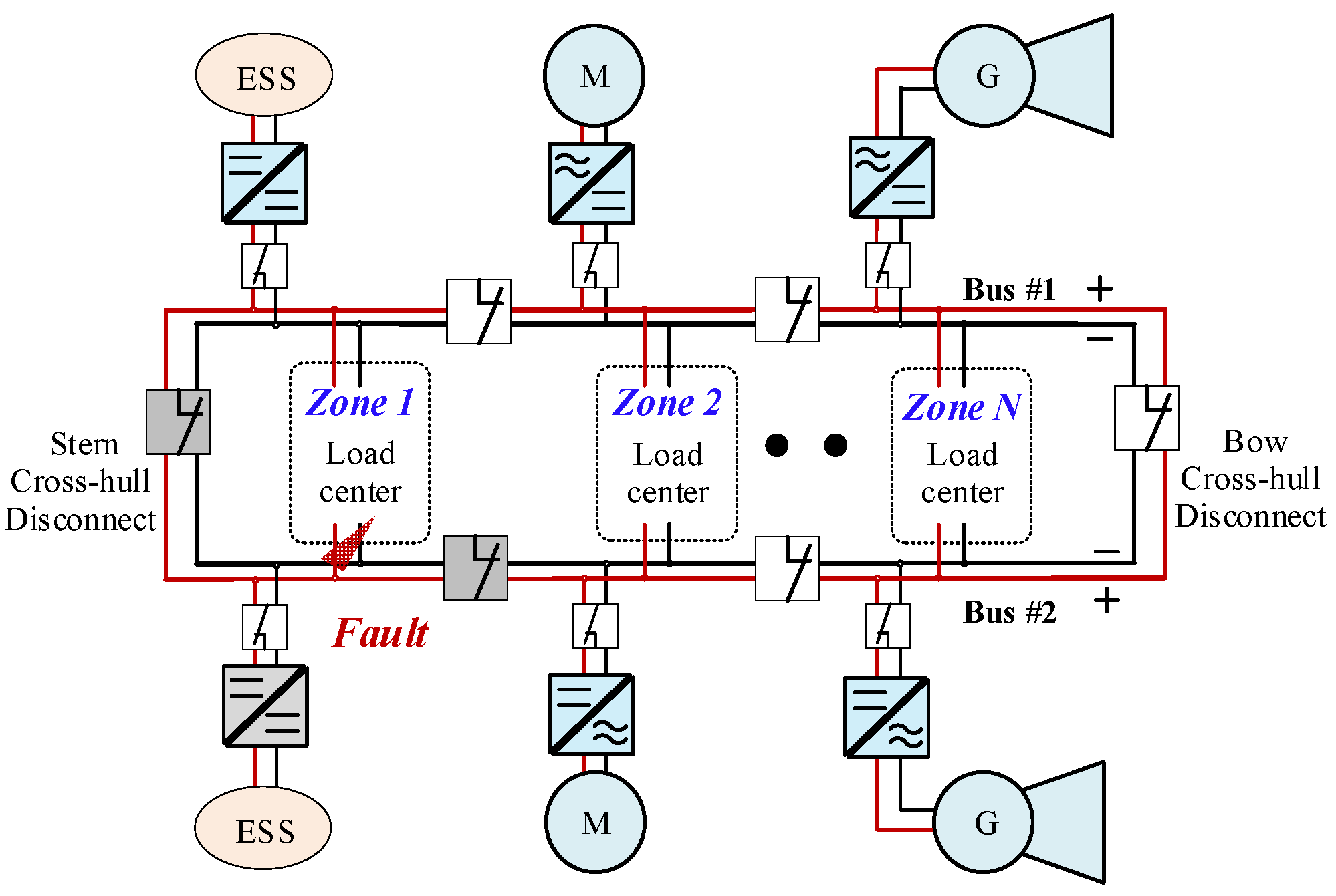
1. Introduction

| Integrated Multiport Design | Fault-Tolerant Operation | References |
|---|---|---|
 |  | [18,20,22] |
| | [8,21,27] |
| | Proposed work |
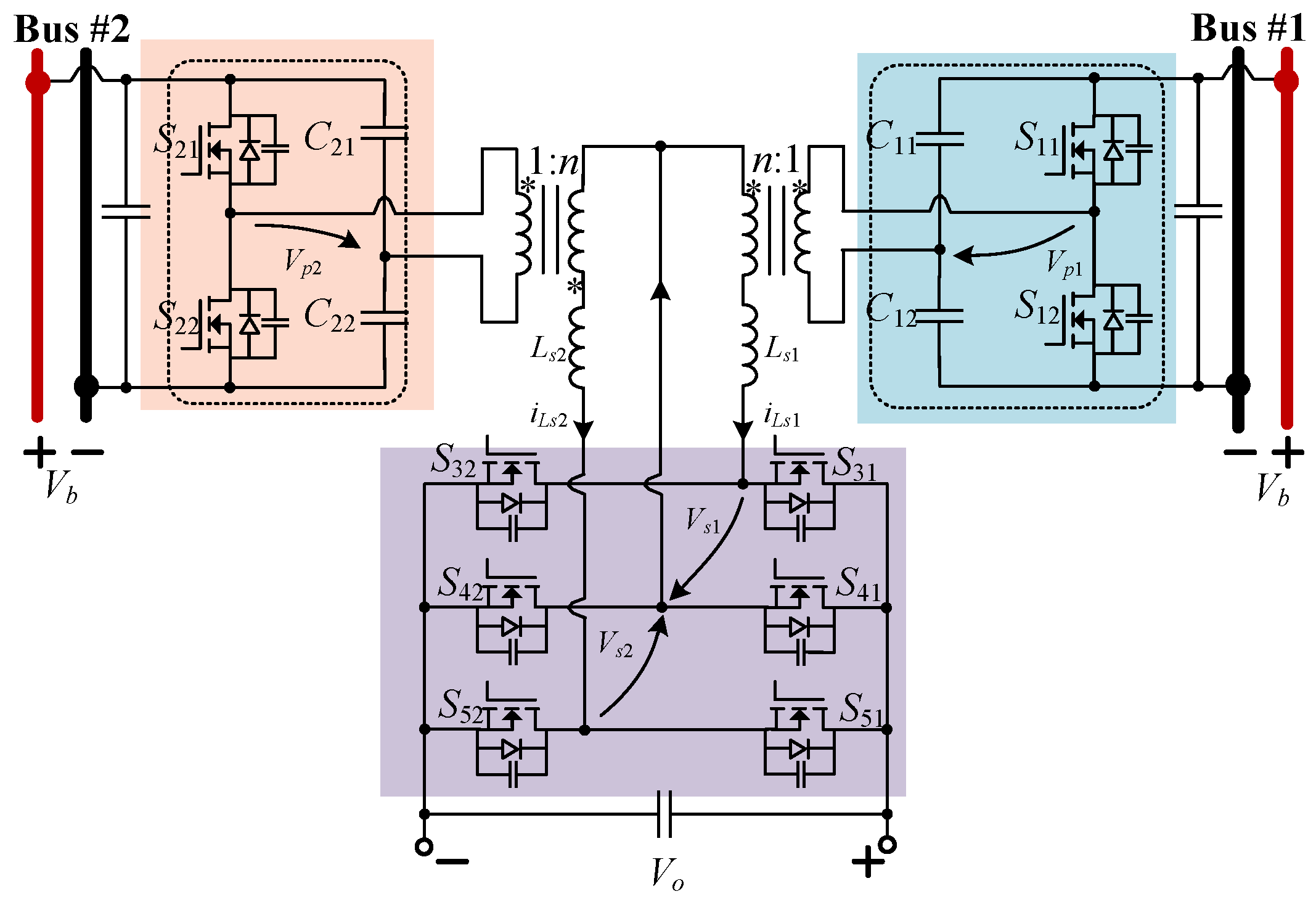
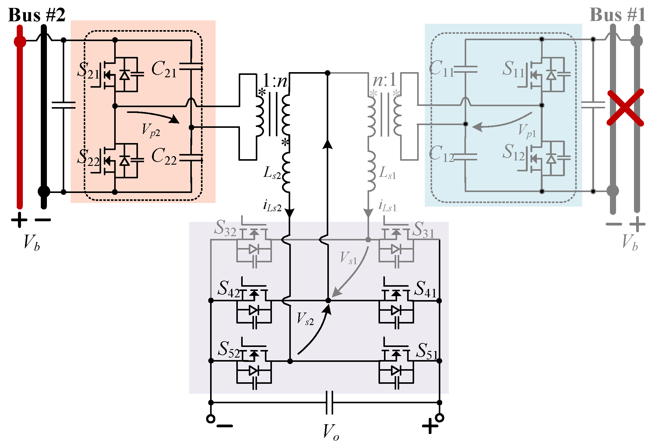
2. Operation Principles
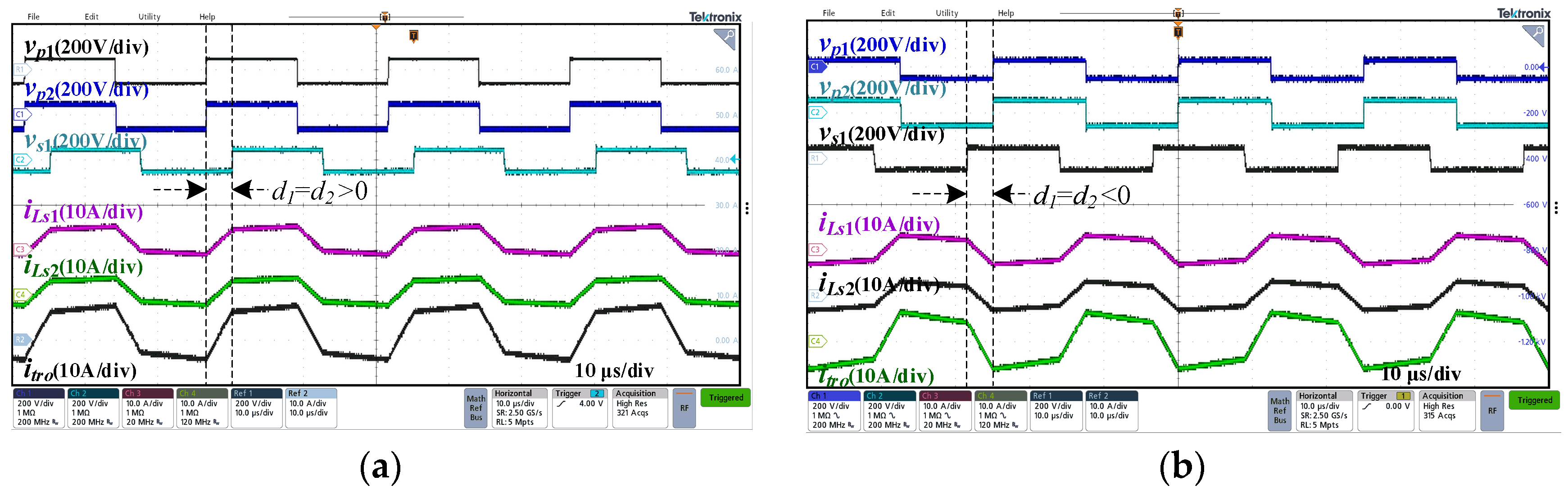
2.1. Normal Operation
2.1.1. Same Power Direction of DC Buses
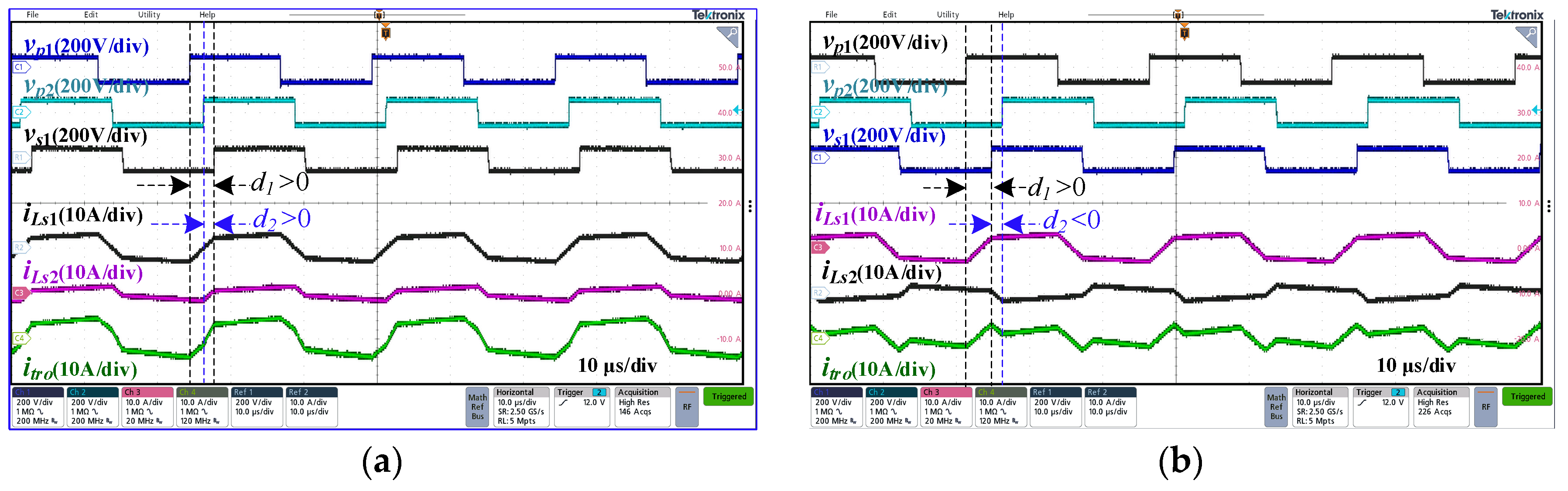
2.1.2. Mutual Power Support Between DC Buses
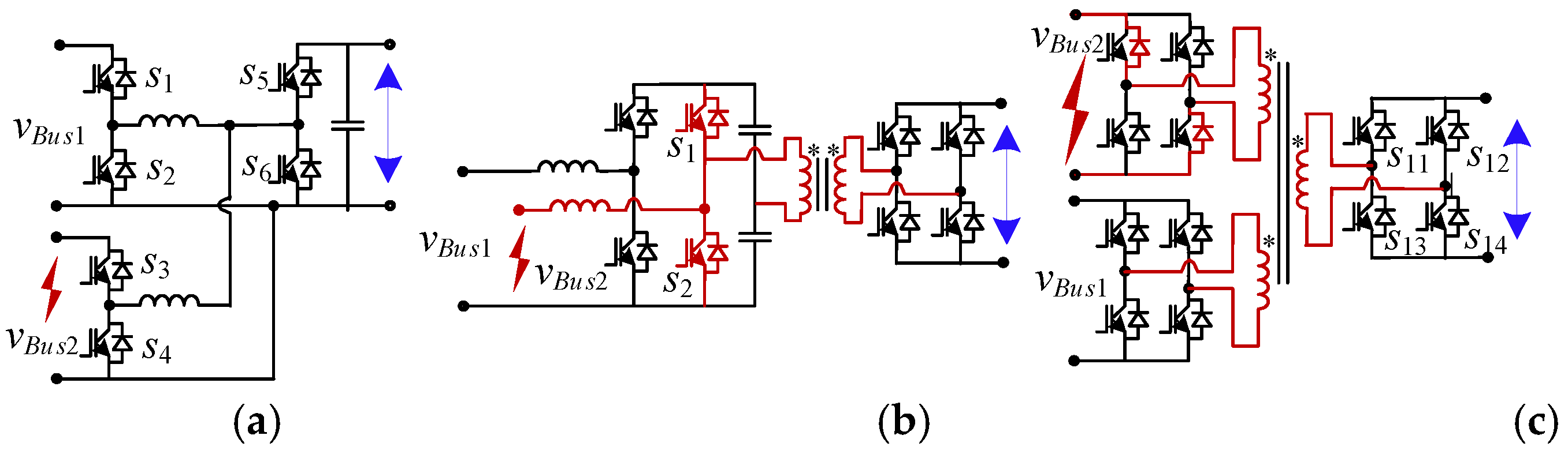
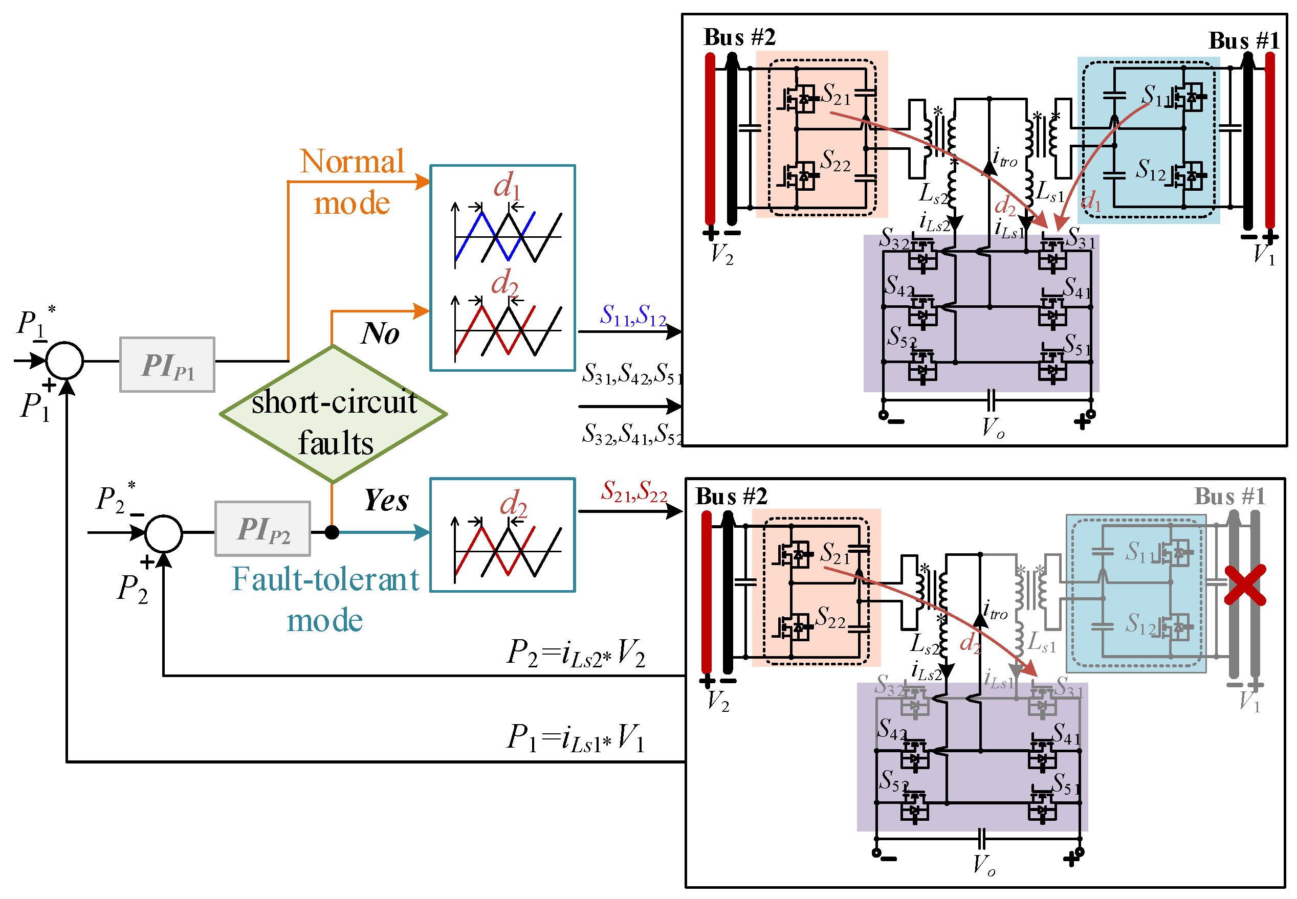
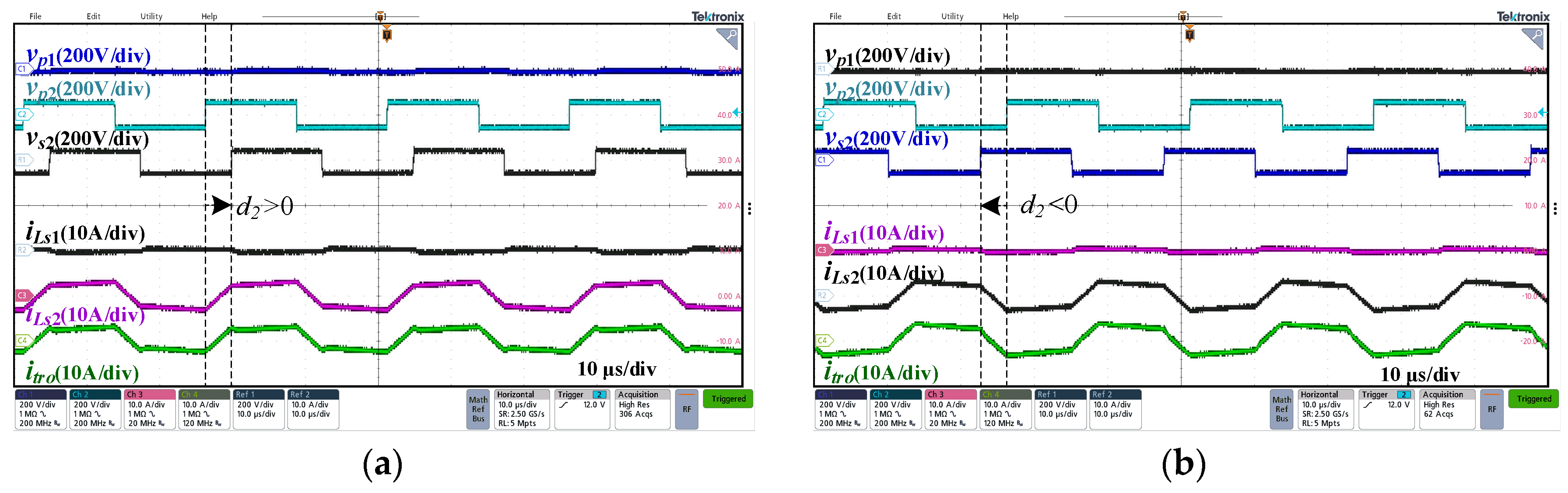
2.2. Fault-Tolerant Operation
3. Performance Analysis
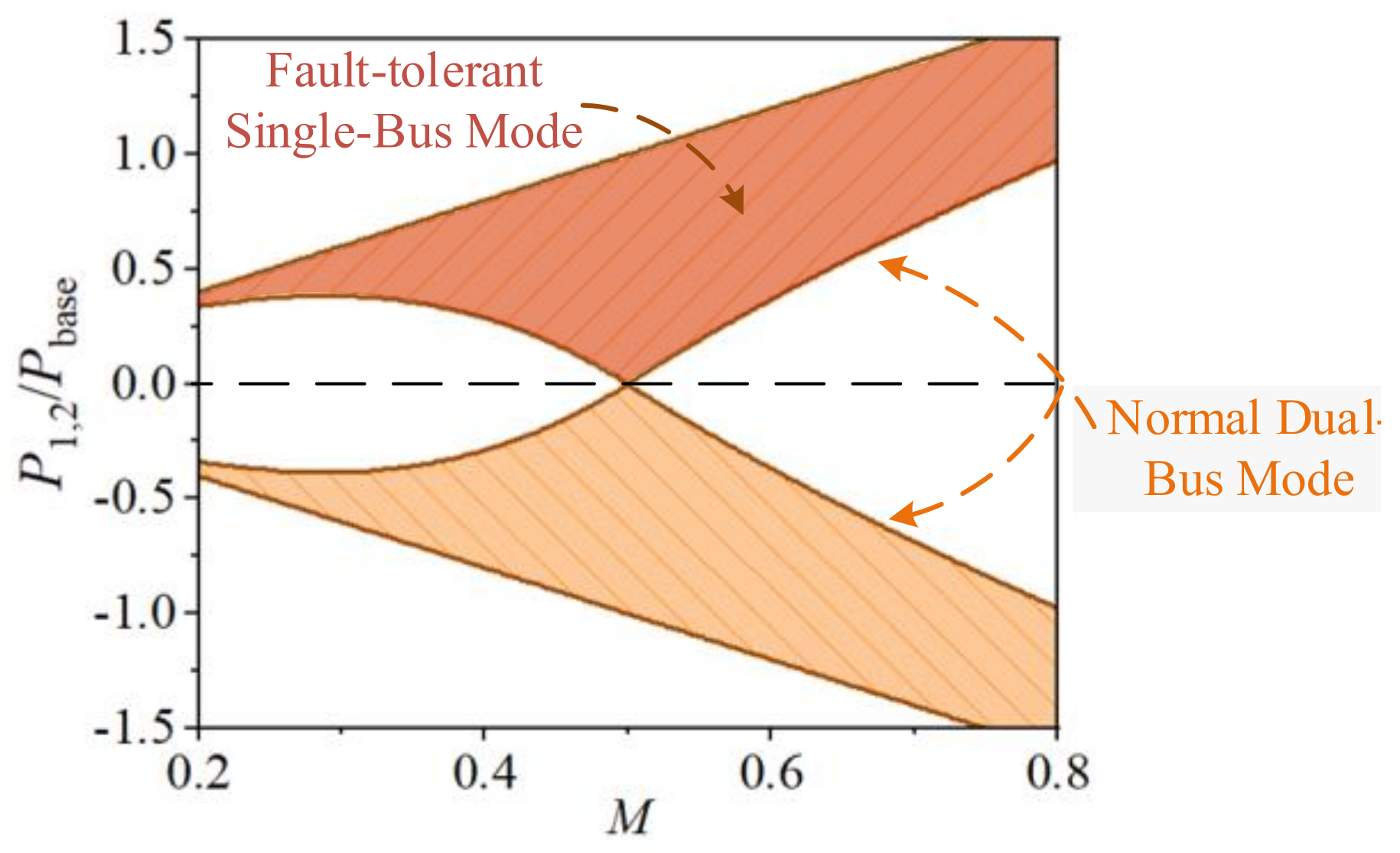
3.1. Power Transfer Capability
3.2. Soft Switching Performance
3.3. Control Design
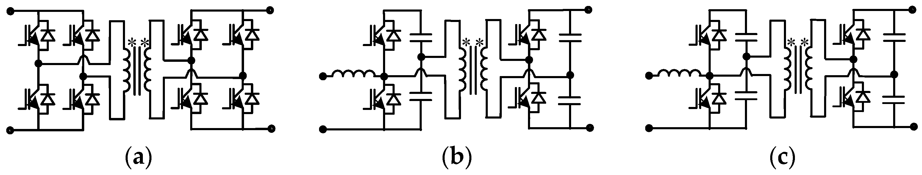
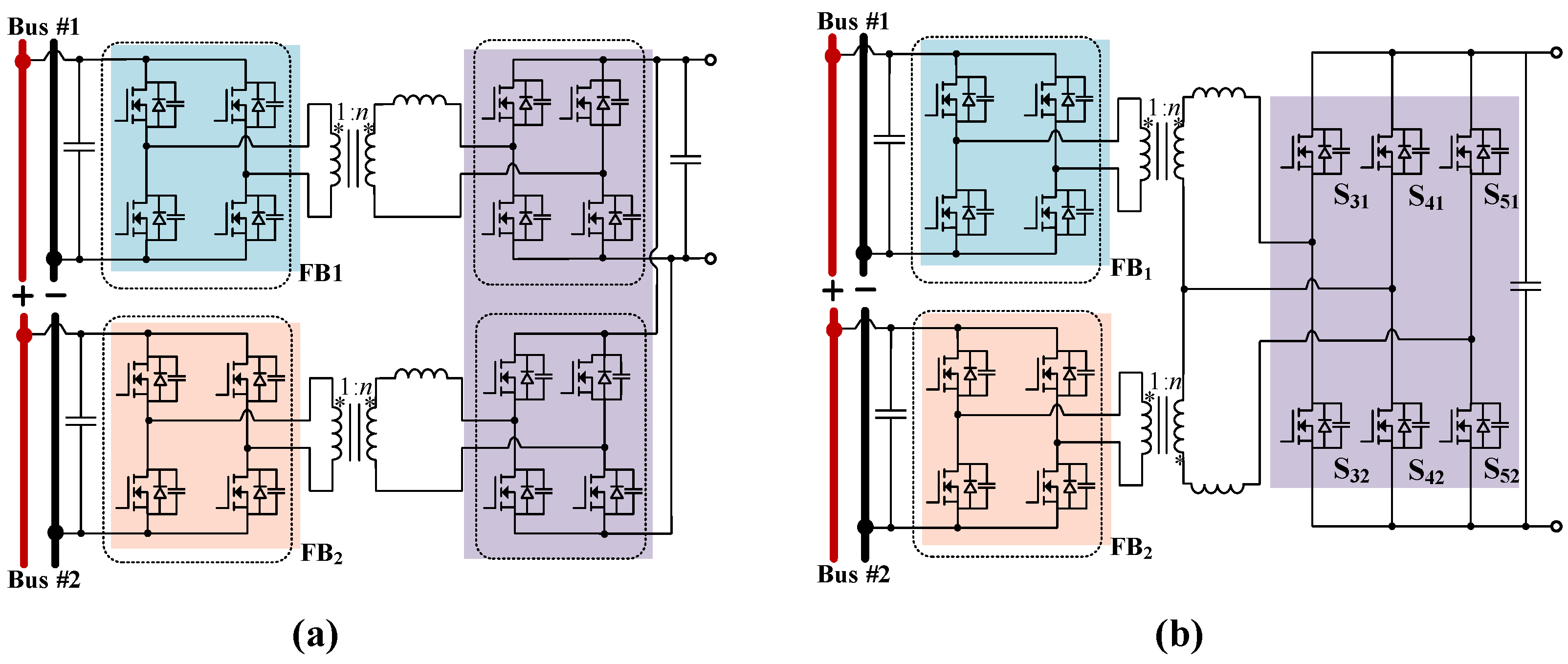
4. Circuit Comparison
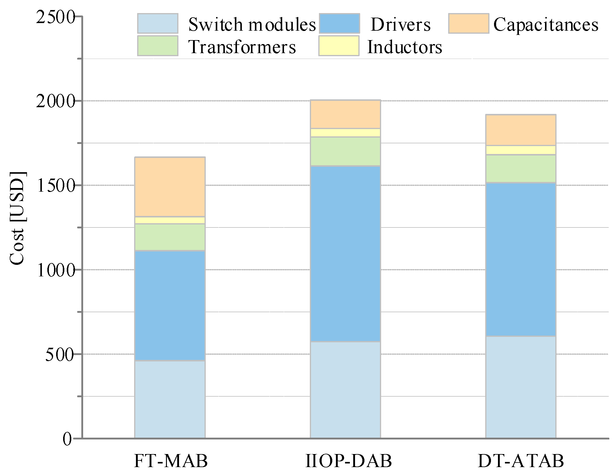
4.1. Cost Comparison
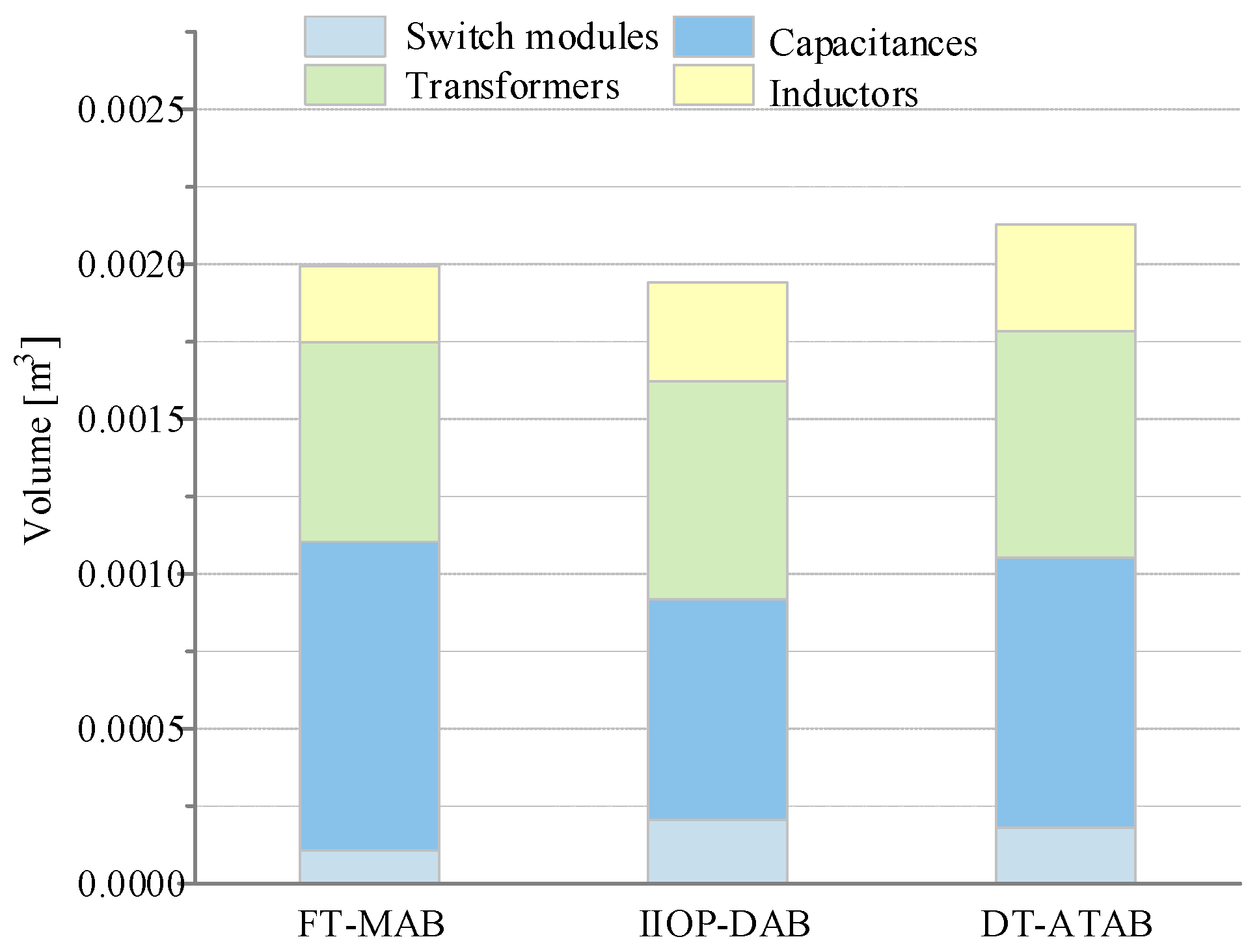
4.2. Volume Comparison
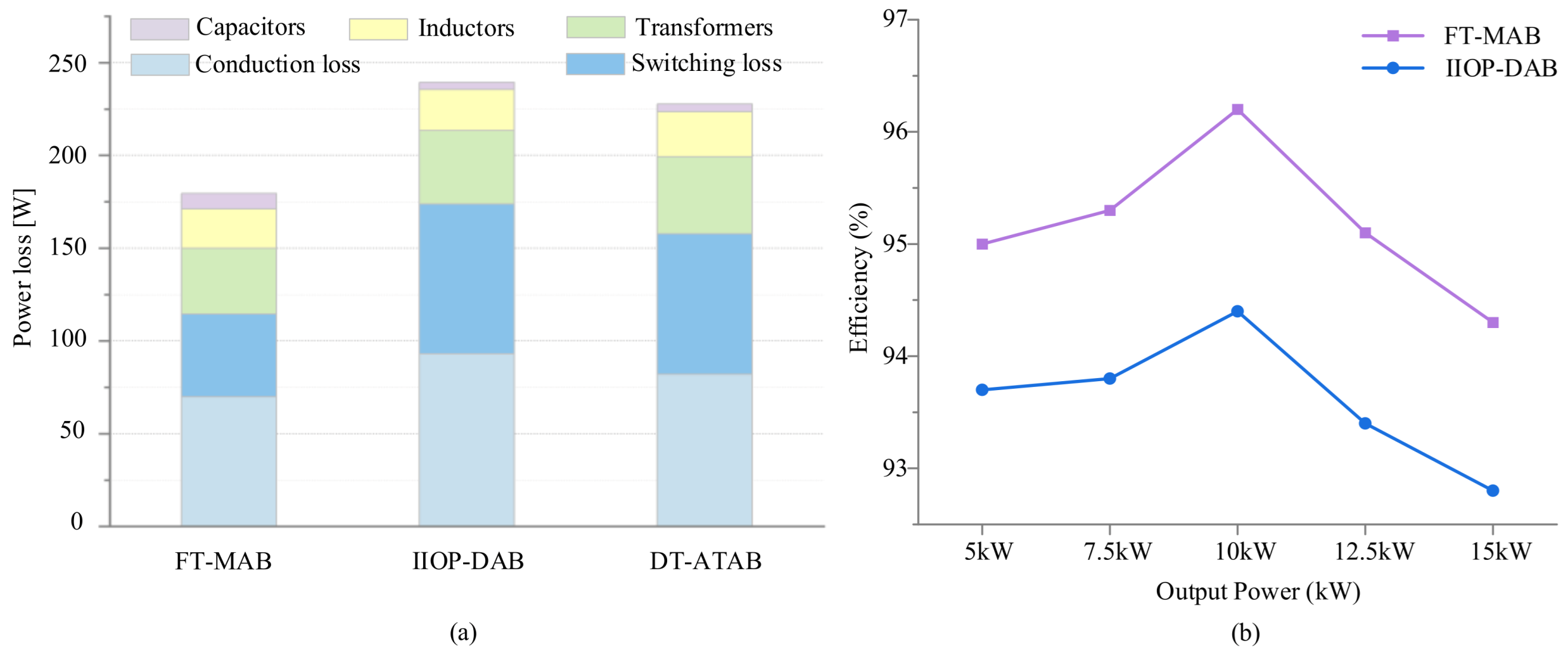
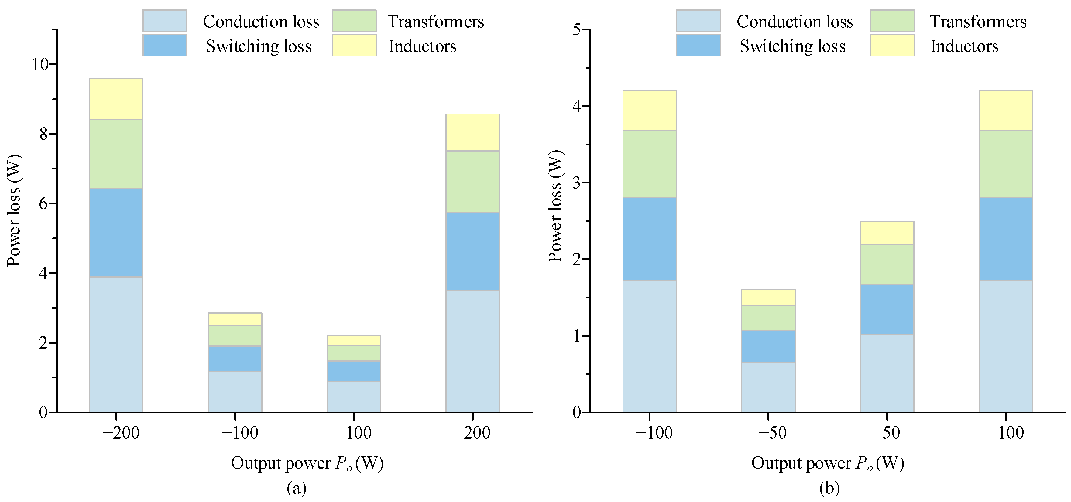
4.3. Loss Comparison
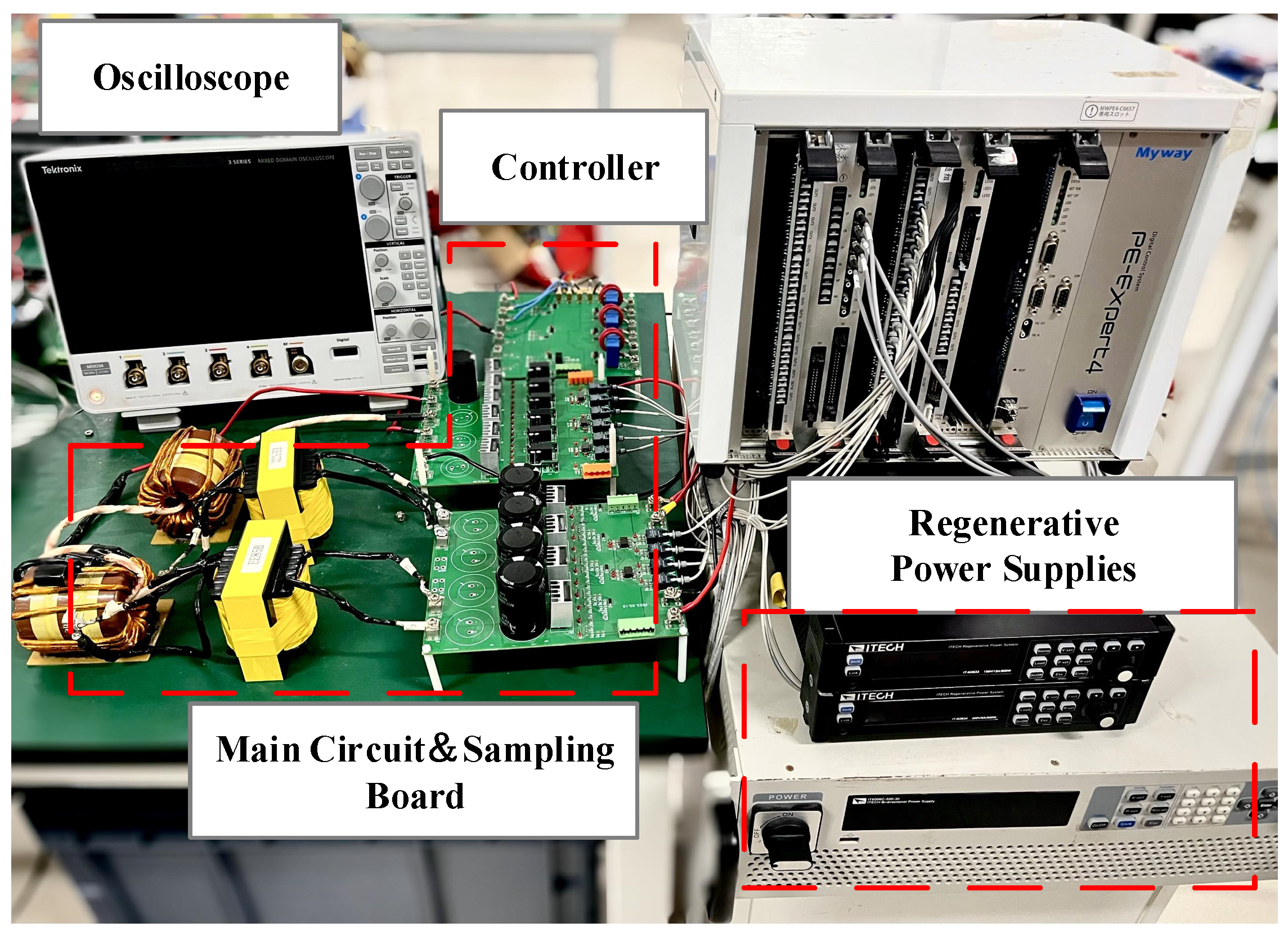
5. Experimental Verifications
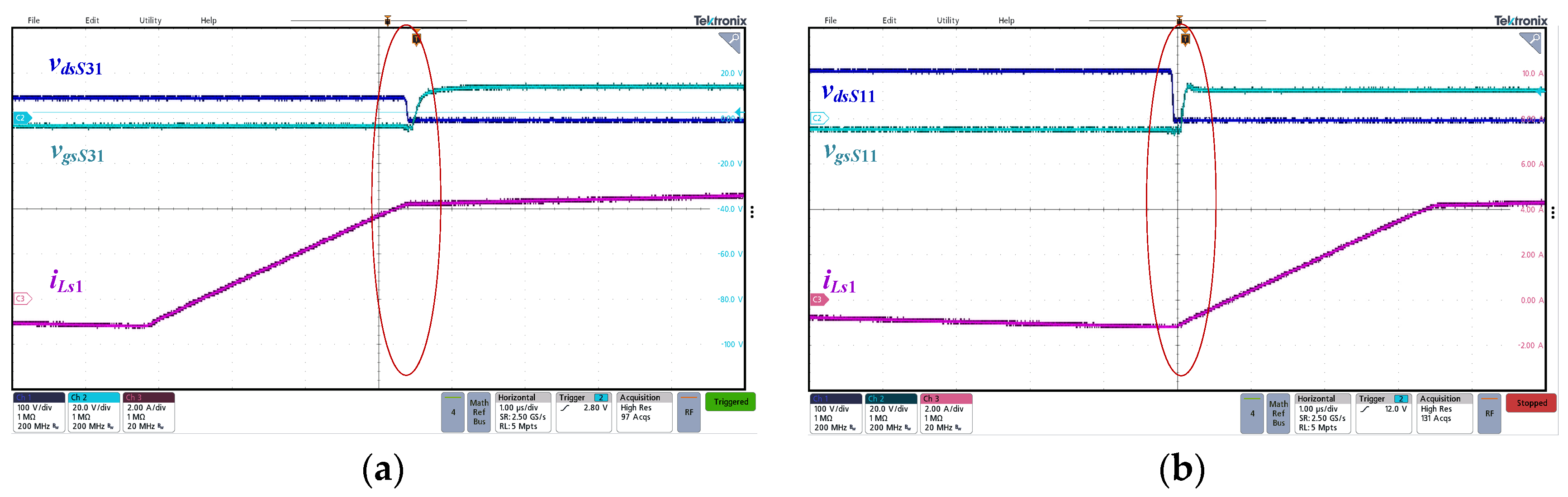
5.1. Steady-State Operation and ZVS Characteristics
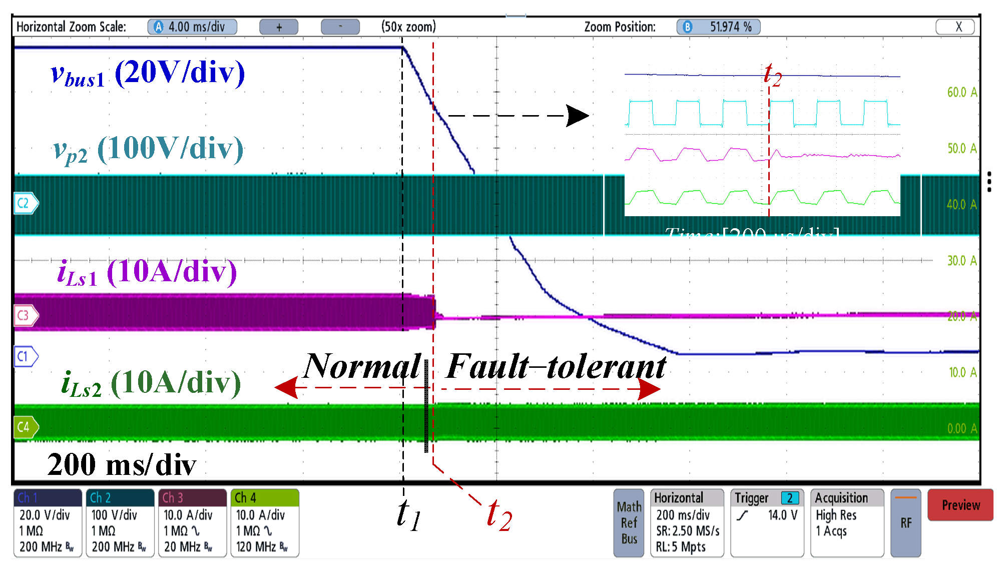
5.2. Fault-Tolerant Operation
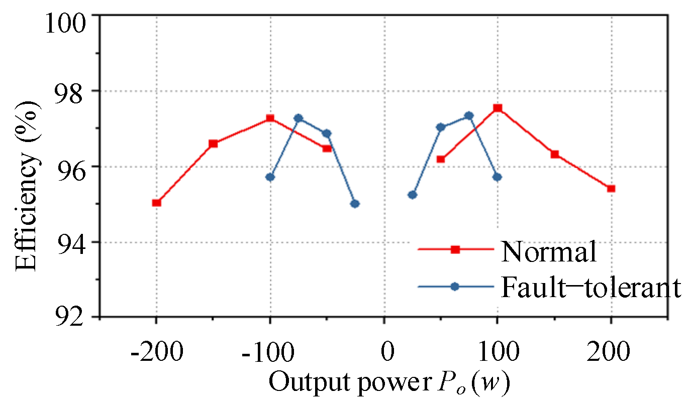
5.3. Efficiency
6. Conclusions
- ■
- The proposed FT-MAB converter enables bidirectional power regulation between the energy storage and the two DC buses, as well as mutual power support between the DC buses;
- ■
- In the event of a short-circuit fault, the FT-MAB converter can isolate the fault port and maintain uninterrupted power supply to the healthy bus;
- ■
- Compared to the traditional dual-converter zonal configuration, the proposed topology can maintain fault-tolerant operation and reduce the converter power loss as well as cost.
Author Contributions
Funding
Data Availability Statement
Conflicts of Interest
References
- IEEE Std 1709-2018 (Revision of IEEE Std 1709-2010); IEEE Recommended Practice for 1 kV to 35 kV Medium-Voltage DC Power Systems on Ships. IEEE: Piscataway, NJ, USA, 2018; pp. 1–54.
- Sulligoi, G.; Vicenzutti, A.; Menis, R. All-Electric Ship Design: From Electrical Propulsion to Integrated Electrical and Electronic Power Systems. IEEE Trans. Transp. Electrif. 2016, 2, 507–521. [Google Scholar]
- Wen, S.; Jin, X.; Zheng, Y.; Wang, M. Probabilistic Coordination of Optimal Power Management and Voyage Scheduling for All-Electric Ships. IEEE Trans. Transp. Electrif. 2024, 10, 3661–3669. [Google Scholar]
- Xu, L.; Guerrero, J.M.; Lashab, A.; Wei, B.; Bazmohammadi, N.; Vasquez, J.C.; Abusorrah, A. A Review of DC Shipboard Microgrids—Part I: Power Architectures, Energy Storage, and Power Converters. IEEE Trans. Power Electron. 2022, 37, 5155–5172. [Google Scholar]
- Zohrabi, N.; Shi, J.; Abdelwahed, S. An overview of design specifications and requirements for the MVDC shipboard power system. Int. J. Electr. Power Energy Syst. 2019, 104, 680–693. [Google Scholar]
- Jin, Z.; Sulligoi, G.; Cuzner, R.; Meng, L.; Vasquez, J.C.; Guerrero, J.M. Next-Generation Shipboard DC Power System: Introduction Smart Grid and dc Microgrid Technologies into Maritime Electrical Netowrks. IEEE Electrif. Mag. 2016, 4, 45–57. [Google Scholar]
- Latorre, A.; Soeiro, T.B.; Geertsma, R.; Coraddu, A.; Polinder, H. Shipboard DC Systems—A Critical Overview: Challenges in Primary Distribution, Power-Electronics-Based Protection, and Power Scalability. IEEE Open. J. Ind. Elec. 2023, 4, 259–286. [Google Scholar]
- Sulligoi, G.; Bosich, D.; Vicenzutti, A.; Khersonsky, Y. Design of Zonal Electrical Distribution Systems for Ships and Oil Platforms: Control Systems and Protections. IEEE Trans. Ind. Appl. 2020, 56, 5656–5669. [Google Scholar]
- Baran, M.E.; Mahajan, N. System reconfiguration on shipboard DC zonal electrical system. In Proceedings of the IEEE Electric Ship Technologies Symposium, Philadelphia, PA, USA, 27 July 2005; pp. 86–92. [Google Scholar]
- Maqsood, A.; Corzine, K.A. Integration of Z-Source Breakers Into Zonal DC Ship Power System Microgrids. IEEE J. Emerg. Sel. Top. Power Electron. 2017, 5, 269–277. [Google Scholar]
- Hou, N.; Li, Y.W. Overview and Comparison of Modulation and Control Strategies for a Nonresonant Single-Phase Dual-Active-Bridge DC–DC Converter. IEEE Trans. Power Electron. 2020, 35, 3148–3172. [Google Scholar]
- Shi, H.; Sun, K.; Wu, H.; Li, Y. A Unified State-Space Modeling Method for a Phase-Shift Controlled Bidirectional Dual-Active Half-Bridge Converter. IEEE Trans. Power Electron. 2020, 35, 3254–3265. [Google Scholar]
- Jung, J.-H.; Kim, H.-S.; Ryu, M.-H.; Baek, J.-W. Design Methodology of Bidirectional CLLC Resonant Converter for High-Frequency Isolation of DC Distribution Systems. IEEE Trans. Power Electron. 2013, 28, 1741–1755. [Google Scholar] [CrossRef]
- Kang, X.; Li, S.; Smedley, K.M. Decoupled PWM Plus Phase-Shift Control for a Dual-Half-Bridge Bidirectional DC–DC Converter. IEEE Trans. Power Electron. 2018, 33, 7203–7213. [Google Scholar]
- Jakka, V.N.S.R.; Shukla, A.; Demetriades, G.D. Dual-Transformer-Based Asymmetrical Triple-Port Active Bridge (DT-ATAB) Isolated DC–DC Converter. IEEE Trans. Ind. Electron. 2017, 64, 4549–4560. [Google Scholar] [CrossRef]
- Chen, Y.; Ma, J.; Zhu, M.; Liu, J. Dual-Mode Wide-Voltage-Range Operation of Hybrid Triple Active Bridge Converter for Bipolar DC Distribution Systems. IEEE Trans. Ind. Appl. 2024, 60, 8998–9014. [Google Scholar] [CrossRef]
- Wang, Z.; Luo, Q.; Wei, Y.; Mou, D.; Lu, X.; Sun, P. Topology Analysis and Review of Three-Port DC–DC Converters. IEEE Trans. Power Electron. 2020, 35, 11783–11800. [Google Scholar] [CrossRef]
- Zhang, H.; Dong, D.; Liu, W.; Ren, H.; Zheng, F. Systematic Synthesis of Multiple-Input and Multiple-Output DC–DC Converters for Nonisolated Applications. IEEE J. Emerg. Sel. Top. Power Electron. 2022, 10, 6470–6481. [Google Scholar] [CrossRef]
- Sato, Y.; Uno, M.; Nagata, H. Nonisolated Multiport Converters Based on Integration of PWM Converter and Phase-Shift-Switched Capacitor Converter. IEEE Trans. Power Electron. 2020, 35, 455–470. [Google Scholar] [CrossRef]
- Tao, H. Integration of Sustainable Energy Sources Through Power Electronic Converters in Small Distributed Electricity Generation Systems. Ph.D. Dissertation, Electrical Engineering, Technische Universiteit Eindhoven, Eindhoven, The Netherlands, 2008. [Google Scholar]
- Ma, J.; Zhu, M.; Li, Y.; Cai, X. Monopolar Fault Reconfiguration of Bipolar Half Bridge Converter for Reliable Load Supply in DC Distribution System. IEEE Trans. Power Electron. 2022, 37, 11305–11318. [Google Scholar] [CrossRef]
- Yang, W.; Ma, J.; Zhu, M.; Hu, C. Open-Circuit Fault Diagnosis and Tolerant Method of Multiport Triple Active-Bridge DC-DC Converter. IEEE Trans. Ind. Appl. 2023, 59, 5473–5487. [Google Scholar] [CrossRef]
- Zhang, H.; Yu, H.; Zhang, Q.; Wang, Y.; Chen, Z. Fault Current Suppression for the Fault Ride-Through of Triple-Active-Bridge Converters. IEEE Trans. Ind. Electron. 2024, 71, 10727–10738. [Google Scholar] [CrossRef]
- Xiao, Z.; Zeng, Y.; Tang, Y. Swift and Seamless Start-Up of DAB Converters in Constant and Variable Frequency Modes. IEEE Trans. Ind. Electron. 2024. [Google Scholar] [CrossRef]
- Zeng, Y.; Xiao, Z.; Liu, Q. Physics-Informed Deep Transfer Reinforcement Learning Method for the Input-Series Output-Parallel Dual Active Bridge-Based Auxiliary Power Modules in Electrical Aircraft. IEEE Trans. Transp. Electrif. 2024. [Google Scholar] [CrossRef]
- IEEE Std 1826-2020 (Revision of IEEE Std 1826-2012); IEEE Standard for Power Electronics Open System Interfaces in Zonal Electrical Distribution Systems Rated Above 100 kW. IEEE: Piscataway, NJ, USA, 2020; pp. 1–44. [CrossRef]
- Satpathi, K.; Ukil, A.; Pou, J. Short-circuit fault management in DC electric ship propulsion system: Protection requirements review of existing technologies and future research trends IEEE Trans. IEEE Trans. Transp. Electrif. 2018, 4, 272–291. [Google Scholar]
- Digikey Electronics. 2024. Available online: https://www.digikey.cn/zh (accessed on 15 October 2024).
- Magnetics-Inductor Design Tool. 2024. Available online: https://designtools.mag-inc.com/inductor/ (accessed on 28 October 2024).


| Switches | S11, S12 | S21, S22 | S31, S32 | S41, S42 | S51, S52 |
|---|---|---|---|---|---|
| ZVS Criterion d1 > 0 and d2 > 0 (in Figure 6a) | iLs1(t0) < 0 | iLs2(t1) < 0 | iLs1(t2) > 0 | itro(t2) > 0 | iLs2(t2) > 0 |
| ZVS Criterion d1 > 0 and d2 < 0 (in Figure 6b) | iLs1(t0) < 0 | iLs2(t2) < 0 | iLs1(t1) > 0 | itro(t1) > 0 | iLs2(t1) > 0 |
| Switches | S21, S22 | S41, S42 | S51, S52 |
|---|---|---|---|
| ZVS Criterion (in Figure 8) | iLs2(t1) < 0 | itro(t2) > 0 | iLs2(t2) > 0 |
| Parameter | Value |
|---|---|
| Bus voltage Vbus1, Vbus2 | 750 V, 750 V |
| Output power Po | 15 kW |
| Output voltage Vo | 400 V |
| Switching frequency fs | 40 kHz |
| Items | Proposed | IIOP-DAB | DT-ATAB | |
|---|---|---|---|---|
| Peak current through switches/A | Input-side | 27 | 17 | 17 |
| Output-side | 60 | 30 | 60 | |
| Switches | Input-side | FF33MR12W1M1HP_B11 | ||
| Output- side | FF33MR12W1M1HP_B11 | |||
| Output- shared switches (S41,S42) | FF6MR 12W2M1H_B11 | / | FF6MR12W2M1H_B11 | |
| Magnetic components | Transformer core | 0P49925UC | ||
| turns ratio n | 1 | 0.5 | 0.5 | |
| Inductor core | 0077774A7 | |||
| Capacitors | Bus-side | B32373B4107J080 | C44USGT6120M81K | |
| Load-side | B32371A3806J030 | C4DEIPQ6100A8TK | B25631B0127K800 | |
| Driver | 2ASC-12A2HP | |||
| Parameter | Value |
|---|---|
| Input voltage Vbus1, Vbus2 | 48 V |
| Output voltage Vo | 110 V |
| Rated output power Por | 200 W |
| Switching frequency fs | 40 kHz |
| Series inductance Ls | 65 μH |
| Transformer turns ratio | 1:1 |
Disclaimer/Publisher’s Note: The statements, opinions and data contained in all publications are solely those of the individual author(s) and contributor(s) and not of MDPI and/or the editor(s). MDPI and/or the editor(s) disclaim responsibility for any injury to people or property resulting from any ideas, methods, instructions or products referred to in the content. |
© 2025 by the authors. Licensee MDPI, Basel, Switzerland. This article is an open access article distributed under the terms and conditions of the Creative Commons Attribution (CC BY) license (https://creativecommons.org/licenses/by/4.0/).
Share and Cite
Ma, J.; Chen, Y.; Shen, X.; Qiu, Y. Fault-Tolerant Multiport Active Bridge Converter for Resilient Energy Storage Integration in Zonal Shipboard DC System. J. Mar. Sci. Eng. 2025, 13, 654. https://doi.org/10.3390/jmse13040654
Ma J, Chen Y, Shen X, Qiu Y. Fault-Tolerant Multiport Active Bridge Converter for Resilient Energy Storage Integration in Zonal Shipboard DC System. Journal of Marine Science and Engineering. 2025; 13(4):654. https://doi.org/10.3390/jmse13040654
Chicago/Turabian StyleMa, Jianjun, Yijia Chen, Xianger Shen, and Yixiong Qiu. 2025. "Fault-Tolerant Multiport Active Bridge Converter for Resilient Energy Storage Integration in Zonal Shipboard DC System" Journal of Marine Science and Engineering 13, no. 4: 654. https://doi.org/10.3390/jmse13040654
APA StyleMa, J., Chen, Y., Shen, X., & Qiu, Y. (2025). Fault-Tolerant Multiport Active Bridge Converter for Resilient Energy Storage Integration in Zonal Shipboard DC System. Journal of Marine Science and Engineering, 13(4), 654. https://doi.org/10.3390/jmse13040654