
Underwater Power Conversion and Junction Technology for Underwater Wireless Power Transfer Stations

 , ,
, ,
Abstract
1. Introduction
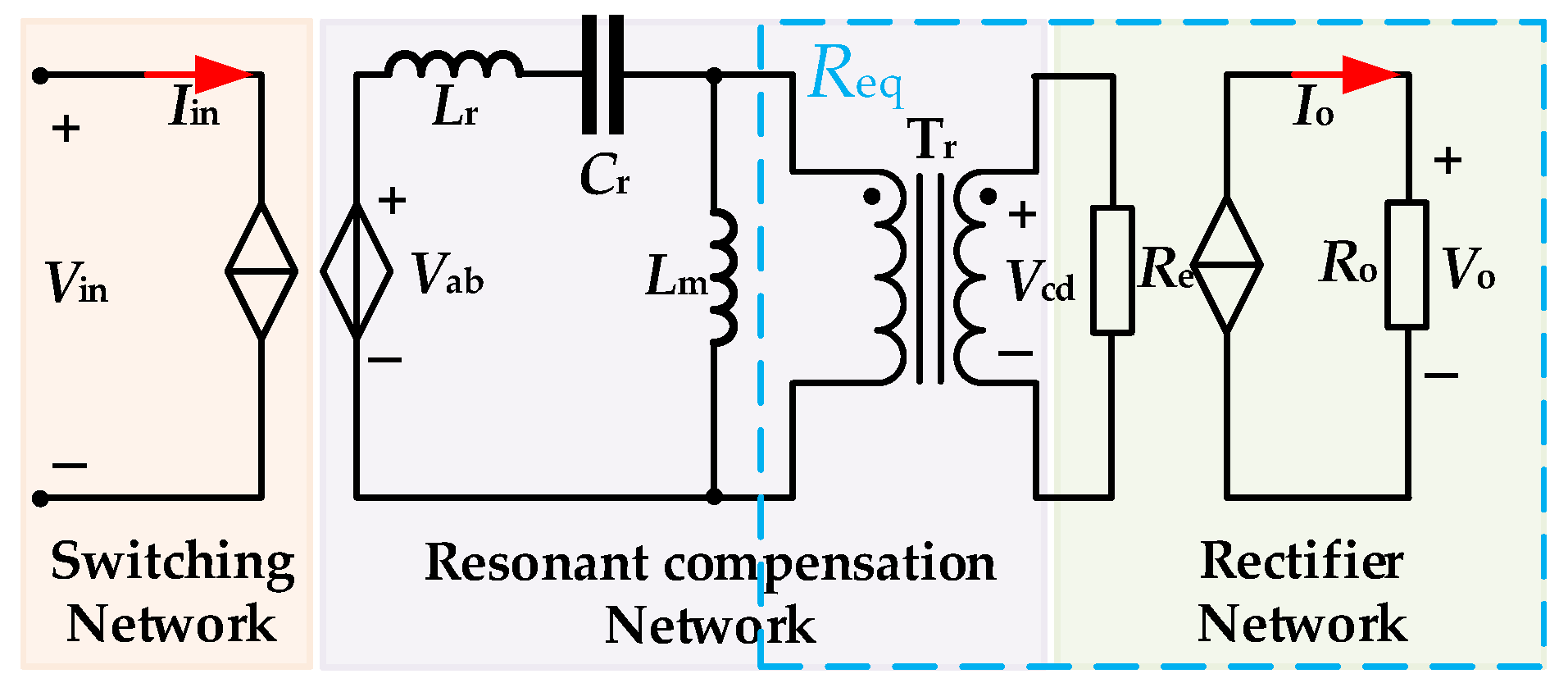
2. Operation Analysis of the Power Conversion System
2.1. Frequency Domain Analysis of LLC Circuits
2.2. Time Domain Analysis of LLC Circuits
- When the system is at the rated operating point, the increases in K value and Q value contribute to the increase of the system efficiency.
- When the system is out of the rated operating point, too large a K value will reduce the adjustment range of the switching frequency. It will not be conducive to the design of the control circuit and will cause the system to lose stability. When Q is too large, the system may enter the capacitive working region during the frequency regulation process. This is not conducive to the implementation of ZVS. What is more, it is difficult to achieve the high voltage gain of the system when the Q is too large.
- K and Q that are too large will also increase the current of the circuit and improve the voltage stress of the resonant element. This is not conducive to the selection of component models.
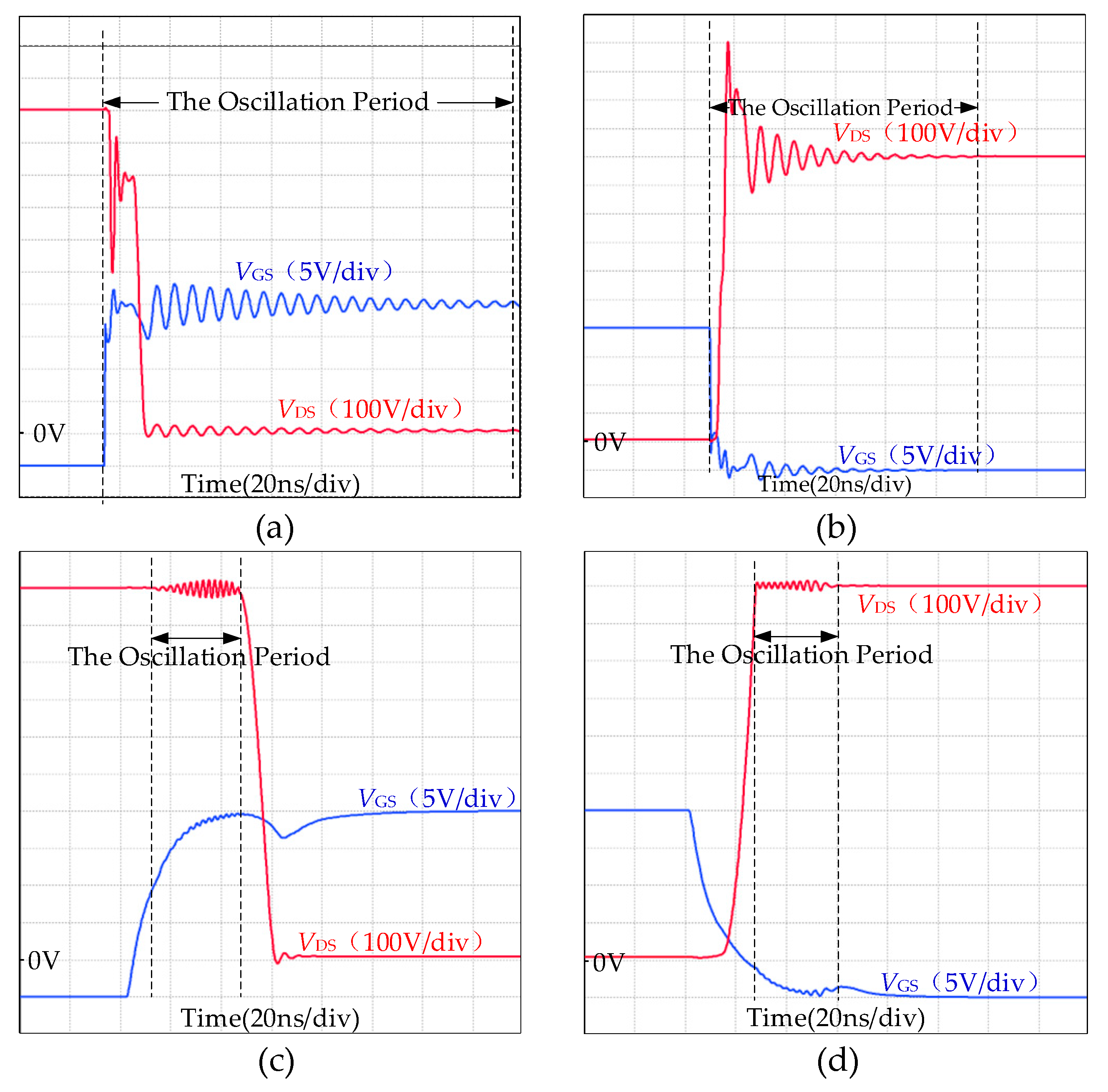
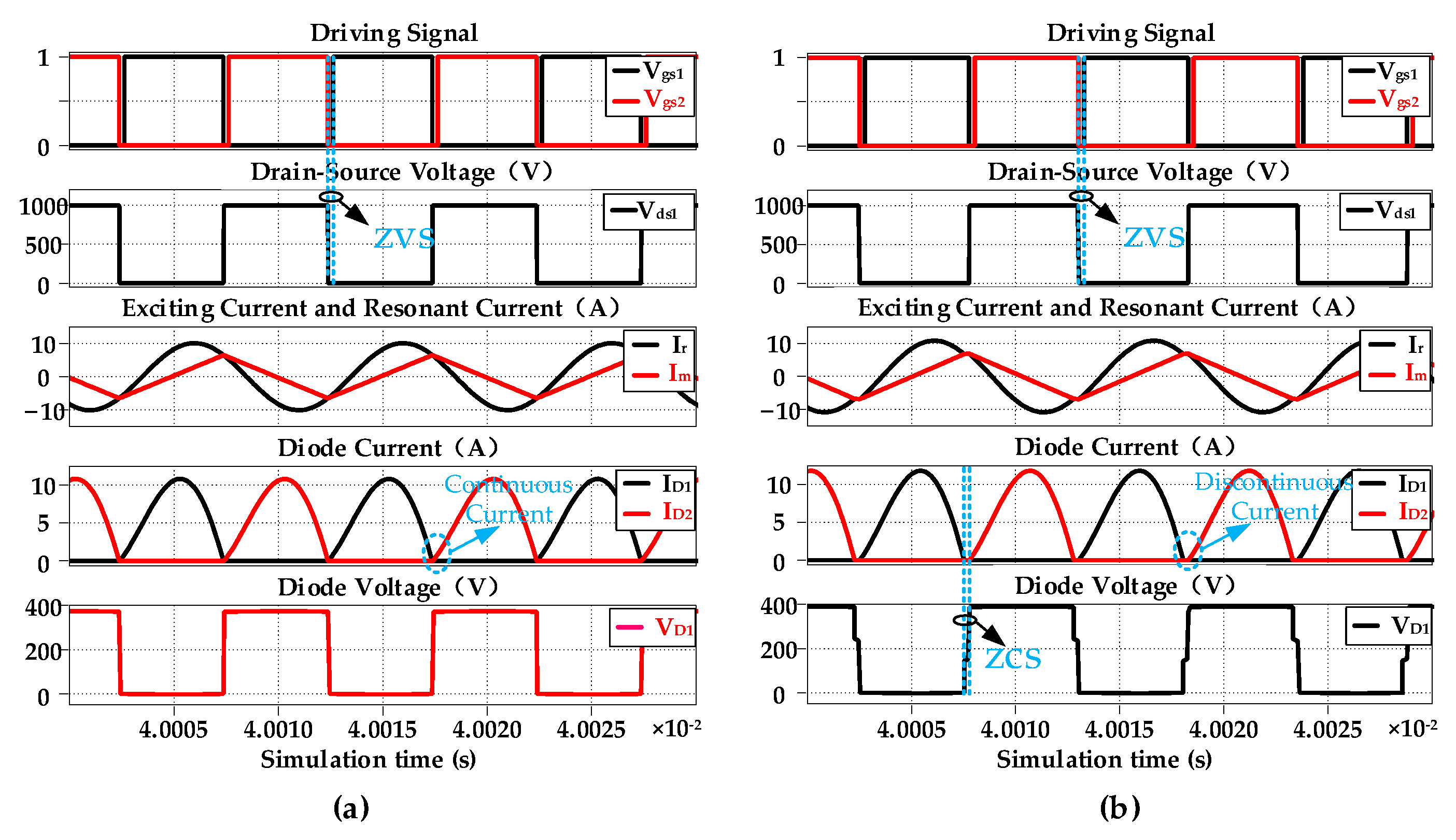
2.3. ZVS Characteristic Analysis
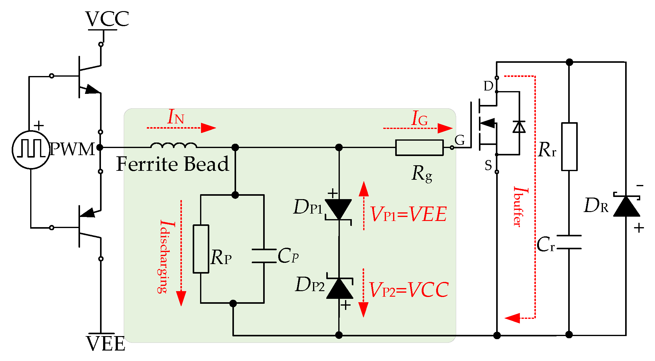
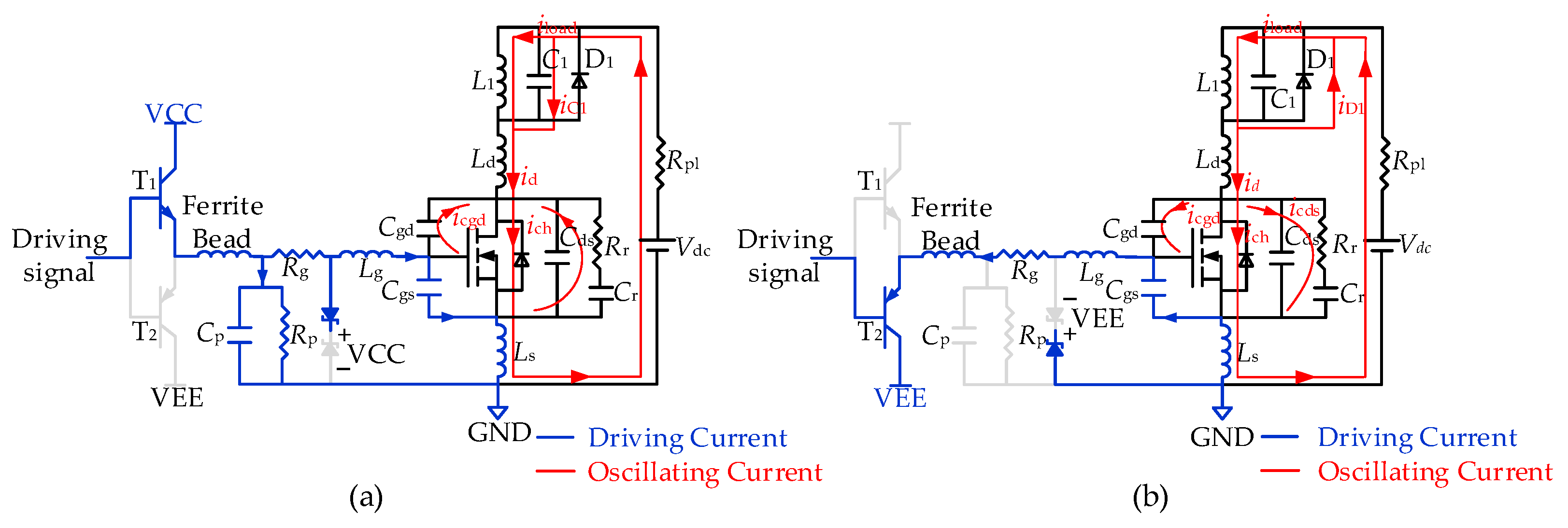
3. Optimization Design of Driving Circuit
3.1. Gate Circuit Design
3.2. Shift Circuit Design
3.3. RC Buffer Circuit Design
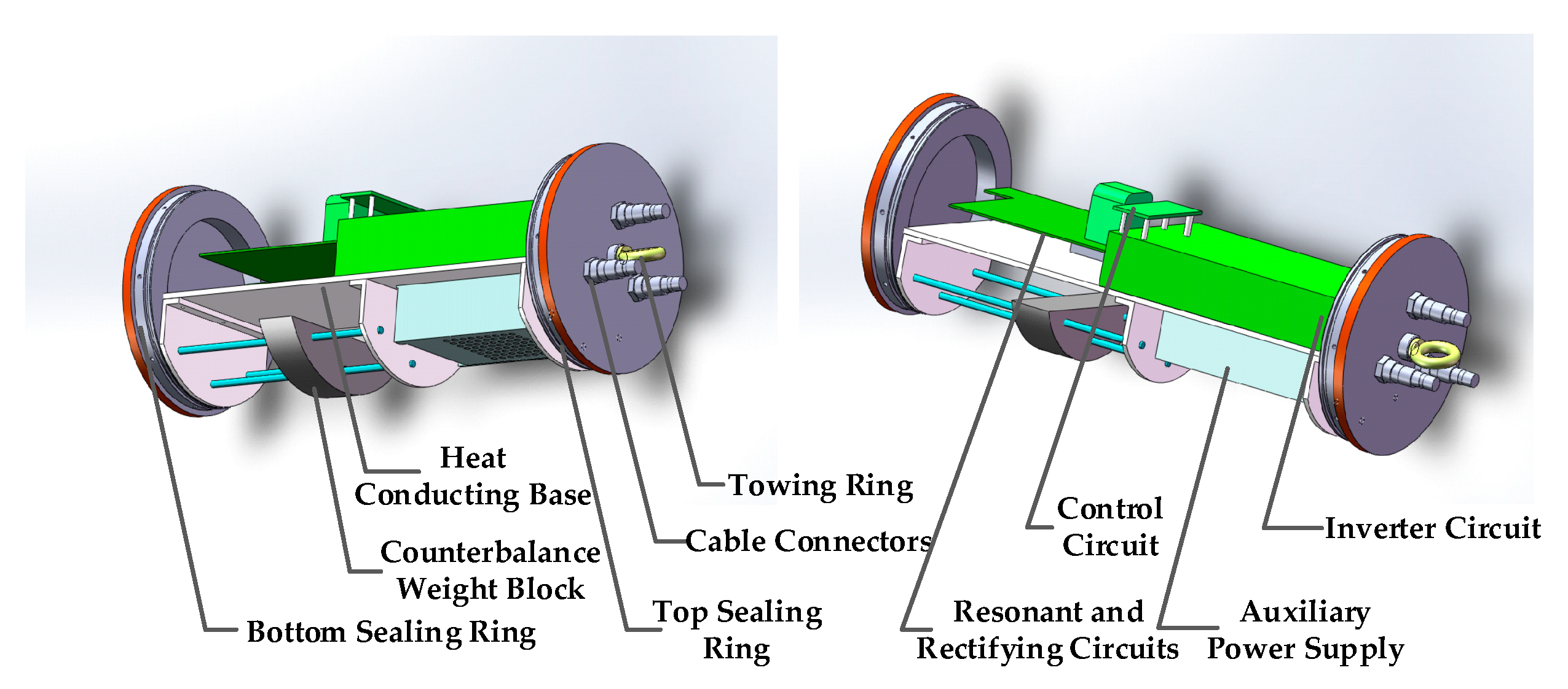
4. Circuit Design for Underwater Power Conversion Connector System
- (1)
- The value of the excitation inductor Lm needs to be calculated. The first resonant frequency of the system is 100 kHz. According to Equation (8), the relationship between the excitation inductor Lm and the system current can be established. As shown in Figure 6a, when the resonant current is less than 5 A, the critical value of the excitation inductor Lm is 384 µH.
- (2)
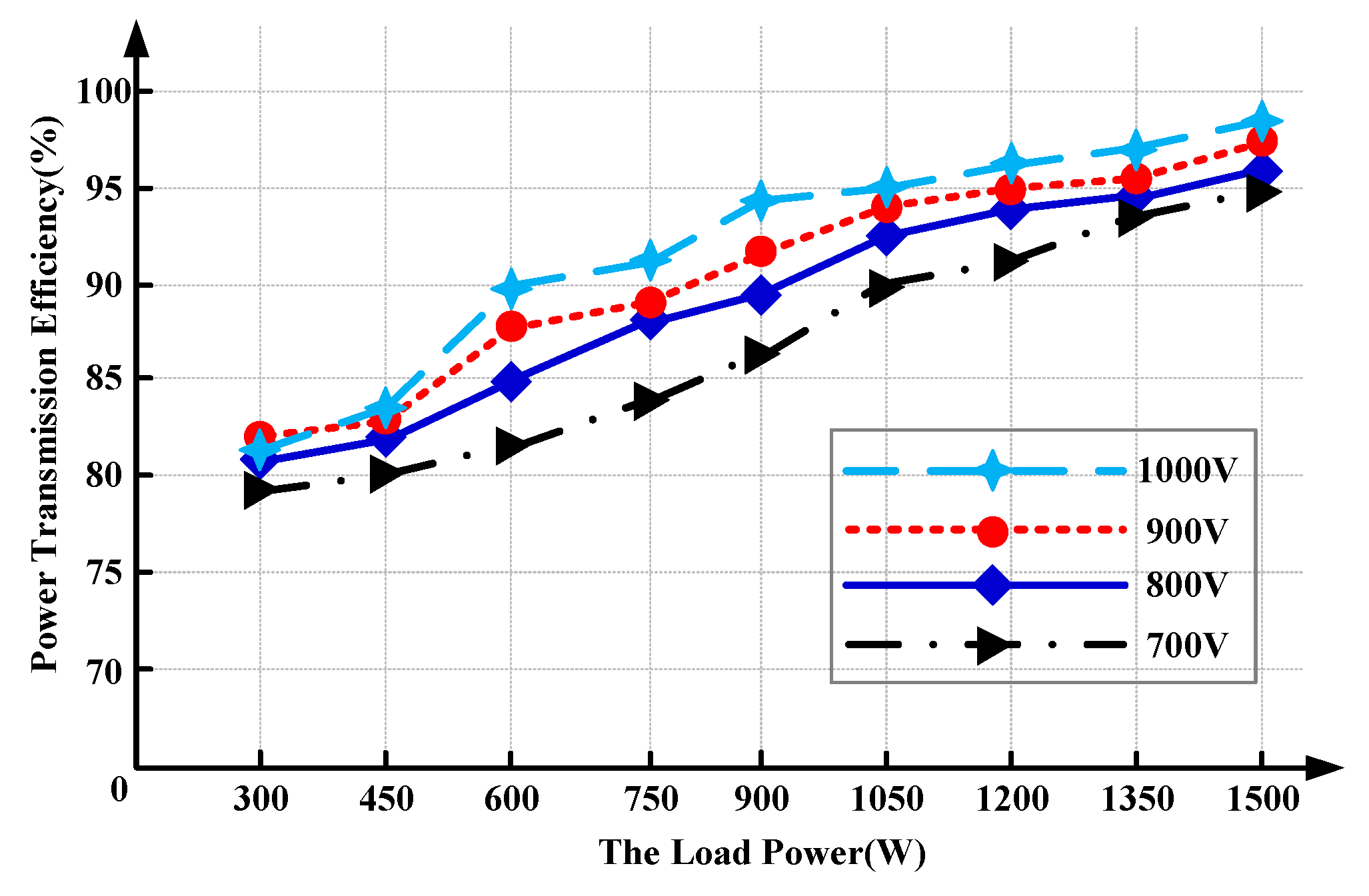
- K and Q need to be selected. The effect of K and Q on the system efficiency is shown in Figure 7. When the value of Lm is 384 μH, the relationship between K and Q is shown as the red curve. In addition, to achieve the high efficiency of the system, K and Q should be designed in the area above the blue curve. According to Figure 7b, the critical K and Q values are set as (5.3, 0.6), respectively.
- (3)
- The parameters of the power circuit that need to be designed. According to Equations (3) and (6), the values of the resonant capacitance Cr and the resonant inductance Lr are determined. In addition, according to Equation (11), the voltage stress of the system is shown in Figure 6b. The maximum voltage stress of the resonant capacitor Cr is 653 V, and the minimum is 480 V. The maximum voltage stress of the resonant inductance Lr is 316 V, and the minimum value is 311 V. Inductors and capacitors need to be connected in parallel or in series to meet the stress requirements.
- (4)
- The model of MOSFET selected in the paper is SCT20N170. Furthermore, the optical coupler is the ACPL-332J-500E, and it has a maximum propagation delay of 250 ns. According to the datasheet of MOSFET, the parasitic capacitance and the drive parameters are shown in Table 3.
- (5)
- Based on the driving circuit design theory presented in Section 3, the gate ferrite bead BLM18PG121SN1D is selected to suppress the oscillations during the turn-on and turn-off processes. At the same time, when the input voltage is 1000 V, the expected maximum voltage oscillation is 1200 V. According to Equations (32) and (33), the parameters of the driver circuit and power circuit are shown in Table 4.
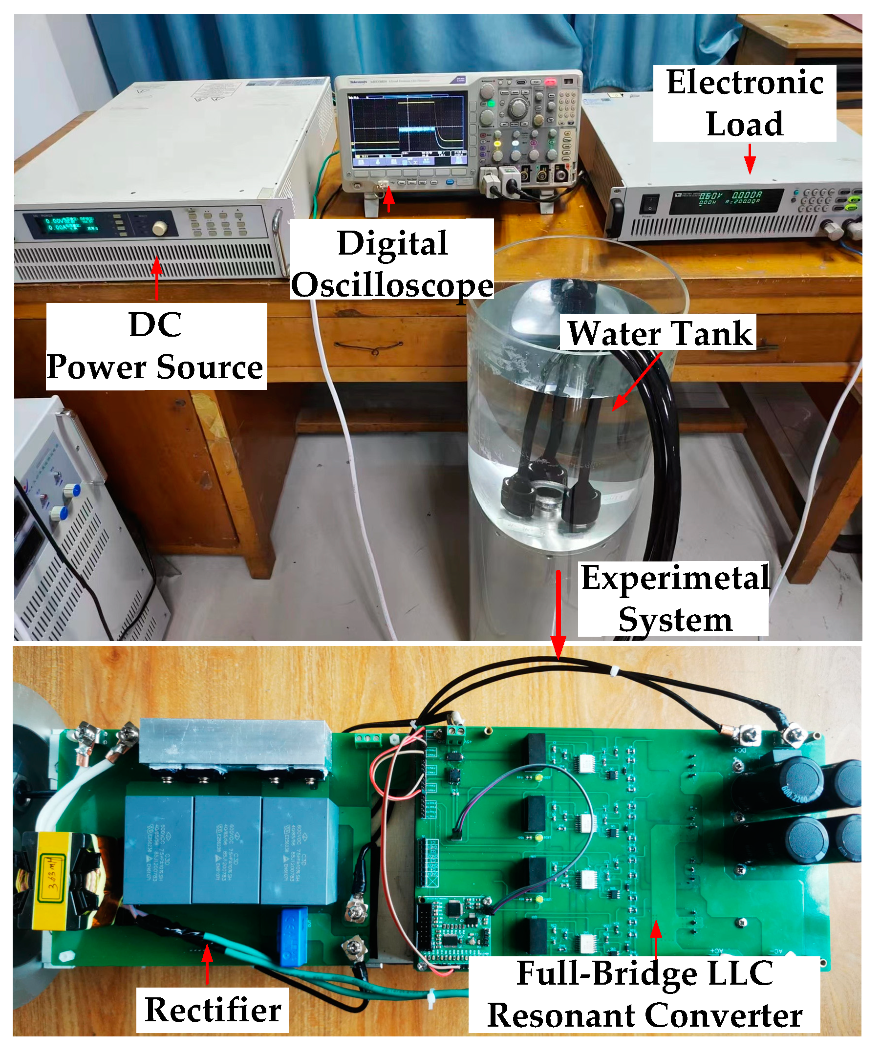
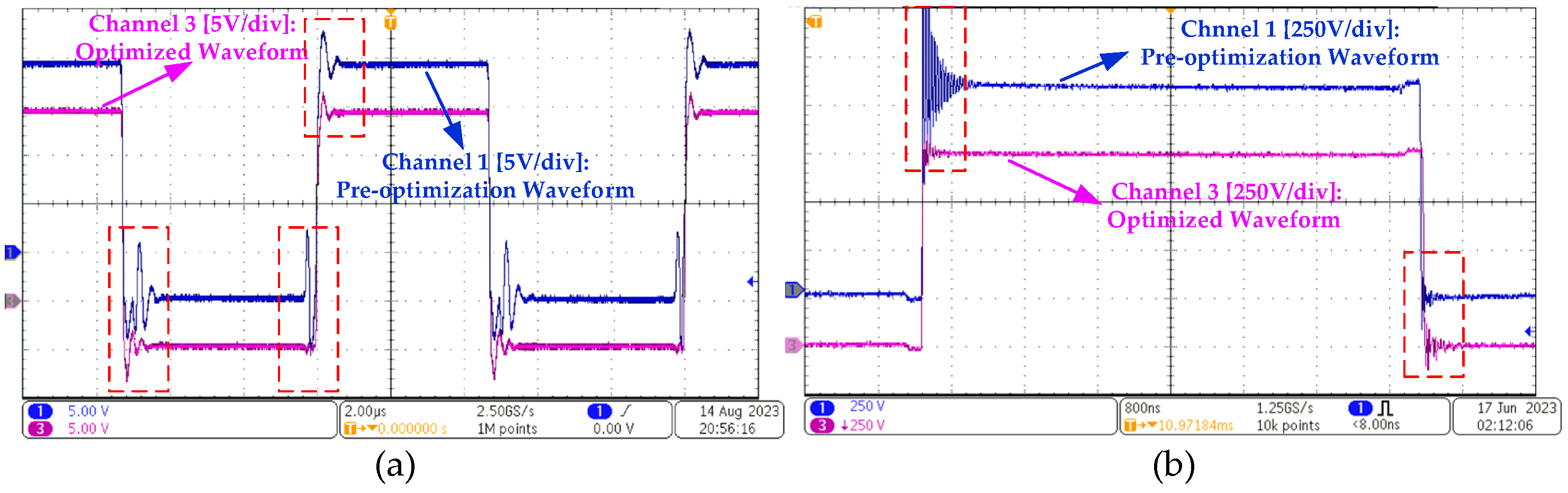
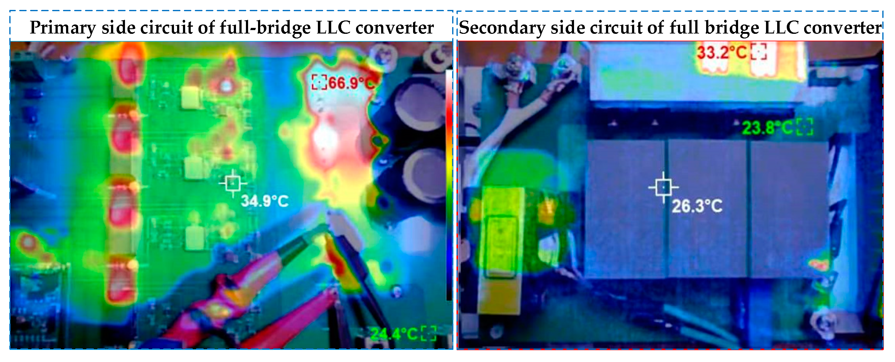
5. Simulated and Experimental Verification
6. Conclusions and Discussion
- Combined with fundamental wave analysis and time domain analysis, the parameters designing of the power circuit of the LLC converter are optimized, and the stress of the components is reduced.
- The characteristics of the zero-voltage switching (ZVS) were analyzed, and a dead zone time design based on the critical ZVS was analyzed. The stability and efficiency of the system are guaranteed by an appropriate dead zone time.
- The passive driving structure is proposed. It is conducive to improving the high-frequency performance of transistors. Therefore, a lot of switching losses during switching process could be avoided.
- A 1.5 kW prototype is developed, and an experimental platform is built. The experimental results show that the system structure and parameter configuration method are feasible.
Author Contributions
Funding
Institutional Review Board Statement
Informed Consent Statement
Data Availability Statement
Conflicts of Interest
Abbreviations
| Lg | Gate parasitic inductance of MOSFET. |
| Ld | Drain parasitic inductance of MOSFET. |
| Ls | Source parasitic inductance of MOSFET. |
| L1 | Load inductance. |
| Rpl | Bus equivalent resistance. |
| Vdc | Bus voltage. |
| Cgs | Grid-source parasitic capacitance of MOSFET. |
| Cds | Drain-source parasitic capacitance of MOSFET. |
| Cgd | Grid-drain parasitic capacitance of MOSFET. |
| C1 | Complementary bridge arm parasitic capacitance. |
References
- Liang, G.; Zhao, X.; Zhao, J.; Zhou, F. MVCNN: A Deep Learning-Based Ocean–Land Waveform Classification Network for Single-Wavelength LiDAR Bathymetry. IEEE J. Sel. Top. Appl. Earth Obs. Remote Sens. 2023, 16, 656–674. [Google Scholar] [CrossRef]
- Cai, T.; Lyu, F.; Wang, T.; Huang, F. Design of a Highly Compatible Underwater Wireless Power Transfer Station for Seafloor Observation Equipment. J. Mar. Sci. Eng. 2023, 11, 1205. [Google Scholar] [CrossRef]
- MahmoudZadeh, S.; Yazdani, A. A Cooperative Fault-Tolerant Mission Planner System for Unmanned Surface Vehicles in Ocean Sensor Network Monitoring and Inspection. IEEE Trans. Veh. Technol. 2023, 72, 1101–1115. [Google Scholar] [CrossRef]
- Gu, N.; Wang, D.; Peng, Z.; Wang, J.; Han, Q.-L. Advances in Line-of-Sight Guidance for Path Following of Autonomous Marine Vehicles: An Overview. IEEE Trans. Syst. Man Cybern. Syst. 2023, 53, 12–28. [Google Scholar] [CrossRef]
- Teeneti, C.; Truscott, T.; Beal, D.; Pantic, Z. Review of Wireless Charging Systems for Autonomous Underwater Vehicles. IEEE J. Ocean. Eng. 2019, 46, 68–87. [Google Scholar] [CrossRef]
- Liang, H.; Li, H.; Gao, J.; Cui, R.; Xu, D. Economic MPC-Based Planning for Marine Vehicles: Tuning Safety and Energy Efficiency. IEEE Trans. Ind. Electron. 2023, 70, 10546–10556. [Google Scholar] [CrossRef]
- Wang, Y.; Li, T.; Zeng, M.; Mai, J.; Gu, P.; Xu, D. An Underwater Simultaneous Wireless Power and Data Transfer System for AUV With High-Rate Full-Duplex Communication. IEEE Trans. Power Electron. 2022, 38, 619–633. [Google Scholar] [CrossRef]
- Xia, T.; Zhang, X.; Zhu, Z.; Yu, H.; Li, H. An Adaptive Control Strategy for Underwater Wireless Charging System Output Power with an Arc-Shaped Magnetic Core Structure. J. Mar. Sci. Eng. 2023, 11, 294. [Google Scholar] [CrossRef]
- Hu, A.P.; Dai, F.; Zhang, F.; Zhang, K.; Li, X.; Mao, Z.; Yan, Z. Analysis of Power Transfer Characteristics of IPT System With Near Field Magnetic Coupling. IEEE Trans. Electromagn. Compat. 2023, 65, 890–899. [Google Scholar] [CrossRef]
- Hasaba, R.; Yamaguchi, S.; Yagi, T.; Eguchi, K.; Satoh, H.; Koyanagi, Y.; Ura, T. Experimental Study of kW-Class Wireless Charging System for Autonomous Underwater Vehicle with Magnetic Resonance. In Proceedings of the 2023 IEEE Underwater Technology (UT), Tokyo, Japan, 6–9 March 2023; IEEE: Tokyo, Japan, 2023; pp. 1–4. [Google Scholar]
- Zeng, Y.; Lu, C.; Liu, R.; He, X.; Rong, C.; Liu, M. Wireless Power and Data Transfer System Using Multidirectional Magnetic Coupler for Swarm AUVs. IEEE Trans. Power Electron. 2023, 38, 1440–1444. [Google Scholar] [CrossRef]
- Mototani, S.; Yamamoto, R.; Doki, K.; Torii, A. Effect of Angle Offset of the Power Receiving Coil in Underwater Wireless Power Transfer Using a Cone Spiral Coil. In Proceedings of the 2022 International Power Electronics Conference (IPEC-Himeji 2022- ECCE Asia), Himeji, Japan, 15–19 May 2022; IEEE: Himeji, Japan, 2022; pp. 167–174. [Google Scholar]
- Yang, L.; Huang, J.; Feng, B.; Zhang, F.; Zhang, Y.; Li, X.; Jian, J.; Wang, Z.; Tong, X. Undersea Wireless Power and Data Transfer System With Shared Channel Powered by Marine Renewable Energy System. IEEE J. Emerg. Sel. Top. Circuits Syst. 2022, 12, 242–250. [Google Scholar] [CrossRef]
- Bagchi, A.C.; Saha, T.; Kamineni, A.; Zane, R. Analysis and Design of a Wireless Charger for Underwater Vehicles Fed from a Constant Current Distribution Cable. In Proceedings of the 2018 IEEE 19th Workshop on Control and Modeling for Power Electronics (COMPEL), Padua, Italy, 25–28 June 2018; IEEE: Padua, Italy, 2018; pp. 1–8. [Google Scholar]
- Yang, L.; Ma, L.; Huang, J.; Fu, Y. Characteristics of Undersea Capacitive Wireless Power Transfer System. In Proceedings of the 2020 IEEE 9th International Power Electronics and Motion Control Conference (IPEMC2020-ECCE Asia), Nanjing, China, 29 November 2020; IEEE: Nanjing, China, 2020; pp. 2952–2955. [Google Scholar]
- Li, H.; Li, G.; Jin, X.; Li, J.; Xu, G. A LC-CLL Compensated Capacitive Wireless Power Transfer System in Fresh Water. In Proceedings of the 2022 5th International Conference on Power and Energy Applications (ICPEA), Guangzhou, China, 18 November 2022; IEEE: Guangzhou, China, 2022; pp. 130–137. [Google Scholar]
- Le, H.N.; Tedeschi, E. Comparative Evaluation of AC and DC Power Distribution Systems for Underwater Vehicles Based on Multiobjective Optimization Techniques. IEEE Trans. Power Deliv. 2021, 36, 3456–3465. [Google Scholar] [CrossRef]
- Wang, S.; Wang, Z.; Liu, X.; Ye, X. An SOC-Based Bidirectional Virtual DC Machine Control for Energy Storage Systems in Offshore Isolated Island DC Microgrids. J. Mar. Sci. Eng. 2023, 11, 1502. [Google Scholar] [CrossRef]
- Lu, F.; Zhou, H.; Yue, J.; Peng, X.; He, B.; Wu, Z. Design of an Undersea Power System for the East China Sea Experimental Cabled Seafloor Observatory. In Proceedings of the 2013 OCEANS, San Diego, CA, USA, 23–27 September 2013; pp. 1–6. [Google Scholar]
- Saha, T.; Bagchi, A.C.; Wang, H.; Zane, R. Analysis and Design of Wide Range Output Voltage Regulated Power Supply for Underwater Constant Input Current DC Distribution System. In Proceedings of the 2018 IEEE 19th Workshop on Control and Modeling for Power Electronics (COMPEL), 25–28 June 2018; IEEE: Padua, Italy, 2018; pp. 1–7. [Google Scholar]
- Saha, T.; Bagchi, A.C.; Zane, R.A. Analysis and Design of an LCL–T Resonant DC–DC Converter for Underwater Power Supply. IEEE Trans. Power Electron. 2021, 36, 6725–6737. [Google Scholar] [CrossRef]
- Saha, T.; Wang, H.; Riar, B.; Zane, R. Analysis and Design of a Parallel Resonant Converter for Constant Current Input to Constant Voltage Output DC-DC Converter Over Wide Load Range. In Proceedings of the 2018 International Power Electronics Conference (IPEC-Niigata 2018 -ECCE Asia), Niigata, Japan, 20–24 May 2018; IEEE: Niigata, Japan, 2018; pp. 4074–4079. [Google Scholar]
- Saha, T.; Bagchi, A.C.; Wang, H.; Zane, R.A. Bidirectional LCL-T Resonant DC–DC Converter for Priority Loads in Undersea Distribution Networks. IEEE Trans. Power Electron. 2022, 37, 14874–14887. [Google Scholar] [CrossRef]
- Saha, T.; Bagchi, A.C.; Zane, R. Time-Domain Analysis and ZVS Assistance Design for a DAB LCL-T Resonant Converter in Underwater DC Current Distribution Network. In Proceedings of the 2020 IEEE 21st Workshop on Control and Modeling for Power Electronics (COMPEL), Aalborg, Denmark, 9 November 2020; IEEE: Aalborg, Denmark, 2020; pp. 1–7. [Google Scholar]
- Han, X.; Yao, X.; Liao, Y. Full Operating Range Optimization Design Method of LLC Resonant Converter in Marine DC Power Supply System. J. Mar. Sci. Eng. 2023, 11, 2142. [Google Scholar] [CrossRef]
- Diekhans, T.; De Doncker, R.W. A Dual-Side Controlled Inductive Power Transfer System Optimized for Large Coupling Factor Variations and Partial Load. IEEE Trans. Power Electron. 2015, 30, 6320–6328. [Google Scholar] [CrossRef]
- Ivensky, G.; Bronshtein, S.; Abramovitz, A. Approximate Analysis of Resonant LLC DC-DC Converter. IEEE Trans. Power Electron. 2011, 26, 3274–3284. [Google Scholar] [CrossRef]
- Xu, H.; Yin, Z.; Zhao, Y.; Huang, Y. Accurate Design of High-Efficiency LLC Resonant Converter With Wide Output Voltage. IEEE Access 2017, 5, 26653–26665. [Google Scholar] [CrossRef]
- Wei, Y.; Luo, Q.; Wang, Z.; Mantooth, H.A. A Complete Step-by-Step Optimal Design for LLC Resonant Converter. IEEE Trans. Power Electron. 2021, 36, 3674–3691. [Google Scholar] [CrossRef]
- Wu, H.; Wang, X.; Ortiz-Gonzalez, J.; Alatise, O.; Pickert, V. Investigation into the Switching Transient of SiC MOSFET Using Voltage/Current Source Gate Driver. In Proceedings of the 10th International Conference on Power Electronics, Machines and Drives (PEMD 2020), Online Conference, 15–17 December 2020; Institution of Engineering and Technology; pp. 657–662. [Google Scholar]
- the Institute for Power Electronics and Electrical Drives, RWTH Aachen University; Engelmann, G. Experimental Investigation on the Transient Switching Behavior of SiC MOSFETs Using a Stage-Wise Gate Driver. CPSS TPEA 2018, 3, 77–87. [Google Scholar] [CrossRef]
- Li, Y.; Liang, M.; Chen, J.; Zheng, T.Q.; Guo, H. A Low Gate Turn-OFF Impedance Driver for Suppressing Crosstalk of SiC MOSFET Based on Different Discrete Packages. IEEE J. Emerg. Sel. Top. Power Electron. 2019, 7, 353–365. [Google Scholar] [CrossRef]
- Chen, J.; Luo, Q.; Huang, J.; He, Q.; Sun, P.; Du, X. Analysis and Design of an RC Snubber Circuit to Suppress False Triggering Oscillation for GaN Devices in Half-Bridge Circuits. IEEE Trans. Power Electron. 2020, 35, 2690–2704. [Google Scholar] [CrossRef]
- Tang, H.-T.; Shu-Hung Chung, H.; Wing-To Fan, J.; Shun-Cheung Yeung, R.; Wing-Hong Lau, R. Passive Resonant Level Shifter for Suppression of Crosstalk Effect and Reduction of Body Diode Loss of SiC MOSFETs in Bridge Legs. IEEE Trans. Power Electron. 2020, 35, 7204–7225. [Google Scholar] [CrossRef]
- Li, H.; Qiu, Z.; Du, H.; Shao, T. Research on Active Gate Driver for Improving Turn-off Performance and Gate Voltage Stability of SiC MOSFET in Bridge Circuit. Proc. CSEE 2022, 42, 7922–7934. [Google Scholar]
- Yang, C. Technologies of Junction Box for Seafloor Observation Network. JME 2015, 51, 172. [Google Scholar] [CrossRef]


| Reference | Type of Topology | Power Level | Output Voltage | Soft Switching | Switching Frequency | Efficiency |
|---|---|---|---|---|---|---|
| [20] | LLC resonant | / | 380 V | Nope | 106 kHz | / |
| [21] | Parallel resonant | 450 W | 120 V | ZVS | 250 kHz | / |
| [22] | LCL–T resonant | 500 W | 150 V | ZVS | 250 kHz | 96.0% |
| [23] | Parallel resonant | 500 W | 50~250 V | ZVS | 250 kHz | 94.0% |
| [24] | DAB | 500 W | 150 V | ZVS | 250 kHz | 95.0% |
| [25] | LLC resonant | 200 W | 60 V | ZVS/ZCS | 100 kHz | 93.2% |
| This Work | LLC resonant | 1500 W | 375 V | ZVS/ZCS | 100 kHz | 98.0% |
| Reference | [32] | [33] | [34] | [35] |
|---|---|---|---|---|
| Feature | Dual Capacitance | Passive RC Resonant | RCD Level Shift | Active Current Injection |
| Driver Structure | 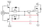 | 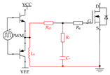 | 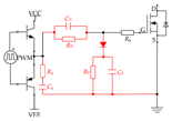 | 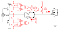 |
| Advantages | Low turn-off gate impedance | Small oscillation of drive voltage | Stable turn-on or turn-off state | Small transient drive voltage and current |
| Disadvantages | Turn-off time delay increased | High drain-source voltage | Causes higher order oscillations | Complex circuit and driving loss is large |
| Test Conditions | In the 1.1 kW buck converter | Double pulse test | In the 1 kW full-bridge inverter | Double pulse test |
| Type of Device | C3M0065090X | EPC2015 | C3M0065090J | CMF20120D |
| Frequency | 100 kHz | 200 kHz | 145 kHz | 100 kHz |
| Conclusion | System efficiency is improved by 0.60% | Oscillation amplitude is reduced by 61.00% | Switching loss is improved by 24.9% | The peak of the drain current is reduced by 19.50% |
| Symbol | Parameter | Value | Unit |
|---|---|---|---|
| VDS | Drain-source voltage | 1000 | V |
| VGS | Gate-source voltage | −5/+20 | V |
| ID | Drain current (25 °C to 100 °C) | 5 | A |
| Ciss | Input capacitance | 1568 | pF |
| Coss | Output capacitance | 141 | pF |
| Crss | Reverse transfer capacitance | 21 | pF |
| td | Dead zone time of driving | 127–302 | ns |
| Symbol | Parameter | Value | Unit |
|---|---|---|---|
| Drive Circuit Specifications | |||
| Rg | Gate resistance | 7.85 | Ω |
| RP | Shift circuit resistance | 4 | kΩ |
| CP | Shift circuit capacitance | 513 | nF |
| Rs | Buffer circuit resistance | 83 | mΩ |
| Cs | Buffer circuit capacitance | 15 | pF |
| Resonant Circuit Specifications | |||
| n | Turns ratio of the transformer | 8/3 | |
| Lr | Resonant inductance | 72.45 | µH |
| Cr | Resonant capacitance | 23 | nF |
| Lm | Magnetic inductance | 384 | µH |
Disclaimer/Publisher’s Note: The statements, opinions and data contained in all publications are solely those of the individual author(s) and contributor(s) and not of MDPI and/or the editor(s). MDPI and/or the editor(s) disclaim responsibility for any injury to people or property resulting from any ideas, methods, instructions or products referred to in the content. |
© 2024 by the authors. Licensee MDPI, Basel, Switzerland. This article is an open access article distributed under the terms and conditions of the Creative Commons Attribution (CC BY) license (https://creativecommons.org/licenses/by/4.0/).
Share and Cite
Yang, L.; Chen, X.; Zhang, Y.; Feng, B.; Wen, H.; Yang, T.; Zhao, X.; Huang, J.; Zhu, D.; Zhao, Y.; et al. Underwater Power Conversion and Junction Technology for Underwater Wireless Power Transfer Stations. J. Mar. Sci. Eng. 2024, 12, 561. https://doi.org/10.3390/jmse12040561
Yang L, Chen X, Zhang Y, Feng B, Wen H, Yang T, Zhao X, Huang J, Zhu D, Zhao Y, et al. Underwater Power Conversion and Junction Technology for Underwater Wireless Power Transfer Stations. Journal of Marine Science and Engineering. 2024; 12(4):561. https://doi.org/10.3390/jmse12040561
Chicago/Turabian StyleYang, Lei, Xinze Chen, Yuanqi Zhang, Baoxiang Feng, Haibing Wen, Ting Yang, Xin Zhao, Jingjing Huang, Darui Zhu, Yaopeng Zhao, and et al. 2024. "Underwater Power Conversion and Junction Technology for Underwater Wireless Power Transfer Stations" Journal of Marine Science and Engineering 12, no. 4: 561. https://doi.org/10.3390/jmse12040561
APA StyleYang, L., Chen, X., Zhang, Y., Feng, B., Wen, H., Yang, T., Zhao, X., Huang, J., Zhu, D., Zhao, Y., Zhang, A., & Tong, X. (2024). Underwater Power Conversion and Junction Technology for Underwater Wireless Power Transfer Stations. Journal of Marine Science and Engineering, 12(4), 561. https://doi.org/10.3390/jmse12040561