A Comparative Study on the Effects of Passivation Methods on the Carrier Lifetime of RIE and MACE Silicon Micropillars


Abstract
:1. Introduction
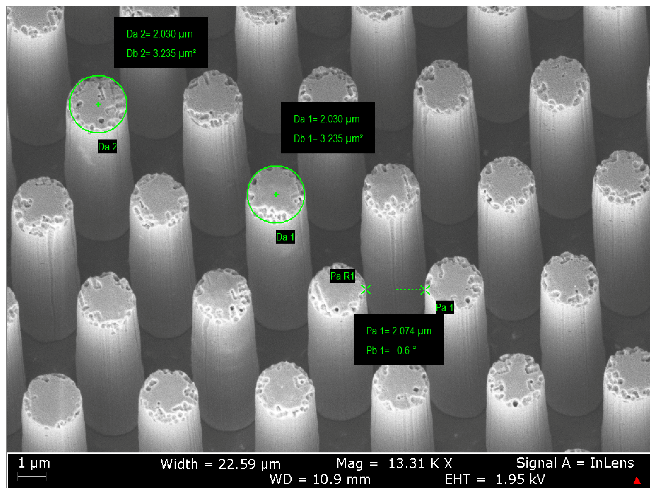
2. Materials and Methods
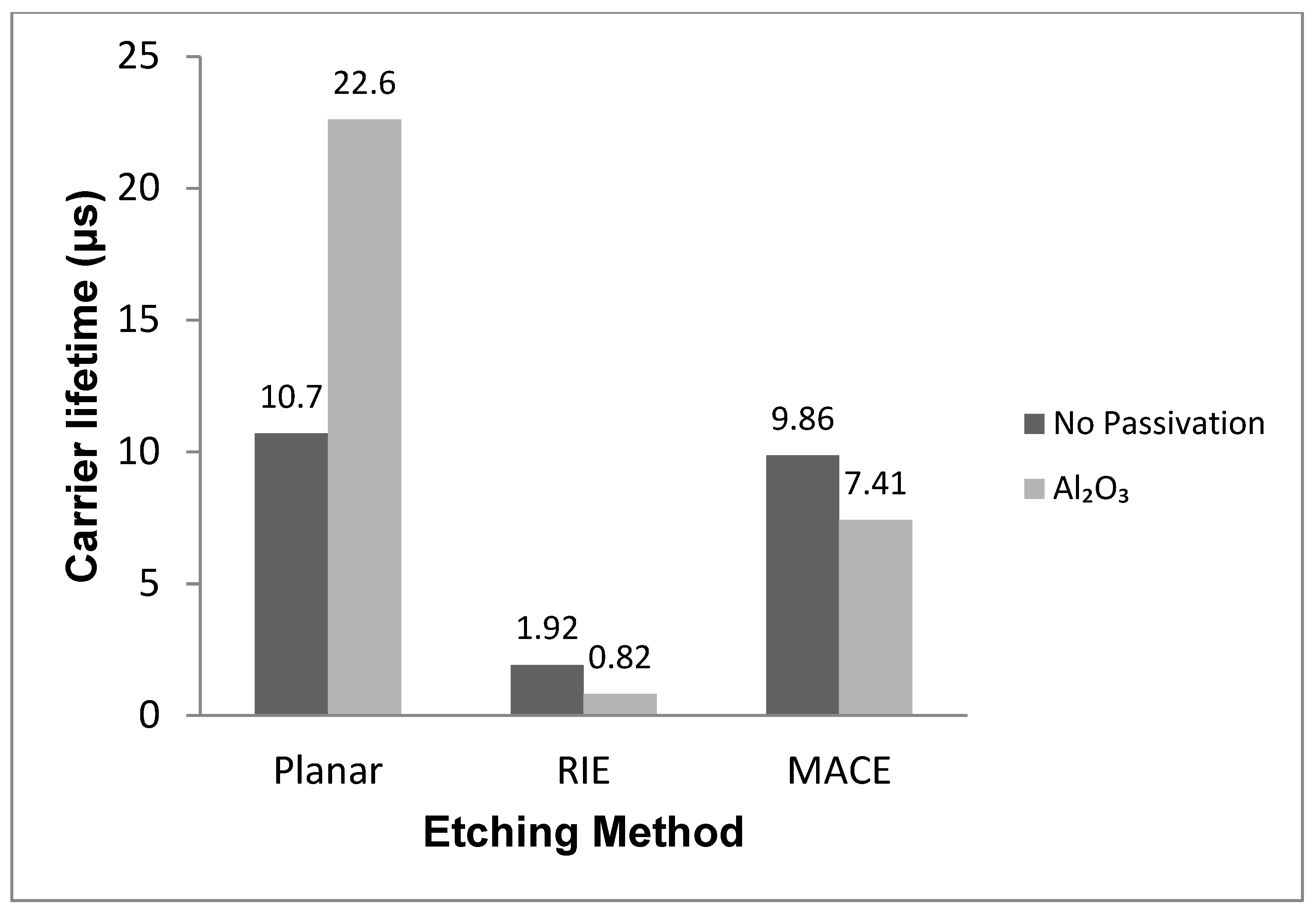
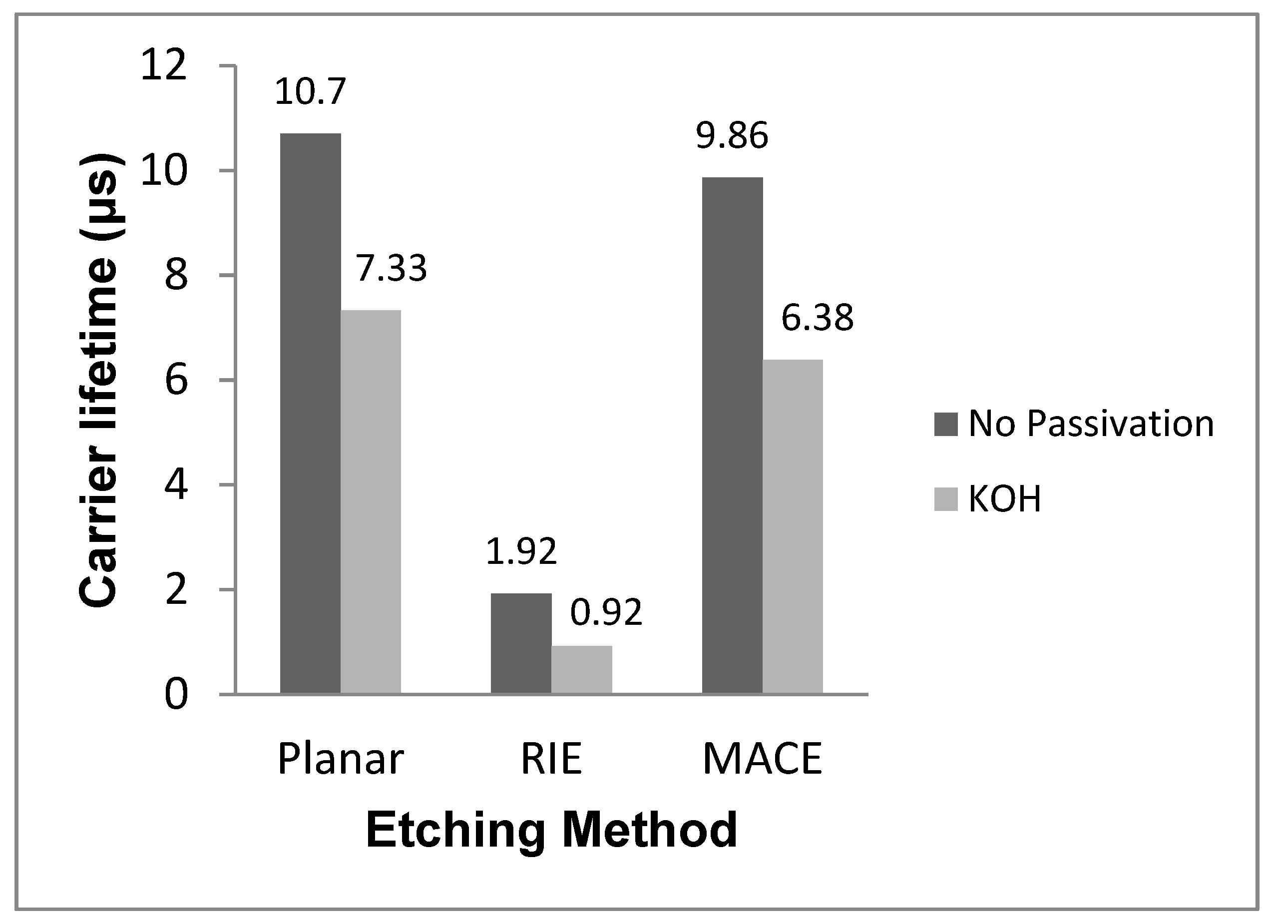
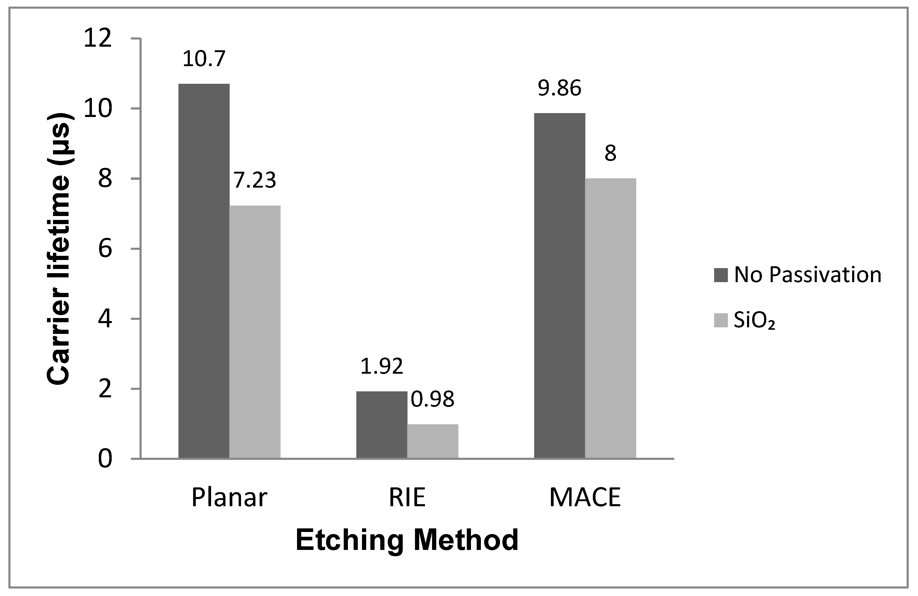
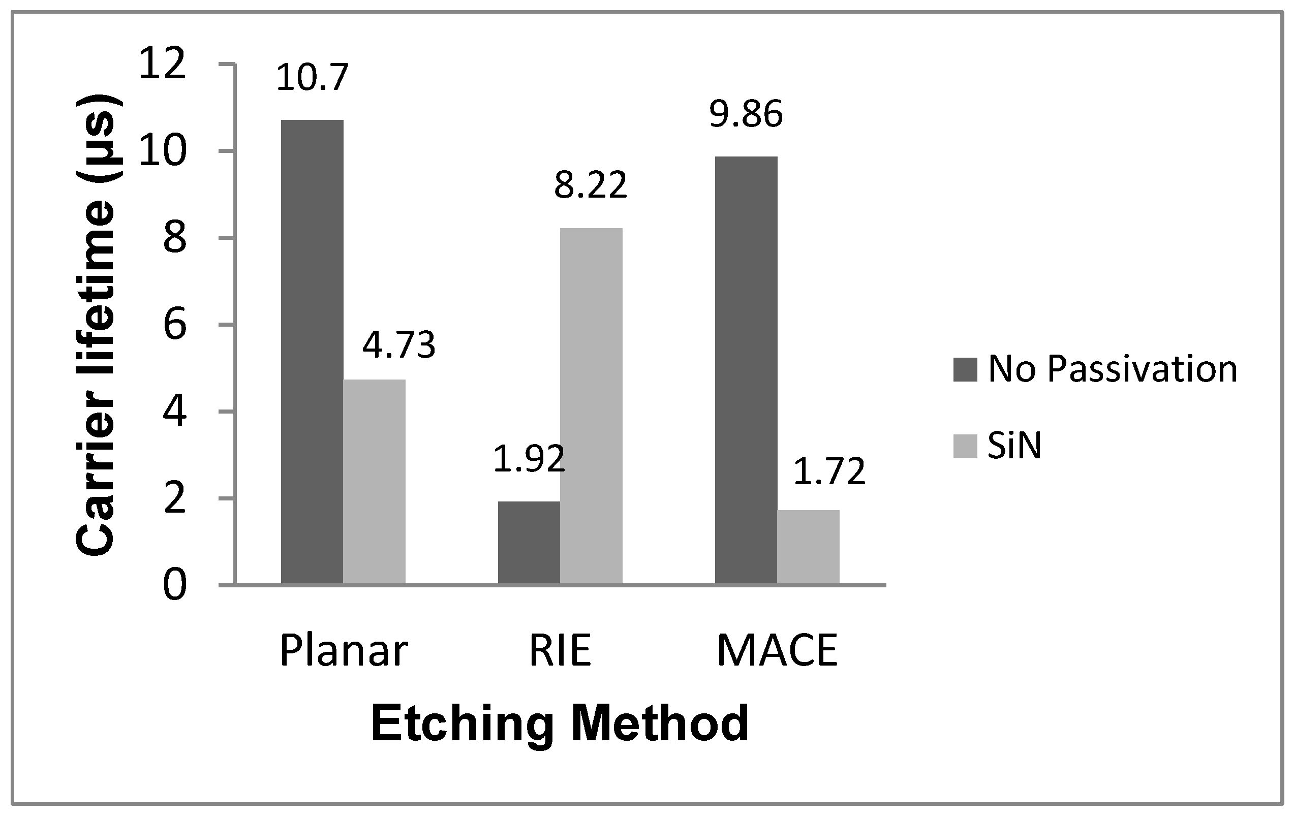
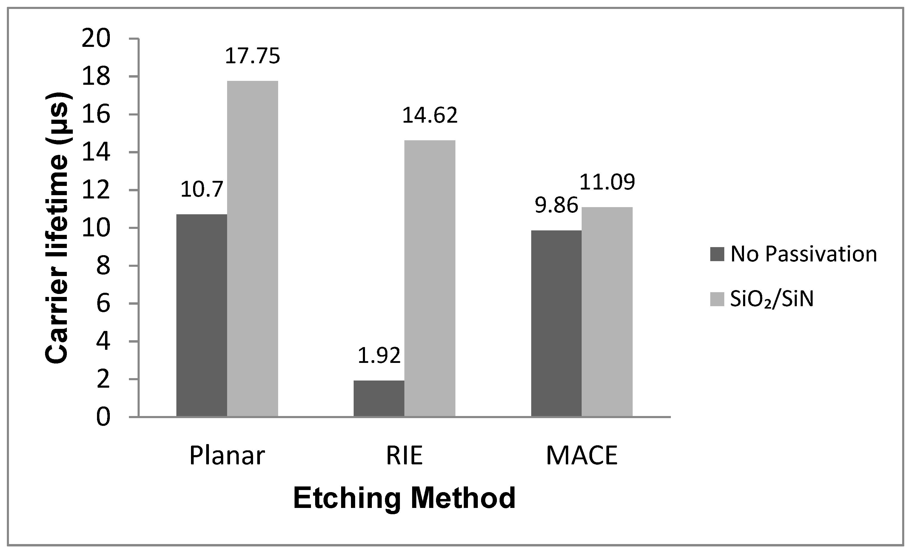
3. Results
4. Discussion
5. Conclusions
Funding
Conflicts of Interest
References
- Yoon, H.P.; Yumen, Y.A.; Shen, H.; Podraza, N.J.; Mallouk, T.E.; Dickey, E.C.; Redwing, J.A.; Wronski, C.R.; Mayer, T.S. Parametric study of micropillar array solar cells. In Proceedings of the 37th IEEE Photovoltaic Specialists Conference, Seattle, WA, USA, 19–24 April 2011; pp. 000303–000306. [Google Scholar] [CrossRef]
- Shieh, J.; You, C.Y.; Liu, J.M.; Chiu, C.C. Improving optical and electrical properties of micropillar and black-Si solar cells by combining them into a superstructure. In Proceedings of the 23rd International Workshop on Active-Matrix Flatpanel Displays and Devices (AM-FPD), Kyoto, Japan, 6–8 July 2016; pp. 222–224. [Google Scholar] [CrossRef]
- Ha, J.; Lee, S.W.; Lee, H.-J.; Lee, H.-J.; Lee, S.H.; Goto, H.; Kato, T.; Fujii, K.; Cho, M.W.; Yao, T. The fabrication of vertical light-emitting diodes using chemical lift-off process. IEEE Photonics Technol. Lett. 2008, 20, 175–177. [Google Scholar] [CrossRef]
- Conway, A.M.; Wang, T.F.; Deo, N.; Cheung, C.L.; Nikolic, R.J. Numerical simulations of pillar structured solid state thermal neutron detector: Efficiency and gamma discrimination. IEEE Trans. Nucl. Sci. 2009, 56, 2802–2807. [Google Scholar] [CrossRef]
- Gerasopoulos, K.; Pomerantseva, E.; McCarthy, M.; Culver, J.; Wang, C.; Ghodssi, R. A hierarchical approach for the fabrication of three-dimensional microbattery electrodes. In Proceedings of the 2011 16th International Solid-State Sensors, Actuators and Microsystems Conference, Beijing, China, 5–9 June 2011; pp. 727–730. [Google Scholar] [CrossRef]
- Tsakalakos, L.; Balch, J.; Fronheiser, J.; Korevaar, B.A.; Sulima, O. Silicon nanowire solar cells. Appl. Phys. Lett. 2007, 91, 233117. [Google Scholar] [CrossRef]
- Muskens, O.L.; Rivas, J.G.; Algra, R.E.; Bakkers, E.P.; Lagendijk, A. Design of light scattering in nanowire materials for photovoltaic applications. Nano Lett. 2008, 8, 2638–2642. [Google Scholar] [CrossRef]
- Zhu, J.; Yu, Z.; Burkhard, G.F.; Hsu, C.M.; Connor, S.T.; Xu, Y.; Wang, Q.; McGehee, M.D.; Fan, S.; Cui, Y. Optical absorption enhancement in amorphous silicon nanowire and nanocone arrays. Nano Lett. 2009, 9, 279–282. [Google Scholar] [CrossRef] [PubMed]
- Kelzenberg, M.D.; Boettcher, S.W.; Petykiewicz, J.A.; Turner-Evans, D.B.; Putnam, M.C.; Warren, E.L.; Spurgeon, J.M.; Briggs, R.M.; Lewis, N.S.; Atwater, H.A. Enhanced absorption and carrier collection in si wire arrays for photovoltaic applications. Nat. Mater. 2010, 14, 239–244. [Google Scholar] [CrossRef]
- Zhu, J.; Hsu, C.M.; Yu, Z.; Fan, S.; Cui, Y. Nanodome solar cells with efficienct light management and self-cleaning. Nano Lett. 2010, 10, 1979–1984. [Google Scholar] [CrossRef] [PubMed]
- Gharghi, M.; Fathi, E.; Kante, B.; Sivoththaman, S.; Zhang, X. Heterojunction silicon microwire solar cells. Nano Lett. 2012, 12, 6278–6282. [Google Scholar] [CrossRef]
- Park, W.I.; Zheng, G.; Jiang, X.; Tian, B.; Lieber, C.M. Controlled synthesis of millimeter-long silicon nanowires with uniform electronic properties. Nano Lett. 2008, 8, 3004–3009. [Google Scholar] [CrossRef]
- Xu, T.; Tao, Z.; Li, H.; Tan, X.; Li, H. Effects of deep reactive ion etching parameters on etching rate and surface morphology in extremely deep silicon etch process with high aspect ratio. Adv. Mech. Eng. 2017, 9, 1–12. [Google Scholar] [CrossRef]
- Liu, S.; Niu, X.; Shan, W.; Lu, W.; Zheng, J.; Li, Y.; Duan, H.; Quan, W.; Han, W.; Wronski, C.R.; Yang, D. Improvement of conversion efficiency of multicrystalline silicon solar cells by incorporating reactive ion etching texturing. Sol. Energy Mater. Sol. Cells 2014, 127, 21–26. [Google Scholar] [CrossRef]
- Qian, H.X.; Zhou, W.; Miao, J.; Lim, L.; Zeng, X.R. Fabrication of Si microstructures using focused ion beam implantation and reactive ion etching. J. Micromech. Microeng. 2008, 18, 035003. [Google Scholar] [CrossRef]
- Miller, K.; Li, M.; Walsh, K.M.; Fu, X. The effects of DRIE operational parameters on vertically aligned micropillar arrays. J. Micromech. Microeng. 2013, 23, 035039. [Google Scholar] [CrossRef]
- Li, X.; Xiao, Y.; Bang, J.; Lausch, D.; Meyer, S.; Miclea, P.; Jung, J.; Schweizer, S.; Lee, J.; Wehrspohn, R. Upgraded silicon nanowires by metal-assited etching of metallurgical silicon: A new route to nanostructured solar-grade silicon. Adv. Mater. 2013, 25, 3187–3191. [Google Scholar] [CrossRef]
- Huang, Z.; Geyer, N.; Werner, P.; Boor, J.; Gosele, U. Metal-assisted chemical etching of silicon: A review. Adv. Mater. 2011, 23, 285–308. [Google Scholar] [CrossRef] [PubMed]
- Henry, M.; Walavalkar, S.; Homyk, A.; Scherer, A. Alumina etch masks for fabrication of high-aspect-ratio silicon micropillars and nanopillars. Nanotechnology 2009, 20, 255305–255309. [Google Scholar] [CrossRef]
- Sainiemi, L.; Nissilä, T.; Jokinen, V.; Sikanen, T.; Kotiaho, T.; Kostiainen, R.; Ketola, R.; Franssila, S. Fabrication and fluidic characterization of silicon micropillar array electrospray ionization chip. Sens. Actuators B 2018, 132, 380–387. [Google Scholar] [CrossRef]
- Kilchenmann, S.; Rollo, E.; Bianchi, E.; Guiducci, C. Metal-coated silicon micropillars for freestanding 3D-electrode arrays in microchannels. Sens. Actuators B 2013, 185, 713–719. [Google Scholar] [CrossRef]
- Shin, J.C.; Chanda, D.; Chern, W.; Yu, K.; Rogers, J. Experimental study of design parameters in silicon micropillar array solar cells produced by soft lithography and metal-assisted chemical etching. IEEE J. Photovoltaics 2012, 2, 129–133. [Google Scholar] [CrossRef]
- Li, X.; Bohn, W.P. Metal-assisted chemical etching in HF/H2O2 produces porous silicon. Appl. Phys. Lett. 2000, 77, 2572–2574. [Google Scholar] [CrossRef]
- Veeco Instruments. Savannah-Thermal ALD for R&D. Available online: http://www.cambridgenanotechald.com/products/Savannah-ald-system.shtml (accessed on 12 April 2019).
- Semilab Inc. µ-PCD Carrier Lifetime for Wafers. Available online: https://www.semilab.hu/category/products/u-pcd-carrier-lifetime-wafers (accessed on 12 April 2019).
- Lin, X.; Hua, X.; Huang, Z.; Shen, W. Realization of high performance silicon nanowire based solar cells with large size. Naotechnology 2013, 24, 235402–235410. [Google Scholar] [CrossRef] [PubMed]
- Oh, J.; Yuan, H.-C.; Branz, H.M. An 18.2%-efficiency black-silicon solar cell achieved through control of carrier recombination in nanostructures. Nat. Nano. 2012, 7, 743–748. [Google Scholar] [CrossRef] [PubMed]
- Toan, N.V.; Toda, M.; Ono, T. High aspect ratio silicon structures produced via metal assisted chemical etching and assembly technology for cantilever fabrication. IEEE Trans. Nanotechnol. 2017, 16, 567–573. [Google Scholar] [CrossRef]


| Planar | RIE | MACE | |
|---|---|---|---|
| Average Carrier Lifetime | 17.8 μs | 14.6 μs | 11.1 μs |
| Image | 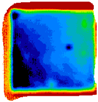 | 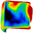 |  |
| Histogram |  | 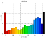 |  |
© 2019 by the author. Licensee MDPI, Basel, Switzerland. This article is an open access article distributed under the terms and conditions of the Creative Commons Attribution (CC BY) license (http://creativecommons.org/licenses/by/4.0/).
Share and Cite
Kabalan, A. A Comparative Study on the Effects of Passivation Methods on the Carrier Lifetime of RIE and MACE Silicon Micropillars. Appl. Sci. 2019, 9, 1804. https://doi.org/10.3390/app9091804
Kabalan A. A Comparative Study on the Effects of Passivation Methods on the Carrier Lifetime of RIE and MACE Silicon Micropillars. Applied Sciences. 2019; 9(9):1804. https://doi.org/10.3390/app9091804
Chicago/Turabian StyleKabalan, Amal. 2019. "A Comparative Study on the Effects of Passivation Methods on the Carrier Lifetime of RIE and MACE Silicon Micropillars" Applied Sciences 9, no. 9: 1804. https://doi.org/10.3390/app9091804
APA StyleKabalan, A. (2019). A Comparative Study on the Effects of Passivation Methods on the Carrier Lifetime of RIE and MACE Silicon Micropillars. Applied Sciences, 9(9), 1804. https://doi.org/10.3390/app9091804