Article

MOCVD Growth and Investigation of InGaN/GaN Heterostructure Grown on AlGaN/GaN-on-Si Template

1
International Center for Material Nanoarchitectonics (MANA), National Institute for Materials Science (NIMS), 1-1 Namiki, Tsukuba, Ibaraki 305-0044, Japan
2
Department of Information and Communications Engineering, Kogakuin University, 2665-1 Nakano, Hachioji, Tokyo 192-0015, Japan
3
Research Center for Functional Materials, National Institute for Materials Sciences, Namiki 1-1, Tsukuba, Ibaraki 305-0044, Japan
4
Amano-Koide Collaborative Research Lab, National Institute for Materials Science, (NIMS), 1-1 Namiki, Tsukuba, Ibaraki 305-0044, Japan
*
Author to whom correspondence should be addressed.
Appl. Sci. 2019, 9(9), 1746; https://doi.org/10.3390/app9091746
Submission received: 25 February 2019 / Revised: 21 April 2019 / Accepted: 22 April 2019 / Published: 27 April 2019
(This article belongs to the Special Issue III-V Nitride: Materials, Physics and Devices)

Abstract

:
The investigation of the III-V nitride-based driving circuits is in demand for the development of GaN-based power electronic devices. In this work, we aim to grow high-quality InGaN/GaN heterojunctions on the n-channel AlGaN/GaN-on-Si high electron mobility transistor (HEMT) templates to pursue the complementary p-channel conductivity to realize the monolithic integrated circuits. As the initial step, the epitaxial growth is optimized and the structure properties are investigated by comparing with the InGaN/GaN heterojunctions grown on GaN/sapphire templates. It is found that both the In composition and relaxation degree are higher for the InGaN/GaN on the HEMT template than that on the sapphire substrate. The crystalline quality is deteriorated for the InGaN grown on the HEMT template, which is attributed to the poor-quality GaN channel in the HEMT template. Further analysis indicates that the higher In incorporation in the InGaN layer on the HEMT template may be caused by the higher relaxation degree due to the compositional pulling effect. An increase in the growth temperature by 20 °C with optimized growth condition improves the crystalline quality of the InGaN, which is comparable to that on GaN/sapphire even if it is grown on a poor-quality GaN channel.

1. Introduction

The Si-based complementary logic integrated circuits (ICs) are showing the drawbacks of large leakage currents or poor reliabilities in harsh environments, especially for high-power applications. On the other hand, GaN-based field effect transistors (FETs) can achieve a much higher breakdown voltage and faster switching speed than Si FETs benefitting from their higher mobility at the heterojunctions, larger saturation velocity, higher breakdown voltages, and higher thermal and chemical stability [1,2,3]. To efficiently drive and control the GaN-based power electronic devices, the ultimate choice is to utilize one-chip CMOS logic circuits with both n-channel and p-channel FETs [4]. However, compared with the rapid development in the n-channel AlGaN/GaN high electron mobility transistors (HEMTs) using the two-dimensional electron gas (2DEG), little attention has been paid to the p-channel FETs with the two-dimensional hole gas (2DHG). Actually, the 2DHG channel in the AlGaN and AlInGaN-based heterostructures has been expected according to the polarization theory [5,6,7,8,9]. In the III-V nitride family, an InGaN/GaN heterojunction could offer a better route for the p-channel transistors compared to the AlGaN system in terms of a much lower on-resistance because of its lower activation energy of Mg and hole effective mass [10,11]. InGaN has the highest piezoelectric polarization coefficient among all the III-V nitride materials, which is beneficial for the generation of high-density 2DHG in the conducting channel [12]. More importantly, the utilization of InGaN/GaN p-channel structures can avoid the crack problem when grown on AlGaN/GaN n-channel transistors as a result of the in-plane compressive strain. In 2015, our group has successfully achieved 2DHG at the InGaN/GaN heterostructure on the sapphire substrate, and fabricated p-channel metal-oxide-semiconductor (MOS) FETs, which can be operated from cryogenic to room temperature [2]. To realize the CMOS circuits, it is better to deposit the p-channel transistors on the n-channel AlGaN/GaN template. In this regard, the AlGaN/GaN-on-Si HEMT template will be promising due to its lower cost and better integration with Si electronics. Unfortunately, as a result of the large lattice mismatch between AlGaN and InGaN, it is still difficult to obtain high-performance p-channel FETs on HEMT/Si structures. To achieve a high mobility and hole concentration, the high-quality InGaN/GaN heterojunction with a high crystalline quality and good interface is necessary to avoid the dislocation and alloy disorder scattering. Therefore, the optimization in the epitaxial growth and the property investigation of InGaN/GaN on the HEMT/Si template is necessary and in great demand.
In this work, we systematically investigate and analyze the growth, and structural and optical properties of InGaN/GaN heterostructures grown on the commercial AlGaN/GaN-on-Si HEMT templates by comparing with those grown on the GaN/sapphire templates. It is found that the strain state and indium incorporation in the heterojunctions are quite different even if they are grown at the same conditions. The crystalline quality of the InGaN/GaN heterojunction is dependent on the quality of the templates. The optimization on the growth condition can improve the interface and crystalline quality of the InGaN/GaN heterojunction.

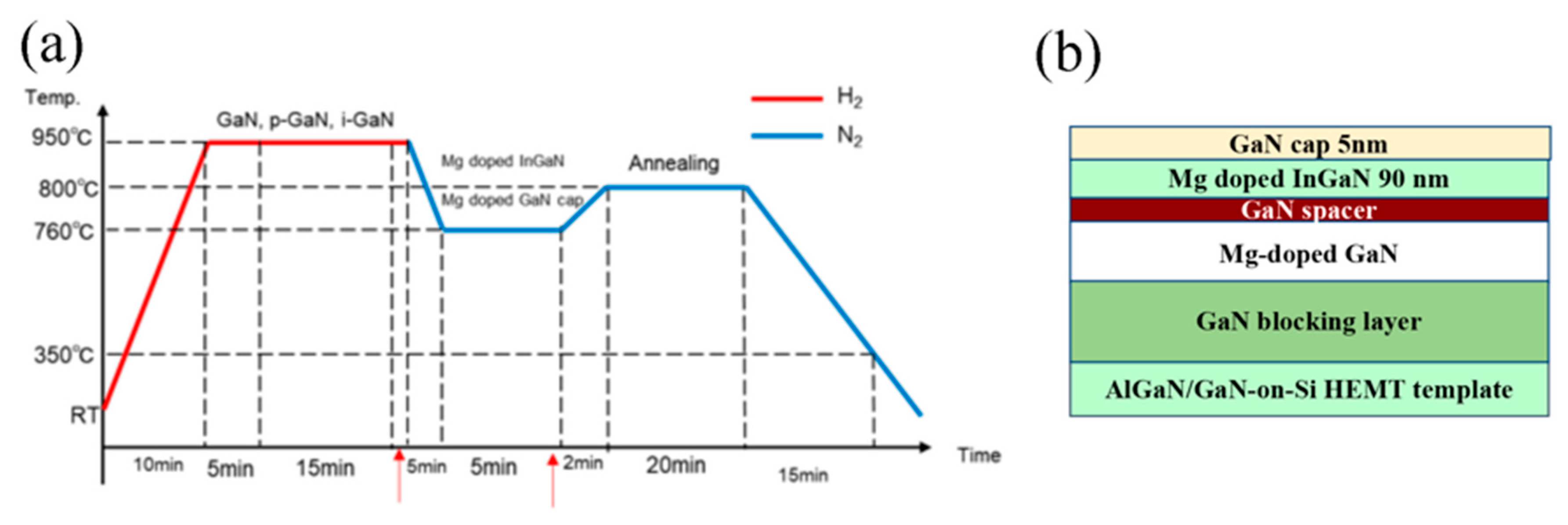
2. Experimental Details

The InGaN/GaN heterostructures were deposited on commercial AlGaN/GaN-on-Si HEMT templates (provided by Enkris Semiconductor, Inc., Suzhou, China) by using the metal-organic chemical vapor deposition (MOCVD). Trimethylgallium (TMG), trimethylindium (TMI), and ammonia served as the precursors, and nitrogen as the carrier gas. The process of MOCVD deposition is schematically shown in Figure 1a. Figure 1b is the structure of InGaN/GaN heterojuntion on the HEMT template. The thickness of Mg-doped InGaN and GaN were 90 nm and 1 µm, respectively, which were simulated for the maximum piezoelectric field. A thin unintentionally doped GaN spacer layer with the thickness of 5 nm was introduced before the InGaN deposition. Then a 20-min growth interruption in both nitrogen and ammonia ambient was introduced to polish the interface. The growth interruption can improve the interface quality, which was confirmed in our previous studies [13,14]. Finally, a 5-nm-thick GaN cap layer was introduced to improve the surface morphology and screen the surface trap effects. During the InGaN deposition, a low Mg doping was performed to compensate the n-type background concentration. The growth temperature of the InGaN layers was varied from 760 to 780 °C. The InGaN/GaN heterostructure was also deposited on the GaN/sapphire template at the same growth condition as the reference. The crystalline qualities and strain states of the epitaxial structures were characterized by high-resolution X-ray diffraction (XRD) and reciprocal space mapping (RSM) using Panalytical Xpert PRO XRD system. All XRD peaks were calibrated using the standard peak of the bulk substrate (sapphire or Si). The photoluminescence (PL) measurement was carried out at room temperature with a He–Cd laser excited micro-photoluminescence system at 325 nm.

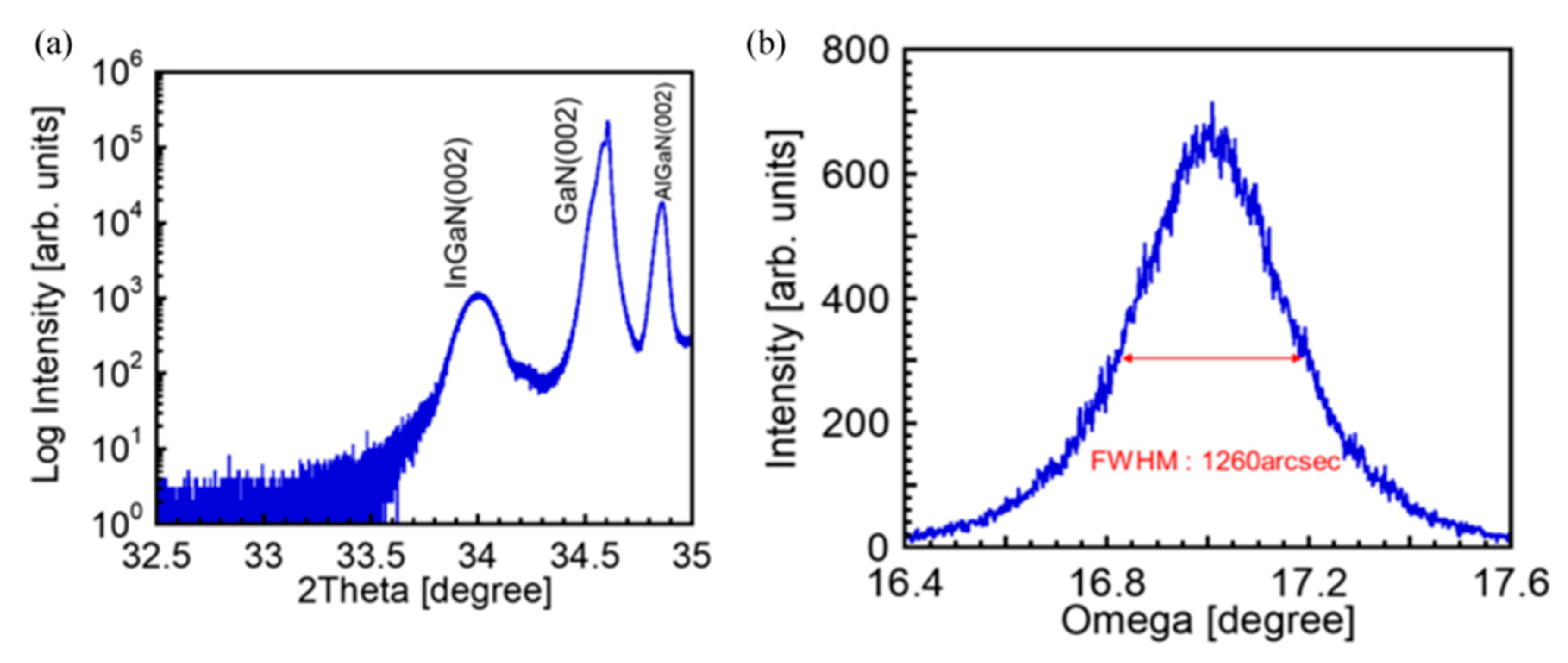
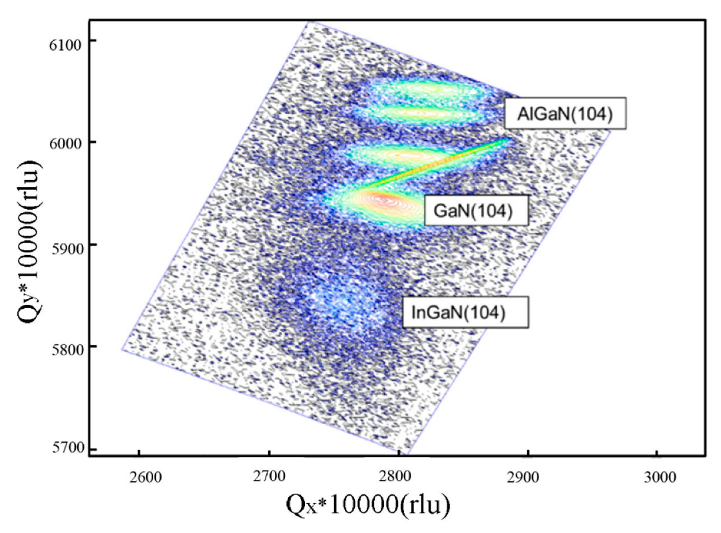
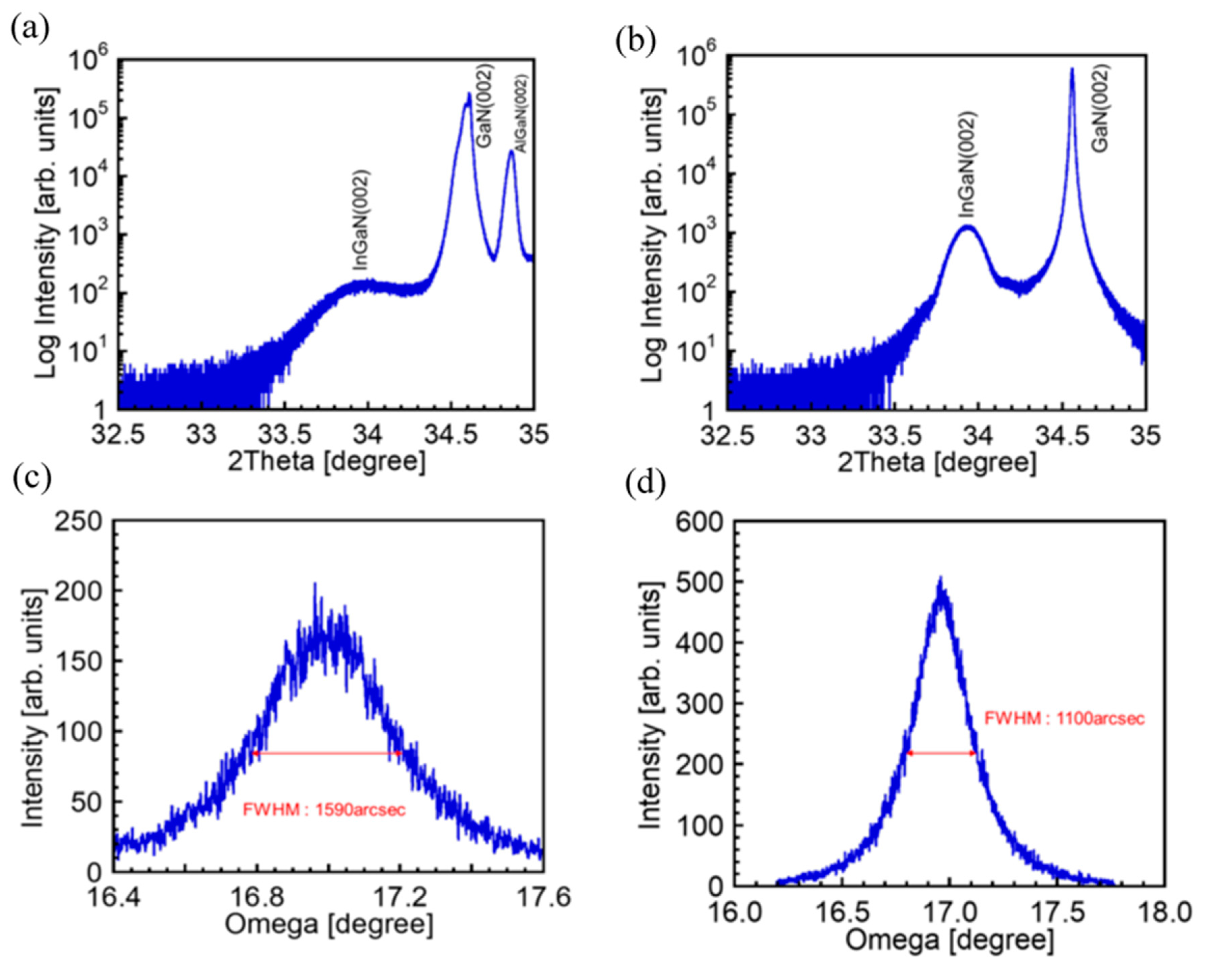
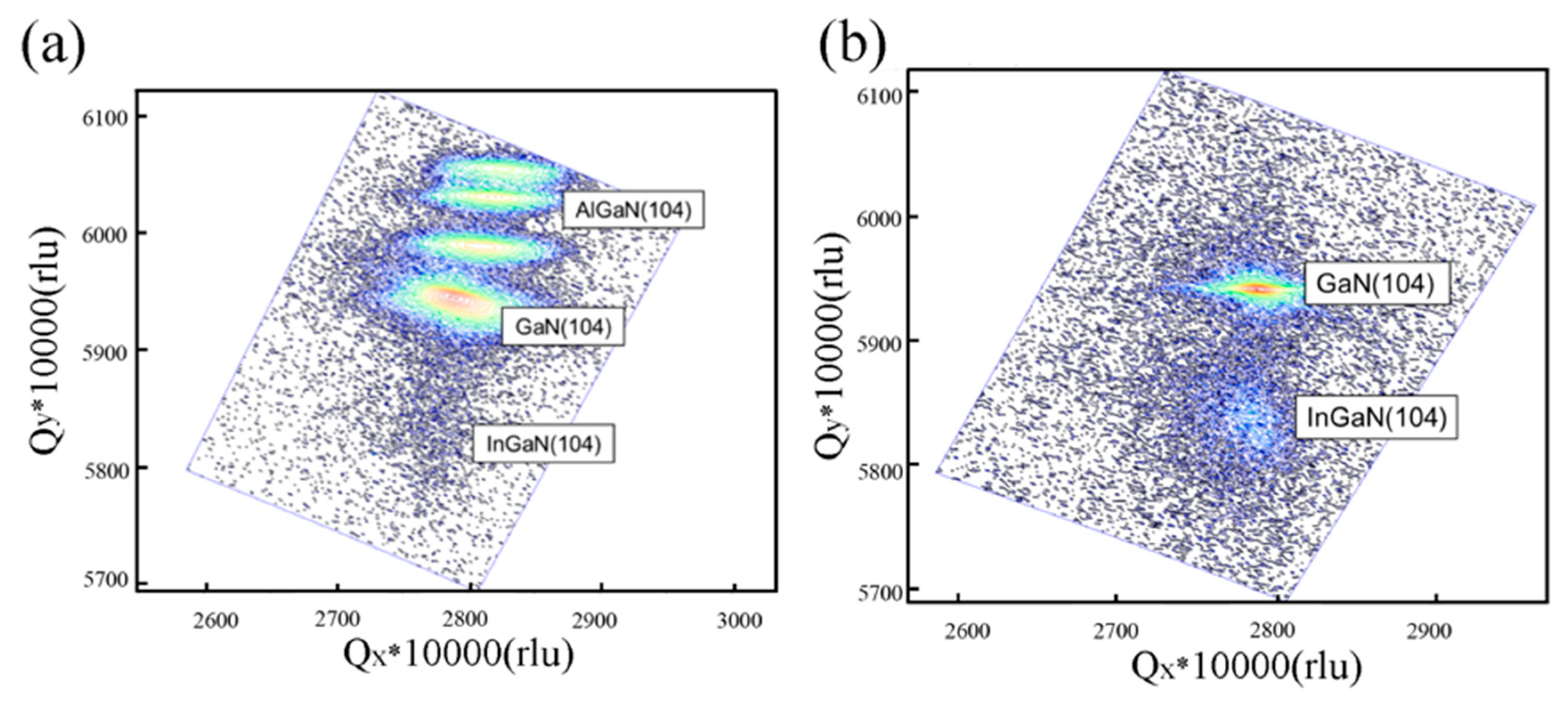
3. Results and Discussion

Figure 2a,b present the XRD 2theta-omega scan of the (002)-plane for the InGaN/GaN heterostructures grown at the temperature of 760 °C both on AlGaN/GaN-on-Si HEMT and GaN/sapphire template, respectively. Although the growth conditions are the same, the intensity of the InGaN peak for the (002) reflection on AlGaN/GaN-on-Si HEMT is much lower than that on GaN/sapphire template. This suggests a poor crystalline quality of the InGaN epilayer although the thickness is the same. The peak of the (002)-plane diffraction for the InGaN epilayer on the GaN/sapphire template is located at 33.93°, while this peak shifts to 33.98° when the InGaN is grown on the HEMT template. It should be noted that the peak of the GaN (002)-plane diffraction grown on sapphire is 34.56°, while it is 34.61° for that on the HEMT template. The different peak positions in the XRD diffraction are resulted from the different strain states in the GaN epilayers grown on different templates. Figure S1 in the supplementary material shows the XRD 2theta-omega scan of the GaN (002)-plane in the initial HEMT and sapphire substrate. It is found that, before InGaN deposition, the peak of the GaN (002)-plane is located at 34.56° on sapphire and changes to 34.61° on the HEMT template. Comparing to the standard peak of GaN (002)-plane diffraction which is located at 34.5692°, the strain in the GaN channel on the HEMT template is much higher than that in the GaN grown on sapphire substrate. The out-of-plane lattice constant c of the GaN channel in the HEMT structure is smaller (5.179 Å) than that on the sapphire substrate (5.186 Å), which indicates a tensile strain inside the in-plane direction. On the other hand, the (002)-plane diffraction peak of the GaN layer grown on the sapphire substrate is nearly the same as the standard one with little residual strain. The large strain in the GaN channel results in the different strain behaviors in the following InGaN layer. The crystalline quality of the GaN and InGaN layers on the two templates is further evaluated by the XRD rocking curves. The full-width-at-half-maximum (FWHM) values of the GaN on sapphire around (002)-plane is ~280 arcsec, while this value for GaN on the HEMT template is quite wide (1033 arcsec). The poor quality of the GaN channel on the HEMT template greatly influences the quality of the following InGaN epilayer. The (002)-planes of the InGaN on the AlGaN/GaN-on-Si HEMT and GaN/sapphire template are shown in Figure 2c,d, respectively. The FWHM values of the InGaN on the HEMT template and GaN/sapphire are 1590 and 1100 arcsec, respectively. The deteriorated crystalline quality of the InGaN on AlGaN/GaN-on-Si HEMT has originated from the poor-quality GaN channel with a high dislocation density.
As a result of the existence of the strain, the In composition cannot be simply calculated by the positions of XRD (002)-planes. The accurate estimation of the In composition, lattice constant, and relaxation degree is performed by analyzing the XRD reciprocal space mappings around the asymmetric diffraction planes. The relaxation degree is defined as: R (InGaN) = (aInGaNaGaN)/(a0InGaNa0GaN), where aInGaN and aGaN is the measured lattice parameters from RSMs, the a0InGaN is the relaxed parameters predicted by Vegard’s law, and the a0GaN is the relaxed GaN lattice constant [15]. Figure 3a,b are the RSMs of the two samples scanned around the (104)-plane for the InGaN/GaN on the AlGaN/GaN-on-Si HEMT and GaN/sapphire template, respectively. The results are listed in Table 1. From the calculation, the In composition considering strain in the InGaN on GaN/sapphire is 11% with an in-plane relaxation degree of 3.9% with regard to the GaN layer. On the other hand, for the InGaN/GaN heterostructure grown on the HEMT template, the In incorporation is increased to 16% and a higher relaxation degree approaching 30% is obtained. The higher In composition in the InGaN layer on the HEMT template is considered to have resulted from the compositional pulling effect by the higher relaxation degree. From the thermodynamic analysis, the compressive strain suppresses the In incorporation, whereas tensile strain promotes it [16]. The GaN channel in HEMT suffers from the tensile strain, leading to a relatively larger in-plane lattice constant aGaN. Therefore, the compressive strain between InGaN and GaN is reduced, resulting in a relatively higher In incorporation. On the other hand, the relaxation of epitaxial film by high-density dislocations also tends to induce a higher In incorporation.
The crystalline quality and the interface quality of the InGaN on HEMT templates can be improved by optimizing the growth conditions. The growth temperature of the InGaN is increased to 780 °C and the growth interruption during transition is controlled. The (002)-plane 2theta-omega scan by XRD of the heterostructure grown at 780 °C is displayed in Figure 4a. As can be seen, the diffraction intensity of the InGaN in the XRD has increased compared to that grown at 760 °C. The reflection fringes start to appear, indicating an abrupt interface morphology. The crystalline quality of the InGaN layer has greatly improved, as shown in Figure 4b of the rocking curve around the (002)-plane. The FWHM value is reduced to be 1260 arcsec. It should be pointed out that even grown on the poor-quality GaN channel (1033 arcsec), the quality of the InGaN is comparable to that grown on GaN/sapphire (280 arcsec for GaN/sapphire). Figure 5 is the XRD RSM of the InGaN/GaN around (104)-plane grown on the HEMT template at 780 °C. Table 1 summarizes the estimated lattice constant c of both GaN and InGaN, and relaxation degree from XRD reciprocal space mapping of the three samples. As can be seen, the In composition in the InGaN grown at 780 °C on the HEMT template is ~14%, slightly lower than that grown at 760 °C, but still higher than the In composition in the InGaN/GaN/sapphire grown at 760 °C. The relaxation degree of the InGaN layer is increased (73%). The reason for the higher relaxation degree is unclear. One possible reason may be the indium precipitation or the formation of three-dimensional islands when the temperature is higher. The PL spectra of the InGaN/GaN heterostructures grown on the HEMT template at different temperatures are shown in Figure S2. Compared to the luminescence of the InGaN/GaN on HEMT at 760 °C, the intensity of the InGaN/GaN at 780 °C is increased. The peak at ~365 nm is from the GaN near-band-edge (NBE) emission, and that at ~385 nm is corresponding to the NBE emission from the InGaN. The yellow band luminescence at ~550 nm is usually considered to be originated from the nitrogen vacancy-related defects in the structure. The ratio between the near-band-edge (NBE) and yellow band luminescence (YL) (INBE/IYL) can be a reflection for the quality of the epitaxial film. The INBE/IYL for the InGaN grown at 760 °C is 1.41, while it is enhanced with a ratio of 1.83 for the InGaN/GaN grown at 780 °C. This discloses an improved crystalline quality at elevated temperatures. The p-type conductivity in the InGaN/GaN heterojunctions are further confirmed by the Hall effect and Seebeck measurements.
From the above results, the growth and structure properties of InGaN/GaN heterostructures grown on the AlGaN/GaN-on-Si HEMT and GaN/sapphire templates are quite different. The poor-quality GaN in the HEMT structure results in a much wider FWHM value for the following InGaN epitaxial layer than that grown on GaN/sapphire template even deposited at the same conditions. Although the InGaN is nearly coherently grown on GaN/sapphire, it starts to be relaxed when grown on the AlGaN/GaN-on-Si HEMT at the same growth conditions. The In incorporation is also enhanced due to the relaxation of the epitaxial film. The quality and interface of the InGaN/GaN heterojunction can be improved by slightly increasing the growth temperature. However, the relaxation degree is increased, which becomes a problem for the InGaN/GaN heterostructure grown on the AlGaN/GaN-on-Si HEMT. Further optimization in the growth condition to control the strain is still needed.

4. Conclusions

In summary, the MOCVD growth and structure analysis of InGaN/GaN heterojunctions grown on AlGaN/GaN-on-Si HEMT templates are investigated and compared to the same structure grown on the GaN/sapphire template. It is found that the In composition and relaxation degree in the InGaN are quite different and dependent on the quality and strain state of the GaN bottom layers. The crystalline quality of the heterojunction on the AlGaN/GaN-on-Si HEMT is poor when the same growth condition is used due to the poor-quality GaN channel compared to that on the sapphire template. The In incorporation and relaxation degree are also higher. An increase of the growth temperature by 20 °C for the InGaN leads to an improved crystalline and interface quality. However, the relaxation degree is increased, which becomes a problem to maintain the high piezoelectric field. To achieve a high-performance p-channel transistor based on the InGaN/GaN heterojuntion on the AlGaN/GaN-on-Si HEMT, further studies on the structural optimization and growth optimization are still needed.

Supplementary Materials

The following are available online at https://www.mdpi.com/2076-3417/9/9/1746/s1.

Author Contributions

H.M. did the experiment and measurement. L.S. analyzed the experimental results and wrote down the paper. M.L. and B.R. helped on the discussion, paper revision and review. T.O., M.S., T.Y., and T.H. helped on the discussion, paper review and editing.

Acknowledgments

This work was supported by the JSPS KAKENHI Grant Number JP18K14141, World Premier International Research Center (WPI) initiative on Materials Nanoarchitectonics (MANA), Ministry of Education, Culture, Sports, Science & Technology (MEXT) in Japan.

Conflicts of Interest

The authors declare no conflict of interest.

References

  1. Ťapajna, M.; Hilt, O.; Bahat-Treidel, E.; Würfl, J.; Kuzmík, J. Investigation of gate-diode degradation in normally-off p-GaN/AlGaN/GaN high-electron-mobility transistors. Appl. Phys. Lett. 2015, 107, 193506. [Google Scholar] [CrossRef]
  2. Zhang, K.; Sumiya, M.; Liao, M.; Koide, Y.; Sang, L. P-channel InGaN/GaN heterostructure metal-oxide-semiconductor field effect transistor based on polarization induced two-dimensional hole gas. Sci. Rep. 2016, 6, 23683. [Google Scholar] [CrossRef] [PubMed]
  3. Zhou, H.; Lou, X.; Kim, S.B.; Chabak, K.D.; Gordon, R.G.; Peide, D.Y. Enhancement-Mode AlGaN/GaN Fin-MOSHEMTs on Si Substrate with Atomic Layer Epitaxy MgCaO. IEEE Electron. Device Lett. 2017, 38, 1294–1297. [Google Scholar] [CrossRef]
  4. Del Alamo, J.A. Nanometre-scale electronics with III-V compound semiconductors. Nature 2011, 479, 317. [Google Scholar] [CrossRef] [PubMed]
  5. Shatalov, M.; Simin, G.; Zhang, J.; Adivarahan, V.; Koudymov, A.; Pachipulusu, R.; Asif Khan, M. GaN-AlGaN p-channel inverted heterostructure JFET. IEEE Electron. Device Lett. 2002, 23, 452. [Google Scholar] [CrossRef]
  6. Li, G.; Wang, R.; Song, B.; Verma, J.; Cao, Y.; Ganguly, S.; Jena, D. Polarization-induced GaN-on-insulator E-D mode p-Channel heterostructure FETs. IEEE Electron. Device Lett. 2013, 34, 852. [Google Scholar] [CrossRef]
  7. Hahn, H.; Reuters, B.; Pooth, A.; Hollander, B.; Heuken, M.; Kalisch, H.; Vescan, A. p-channel enhancement and depletion mode GaN-based HFETs with quaternary backbarriers. IEEE Trans. Electron. Devices 2013, 60, 3005. [Google Scholar] [CrossRef]
  8. Hahn, H.; Reuters, B.; Pooth, A.; Noculak, A.; Kalisch, H.; Vescan, A. First small-signal data of GaN-based p-channel heterostructure field effect transistors. Jpn. J. Appl. Phys. 2013, 52, 128001. [Google Scholar] [CrossRef]
  9. Reuters, B.; Hahn, H.; Pooth, A.; Hollander, B.; Breuer, U.; Heuken, A.; Kalisch, H.; Vescan, A. Fabrication of p-channel heterostructure field effect transistors with polarization-induced two-dimensional hole gases at metal–polar GaN/AlInGaN interfaces. J. Phys. D Appl. Phys. 2014, 47, 175103. [Google Scholar] [CrossRef]
  10. Kumakura, K.; Makimoto, T.; Kobayashi, N. Mg-acceptor activation mechanism and transport characteristics in p-type InGaN grown by metalorganic vapor phase epitaxy. J. Appl. Phys. 2003, 93, 3370. [Google Scholar] [CrossRef]
  11. Yeo, Y.C.; Chong, T.C.; Li, M.F. Electronic band structures and effective-mass parameters of wurtzite GaN and InN. J. Appl. Phys. 1998, 83, 1429. [Google Scholar] [CrossRef]
  12. Yu, E.T.; Dang, X.Z.; Asbeck, P.M.; Lau, S.S.; Sullivan, G.J. Spontaneous and piezoelectric polarization effects in III-V nitride heterostructures. J. Vac. Sci. Technol. B 1999, 17, 1742. [Google Scholar] [CrossRef]
  13. Sang, L.; Liao, M.; Koide, Y.; Sumiya, M. High-performance metal-semiconductor-metal InGaN photodetectors using CaF2 as the insulator. Appl. Phys. Lett. 2011, 98, 103502. [Google Scholar] [CrossRef]
  14. Sang, L.; Liao, M.; Koide, Y.; Sumiya, M. InGaN-based thin film solar cells: Epitaxy, structural design and photovoltaic properties. J. Appl. Phys. 2015, 117, 105706. [Google Scholar] [CrossRef]
  15. Sang, L.W.; Qin, Z.X.; Fang, H.; Zhou, X.R.; Yang, Z.J.; Shen, B.; Zhang, G.Y. Study on threading dislocations blocking mechanism of GaN/AlxGa1−xN. Appl. Phys. Lett. 2008, 92, 192112. [Google Scholar] [CrossRef]
  16. Inatomi, Y.; Kangawa, Y.; Ito, T.; Suski, T.; Kumagai, Y.; Kakimoto, K.; Koukiku, A. Theoretical study of the composition pulling effect in InGaN metalorganic vapor-phase epitaxy growth. Jpn. J. Appl. Phys. 2017, 56, 078003. [Google Scholar] [CrossRef]
Figure 1. (a) Schematic diagram for the deposition process of the InGaN/GaN heterostructures, and (b) structure of the InGaN/GaN heterostructure on the AlGaN/GaN-on-Si high electron mobility transistor (HEMT) template.
Applsci 09 01746 g001
Figure 2. XRD 2theta-omega scan of the (002)-plane for the InGaN/GaN heterostructures at the growth temperature of 760 °C both on the (a) AlGaN/GaN-on-Si HEMT and (b) GaN/sapphire template. Corresponding XRD rocking curves of InGaN epitaxial layers on the (c) AlGaN/GaN-on-Si HEMT and (d) GaN/sapphire template, respectively.
Applsci 09 01746 g002
Figure 3. XRD reciprocal space mapping of (104)-plane for InGaN/GaN heterostructures at the temperature of 760 °C both on the (a) AlGaN/GaN-on-Si HEMT and (b) GaN/sapphire template.
Applsci 09 01746 g003
Figure 4. (a) XRD (002)-plane 2theta-omega scan for the InGaN/GaN heterostructure on AlGaN/GaN-on-Si HEMT at the temperature of 780 °C. (b) The corresponding XRD rocking curve of (002)-plane for the InGaN epitaxial layer.
Applsci 09 01746 g004
Figure 5. (a) XRD reciprocal space mapping of (104)-plane for the InGaN/GaN heterostructure grown on AlGaN/GaN-on-Si HEMT template at the temperature of 780 °C.
Applsci 09 01746 g005
Table 1. The out-of-plane lattice constant c of GaN, InGaN, and relaxation degree in InGaN layer of the three samples.
SampleCGaN (Å)CInGaN (Å)In%Relaxation (%)
InGaN/GaN on sapphire (760 °C)5.1865.280113.9
InGaN/GaN on HEMT (760 °C)5.1795.2721630
InGaN/GaN on HEMT (780 °C)5.1805.2691473

