Tunable Silver Nanoparticle Arrays by Hot Embossing and Sputter Deposition for Surface-Enhanced Raman Scattering


Abstract
Featured Application
Abstract
1. Introduction
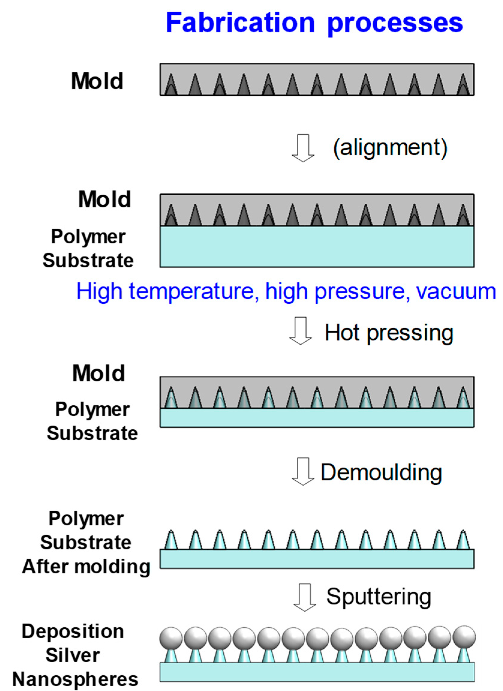
2. Methodology
3. Experiments
4. Results and Discussion
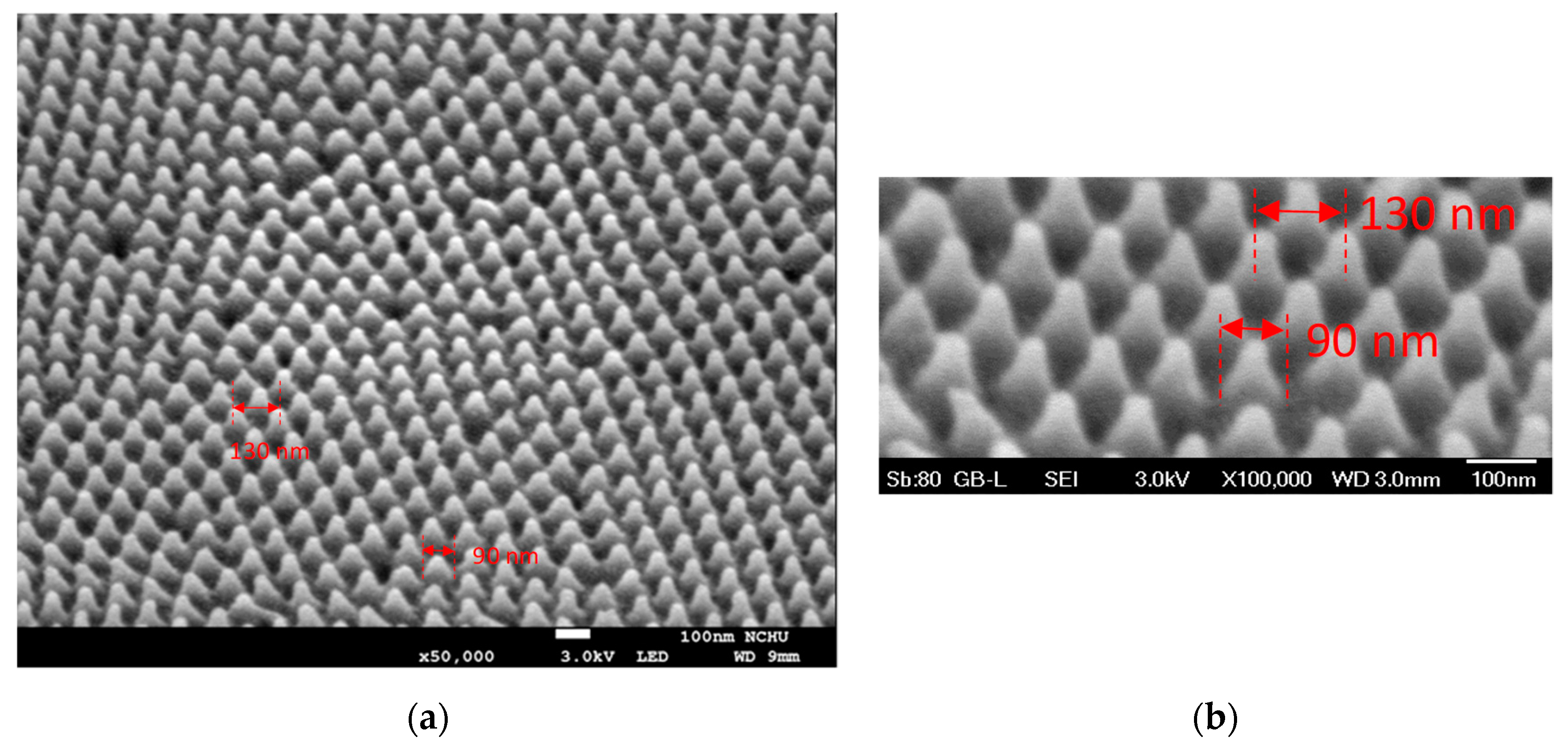
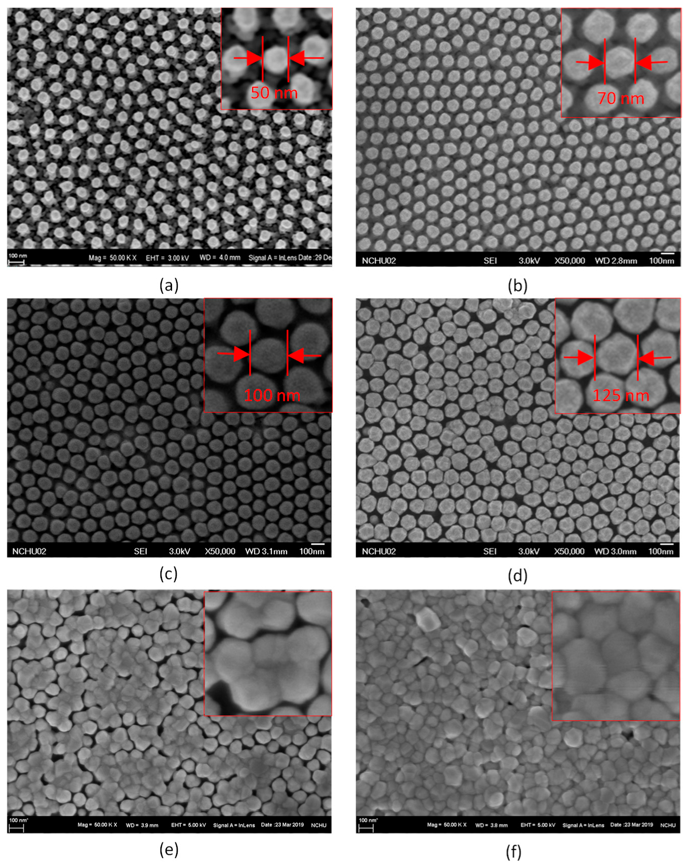
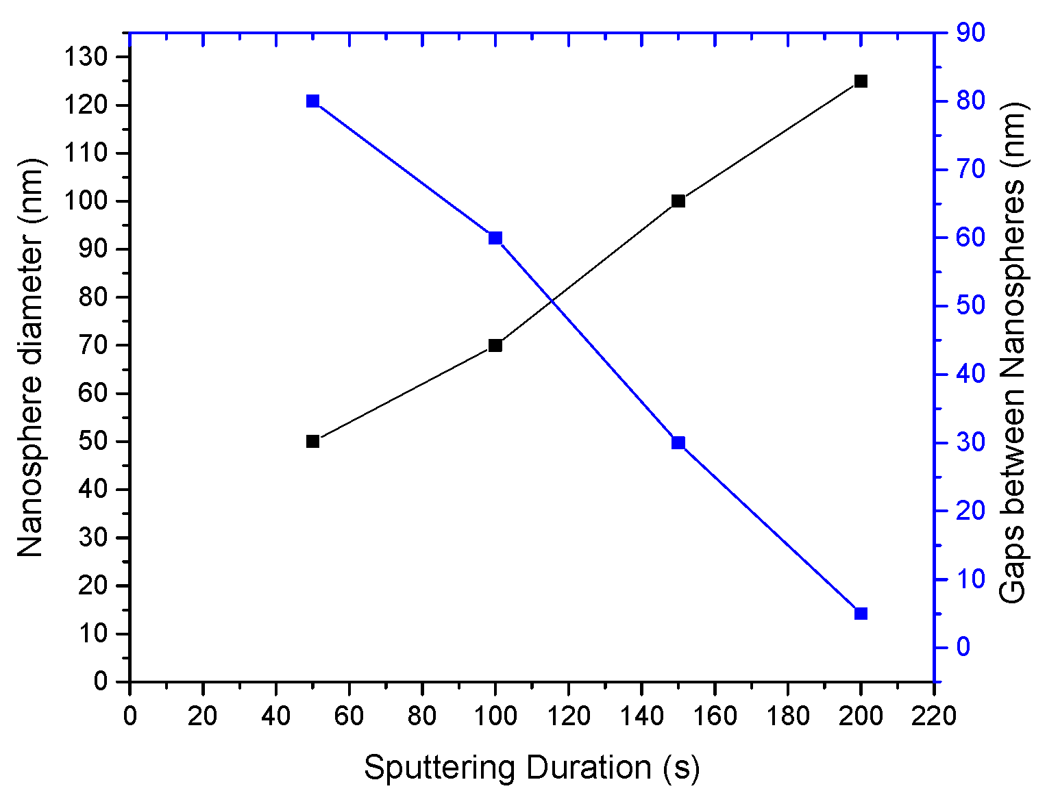
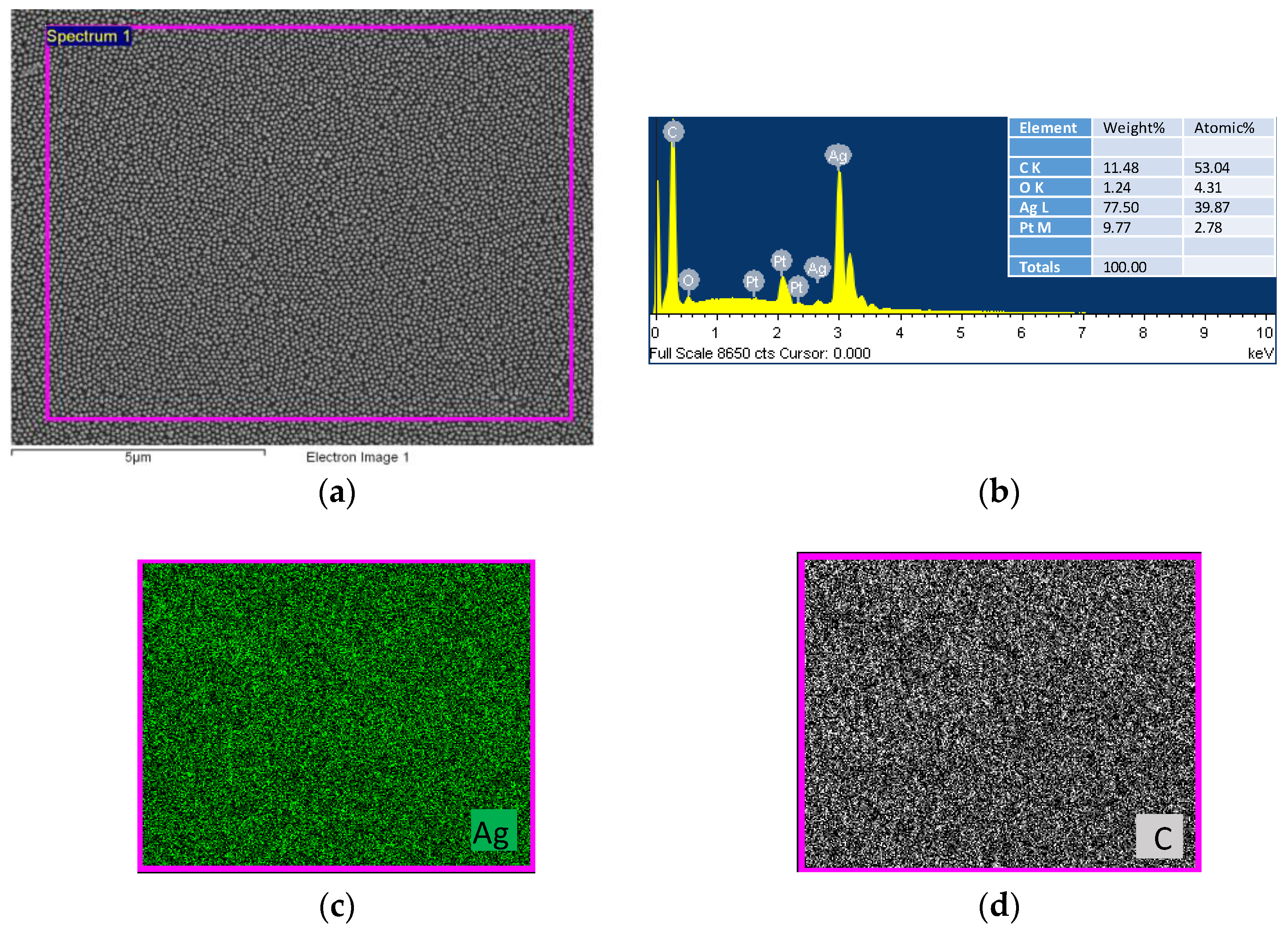
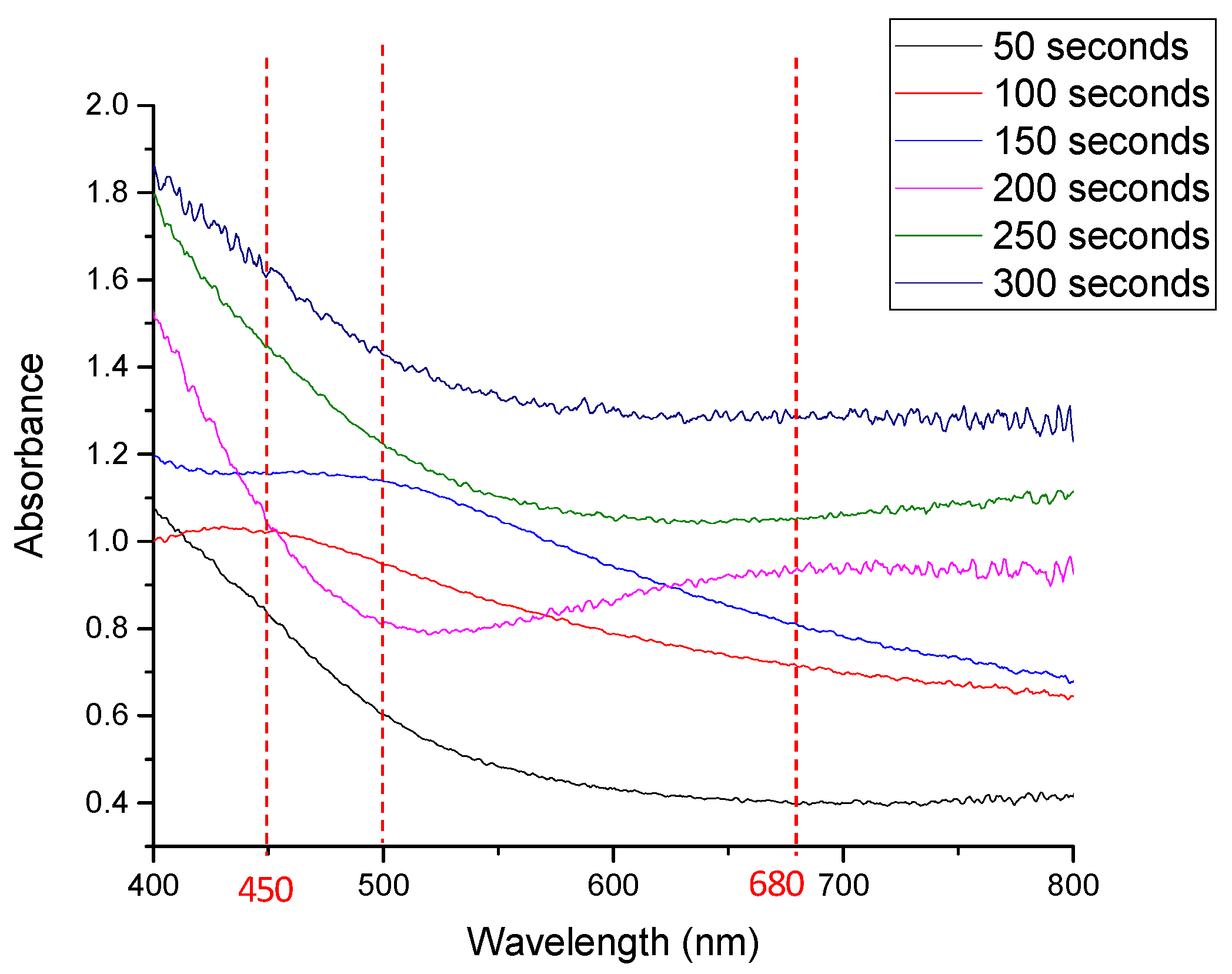
4.1. Characterization of the Developed Substrates
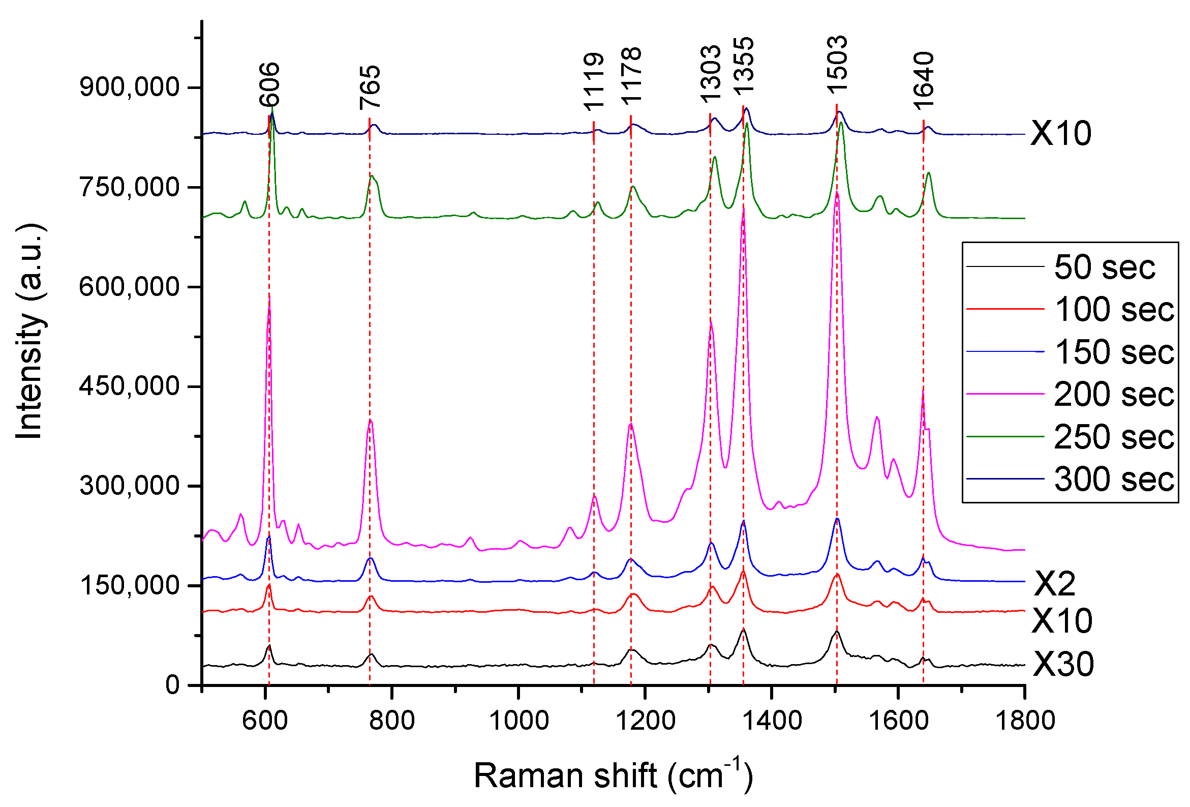
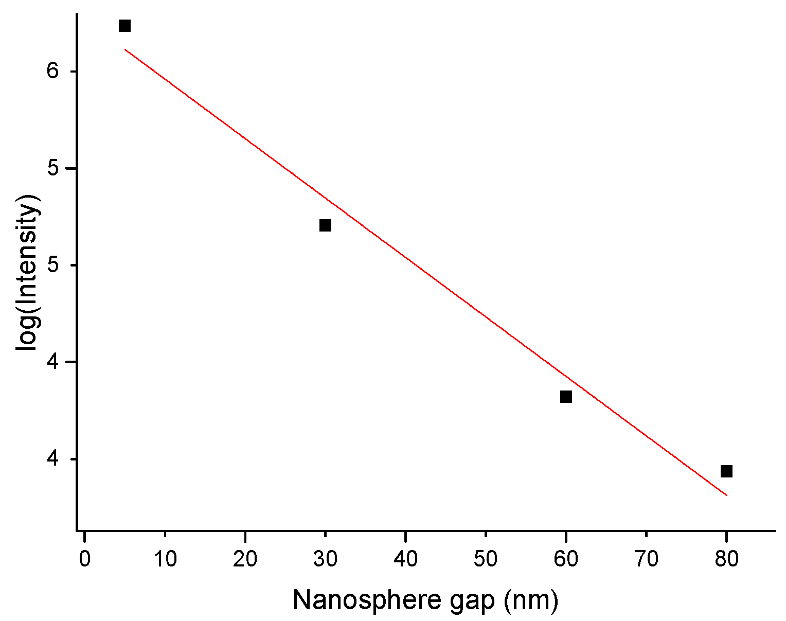
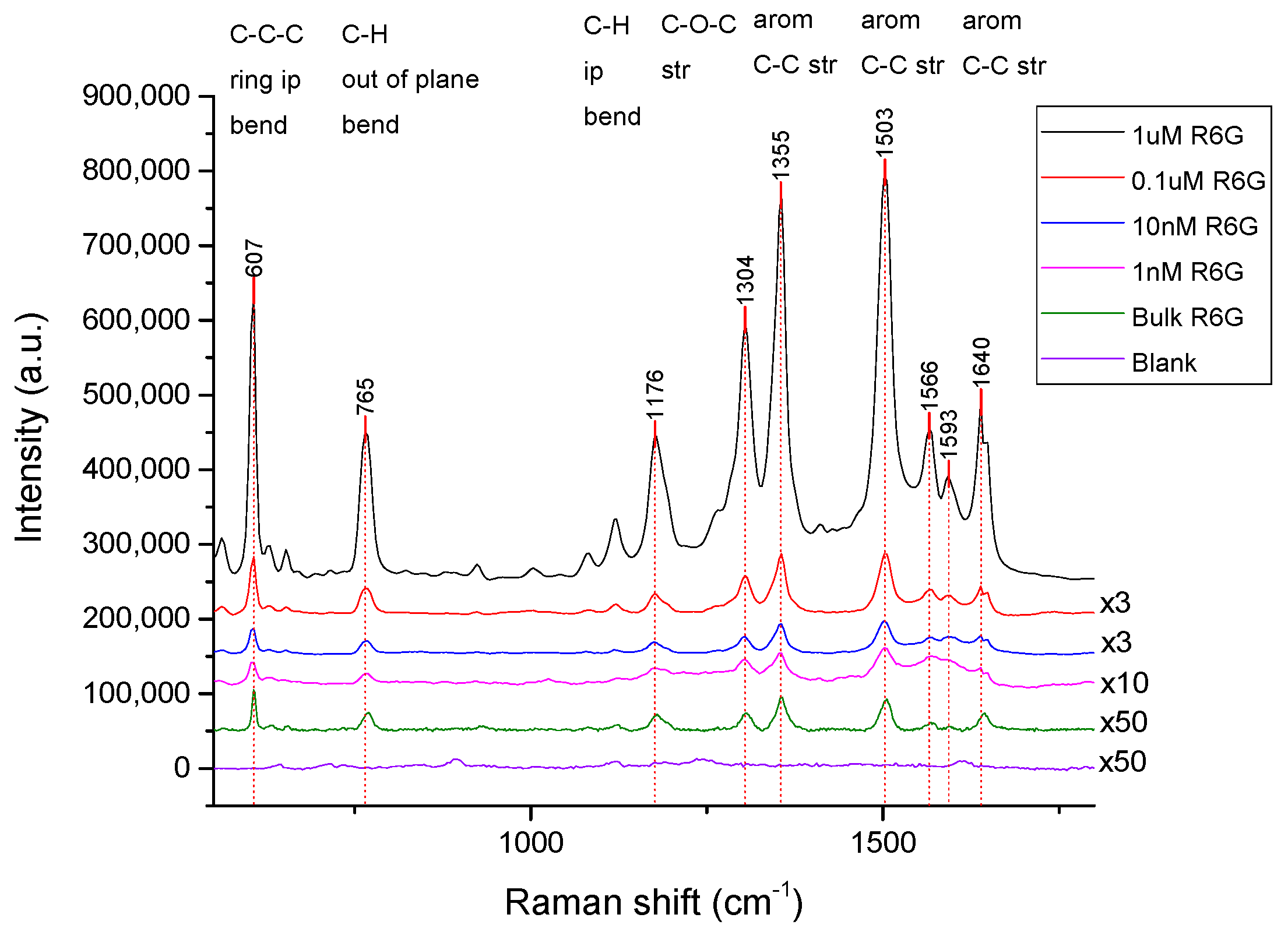
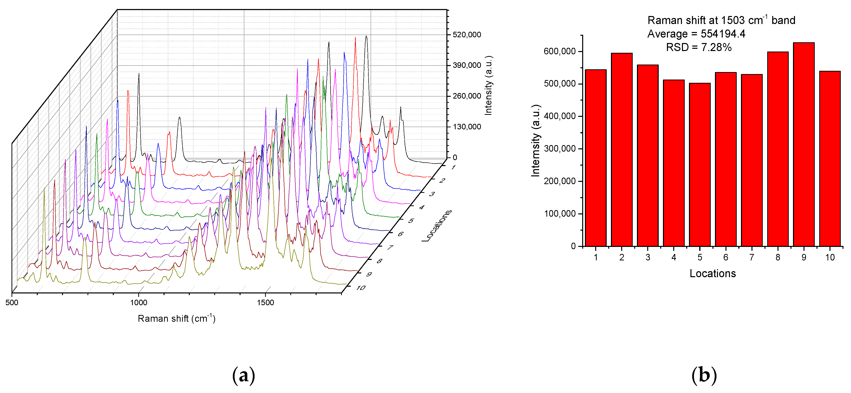
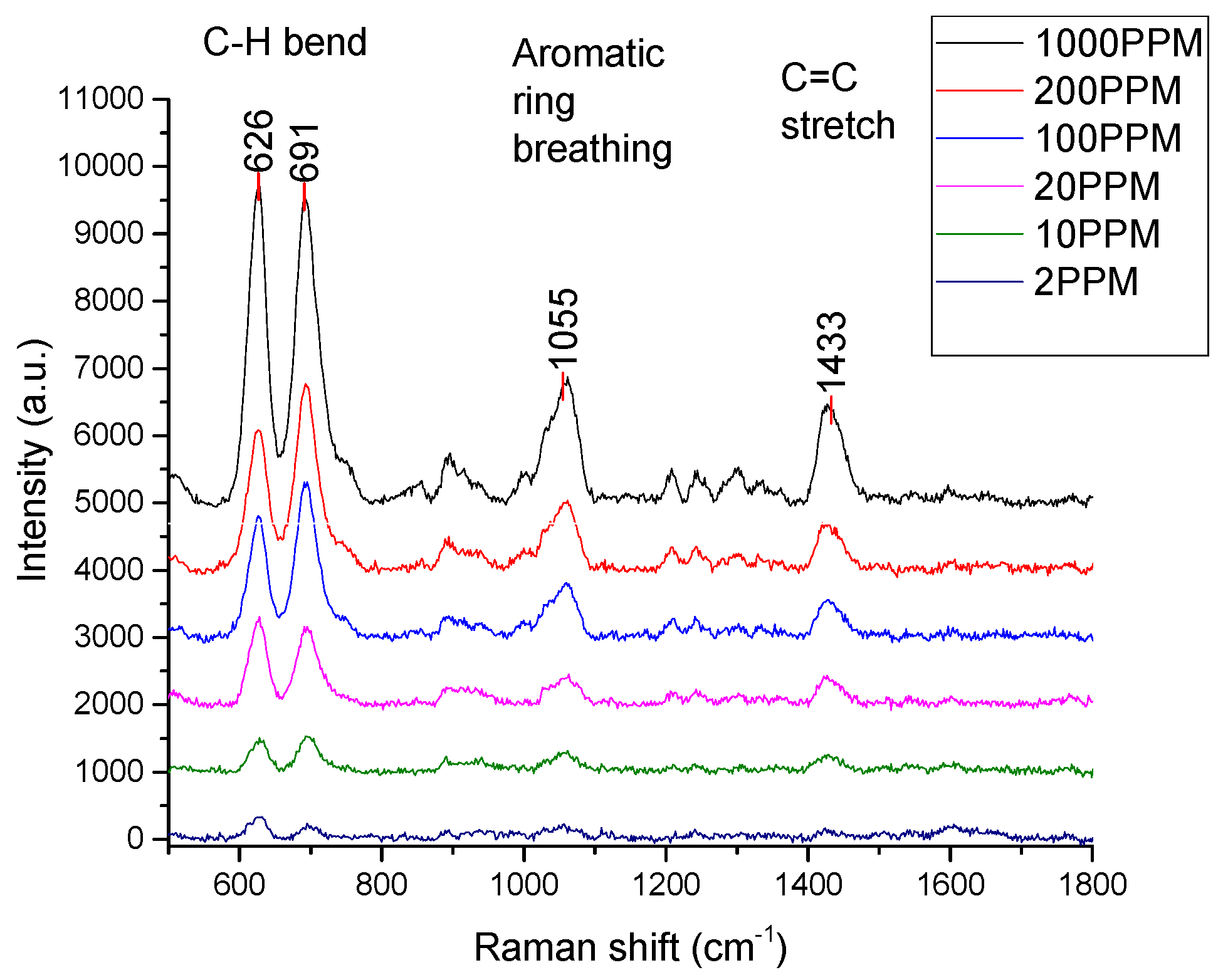
4.2. Performance of the SERS Substrates
5. Conclusions
Author Contributions
Funding
Acknowledgments
Conflicts of Interest
References
- Fleischmann, M.; Hendra, P.J.; McQuillan, A.J. Raman spectra of pyridine adsorbed at a silver electrode. Chem. Phys. Lett. 1974, 26, 163–166. [Google Scholar] [CrossRef]
- Le Ru, E.C.; Blackie, E.; Meyer, M.; Etchegoin, P.G. Surface enhanced raman scattering enhancement factors: A comprehensive study. J. Phys. Chem. 2007, 111, 13794–13803. [Google Scholar] [CrossRef]
- Bantz, K.C.; Meyer, A.F.; Wittenberg, N.J.; Im, H.; Kurtuluş, Ö.; Lee, S.H.; Lindquist, N.C.; Oh, S.H.; Haynes, C.L. Recent progress in SERS biosensing. Phys. Chem. Chem. Phys. 2011, 13, 11551–11567. [Google Scholar] [CrossRef] [PubMed]
- Alvarez-Puebla, R.A.; Liz-Marzán, L.M. SERS-Based diagnosis and biodetection. Small 2010, 6, 604–610. [Google Scholar] [CrossRef] [PubMed]
- Caro, C.; Quaresma, P.; Pereira, E.; Franco, J.; Pernia Leal, M.; García-Martín, M.L.; Royo, J.L.; Oliva-Montero, J.M.; Merkling, P.J.; Zaderenko, A.P.; et al. Synthesis and characterization of elongated-shaped silver nanoparticles as a biocompatible anisotropic SERS probe for intracellular imaging: Theoretical modeling and experimental verification. Nanomaterials 2019, 9, 256. [Google Scholar] [CrossRef] [PubMed]
- Cañamares, M.V.; Sevilla, P.; Sanchez-Cortes, S.; Garcia-Ramos, A.V. Surface-enhanced Raman scattering study of the interaction of red dye alizarin with ovalbumin. Biopolym. Orig. Res. Biomol. 2006, 82, 405–409. [Google Scholar] [CrossRef]
- An, Q.; Zhang, P.; Li, J.M.; Ma, W.F.; Guo, J.; Hu, J.; Wang, C.C. Silver-coated magnetite–carbon core–shell microspheres as substrate-enhanced SERS probes for detection of trace persistent organic pollutants. Nanoscale 2012, 4, 5210–5216. [Google Scholar] [CrossRef] [PubMed]
- Cao, Q.; Che, R. Tailoring Au–Ag–S Composite Microstructures in One-Pot for Both SERS Detection and Photocatalytic Degradation of Plasticizers DEHA and DEHP. ACS Appl. Mater. Interfaces 2014, 6, 7020–7027. [Google Scholar] [CrossRef] [PubMed]
- Liu, Z.; Yang, Z.; Peng, B.; Cao, C.; Zhang, C.; You, H.; Xiong, Q.; Li, Z.; Fang, J. Highly Sensitive, Uniform, and Reproducible Surface-Enhanced Raman Spectroscopy from Hollow Au-Ag Alloy Nanourchins. Adv. Mater. 2014, 26, 2431–2439. [Google Scholar] [CrossRef]
- Anderson, D.J.; Moskovits, M. A SERS-Active System Based on Silver Nanoparticles Tethered to a Deposited Silver Film. J. Phys. Chem. B 2006, 110, 13722–13727. [Google Scholar] [CrossRef]
- Cialla, D.; März, A.; Böhme, R.; Theil, F.; Weber, K.; Schmitt, M.; Popp, J. Surface-enhanced Raman spectroscopy (SERS): Progress and trends. Anal. Bioanal. Chem. 2012, 403, 27–54. [Google Scholar] [CrossRef] [PubMed]
- Love, S.A.; Marquis, B.J.; Haynes, C.L. Recent advances in nanomaterial plasmonics: Fundamental studies. Appl. Spectrosc. 2008, 62, 346A–362A. [Google Scholar] [CrossRef]
- Mu, C.; Zhang, J.P.; Xu, D. Au nanoparticle arrays with tunable particle gaps by template-assisted electroless deposition for high performance surface-enhanced Raman scattering. Nanotechnology 2010, 21, 015604. [Google Scholar] [CrossRef] [PubMed]
- Lee, S.J.; Guan, Z.; Xu, H.; Moskovits, M. Surface-Enhanced Raman Spectroscopy and Nanogeometry: The Plasmonic Origin of SERS. J. Phys. Chem. 2007, 111, 17985–17988. [Google Scholar] [CrossRef]
- Sánchez-Iglesias, A.; Aldeanueva-Potel, P.; Ni, W.; Pérez-Juste, J.; Pastoriza-Santos, I.; Alvarez-Puebla, R.A.; Mbenkum, B.N.; Liz-Marzán, L.M. Chemical seeded growth of Ag nanoparticle arrays and their application as reproducible SERS substrates. Nano Today 2010, 5, 21–27. [Google Scholar] [CrossRef]
- Nuntawong, N.; Eiamchai, P.; Wong-ek, B.; Horprathum, M.; Limwichean, K.; Patthanasettakul, V.; Chindaudom, P. Shelf time effect on SERS effectiveness of silver nanorod prepared by OAD technique. Vacuum 2013, 88, 23–27. [Google Scholar] [CrossRef]
- Singh, J.P.; Chu, H.; Abell, J.; Tripp, R.A.; Zhao, Y. Flexible and mechanical strain resistant large area SERS active substrates. Nanoscale 2012, 4, 3410–3414. [Google Scholar] [CrossRef] [PubMed]
- Runge, J.M. The Metallurgy of Anodizing Aluminum; Springer International Publishing: Cham, Switzerland, 2018. [Google Scholar]
- Brzózka, A.; Szeliga, D.; Kurowska-Tabor, E.; Sulka, G.D. Synthesis of copper nanocone array electrodes and its electrocatalytic properties toward hydrogen peroxide reduction. Mater. Lett. 2016, 174, 66–70. [Google Scholar] [CrossRef]
- Huang, C.Y.; Tsai, M.S. Fabrication of 3D nano-hemispherical cavity array plasmonic substrate for SERS applications. Int. J. Optomechatron. 2018, 12, 40–52. [Google Scholar] [CrossRef]
- Geissler, M.; Li, K.; Cui, B.; Clime, L.; Veres, T. Plastic Substrates for Surface-Enhanced Raman Scattering. J. Phys. Chem. C 2009, 113, 17296–17300. [Google Scholar] [CrossRef]
- Freeman, R.G.; Grabar, K.C.; Allison, K.J.; Bright, R.M.; Davis, J.A.; Guthrie, A.P.; Hommer, M.B.; Jackson, M.A.; Smith, P.C.; Walter, D.G.; et al. Self-Assembled Metal Colloid Monolayers: An Approach to SERS Substrates. Science 1995, 267, 1629–1632. [Google Scholar] [CrossRef] [PubMed]
- Araújo, A.; Caro, C.; Mendes, M.J.; Nunes, D.; Fortunato, E.; Franco, R.; Águas, H.; Martins, R. Highly efficient nanoplasmonic SERS on cardboard packaging substrates. Nanotechnology 2014, 25, 415202. [Google Scholar] [CrossRef] [PubMed]
- Araújo, A.; Pimentel, A.; Oliveira, M.J.; Mendes, M.J.; Franco, R.; Fortunato, E.; Águas, H.; Martins, R. Direct growth of plasmonic nanorod forests on paper substrates for low-cost flexible 3D SERS platforms. Flex. Print. Electron. 2017, 2, 014001. [Google Scholar] [CrossRef]
- Caro, C.; Gámez, F.; Zaderenko, A.P. Preparation of Surface-Enhanced Raman Scattering Substrates Based on Immobilized Silver-Capped Nanoparticles. J. Spectrosc. 2018, 2018, 1–9. [Google Scholar] [CrossRef]
- Wu, W.; Liu, L.; Dai, Z.; Liu, J.; Yang, S.; Zhou, L.; Xiao, X.; Jiang, C.; Roy, V.A. Low-Cost, Disposable, Flexible and Highly Reproducible Screen Printed SERS Substrates for the Detection of Various Chemicals. Sci. Rep. 2015, 5, 10208. [Google Scholar] [CrossRef] [PubMed]
- Sree Satya Bharati, M.; Byram, C.; Soma, V.R. Femtosecond Laser Fabricated Ag@Au and Cu@Au Alloy Nanoparticles for Surface Enhanced Raman Spectroscopy Based Trace Explosives Detection. Front. Phys. 2018, 6, 28. [Google Scholar] [CrossRef]


© 2019 by the authors. Licensee MDPI, Basel, Switzerland. This article is an open access article distributed under the terms and conditions of the Creative Commons Attribution (CC BY) license (http://creativecommons.org/licenses/by/4.0/).
Share and Cite
Huang, C.-Y.; Tsai, M.-S. Tunable Silver Nanoparticle Arrays by Hot Embossing and Sputter Deposition for Surface-Enhanced Raman Scattering. Appl. Sci. 2019, 9, 1636. https://doi.org/10.3390/app9081636
Huang C-Y, Tsai M-S. Tunable Silver Nanoparticle Arrays by Hot Embossing and Sputter Deposition for Surface-Enhanced Raman Scattering. Applied Sciences. 2019; 9(8):1636. https://doi.org/10.3390/app9081636
Chicago/Turabian StyleHuang, Chu-Yu, and Ming-Shiuan Tsai. 2019. "Tunable Silver Nanoparticle Arrays by Hot Embossing and Sputter Deposition for Surface-Enhanced Raman Scattering" Applied Sciences 9, no. 8: 1636. https://doi.org/10.3390/app9081636
APA StyleHuang, C.-Y., & Tsai, M.-S. (2019). Tunable Silver Nanoparticle Arrays by Hot Embossing and Sputter Deposition for Surface-Enhanced Raman Scattering. Applied Sciences, 9(8), 1636. https://doi.org/10.3390/app9081636