Featured Application
Power supply construction for dielectric barrier or corona discharge, atmospheric pressure plasma reactors.
Abstract
Non-thermal plasma reactors offer numerous advantages and are used in a wide variety of applications. Exemplary fields of use include exhaust gas or water quality improvement, surface processing, agriculture, or medical processes. Two of the most popular discharge chamber constructions are dielectric barrier discharge (DBD) and pulsed corona discharge (PCD, barrierless) plasma reactors. Various power supply constructions are presented in the literature with varying complexity and operating principles. A simple, power electronic, pulsed power supply construction is presented in this work, implementing resonant power switch operation, modern silicon carbide (SiC) power semiconductors and a Tesla coil-like transformer design. The power supply construction is immune to short circuits in the reactor and can be used for both types of reactor constructions. The principles of operation, simulation results, and prototype test verifications are presented with main power supply characteristics.
1. Introduction
Non-thermal plasma discharge properties are used in a wide variety of processes. The main applications include agricultural use [1], medical processing [2], water and exhaust treatment [3,4], waste air quality improvement, and deodorization [5,6,7]. Further research is needed to provide application possibilities in different fields [4]. Regarding the plasma reactor constructions, dielectric barrier discharge (DBD, electrodes separated by a dielectric barrier) and corona discharge (CD, separated electrodes with no dielectric barrier) reactors are most widely used for cold plasma discharge generation under atmospheric pressure. The different properties of both constructions are an important factor in choosing a certain one for industrial applications and have a strong influence on power supply system designs.
In order to efficiently supply a plasma module, many different power supply topologies and electrical waveforms exist. It is possible to use a simple, high-voltage sine wave source (from several to several tens of kV) with a frequency of 50 Hz to 50 kHz to generate the plasma in a DBD reactor. To generate plasma in CD reactors, it is necessary to have a high-voltage pulsed source (from several to several tens of kV), with a high-voltage steepness (typically in the range from several hundred to several thousand volts/ns [8]. Since the construction of CD reactors is much simpler and they have a smaller flow resistance than a typical DBD reactor, a highly efficient topology is required for a High Voltage (HV) generator. Additionally, when using a HV pulse generator for DBD reactors, it is also possible to significantly improve the energy efficiency of plasma generation [9]. Currently, in the generation of high-voltage pulse systems of rotating gas gaps, gas gaps with trigger electrodes or thyratrons as well as fast ionizing dynistors (FIDs) are often used. From the viewpoint of the dynamic parameters of modern power transistors (such as SiC or GaN MOSFETs), the implementation of HV pulse generators is possible.
This paper is organized as follows: In the first section, the description of proposed high-voltage resonant converter with simulation results is provided, followed by the design and construction details, and suggestions are discussed for a prototype power supply. Finally, measurement results of the experimental setup and practical verification of properties with different types of loads are presented.
2. Materials and Methods
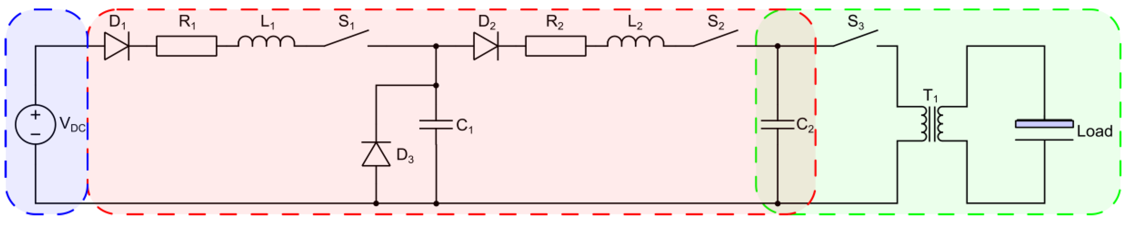
A new, simple topology of the pulsed power supply is depicted in Figure 1. It consists of three main conversion stages: (a) a DC voltage source; (b) a resonant charger circuit constituting the initial pulse energy by the voltage control of the capacitor C2; and (c) an output pulse shaper with Tesla coil-like transformer. In order to investigate the basic operation, role, and properties of each stage, they will be discussed separately, in detail, in the following subsections.
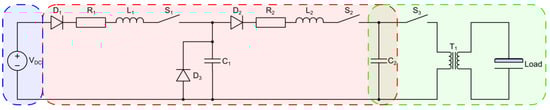
Figure 1.
Proposed pulsed power supply for non-thermal plasma reactors. Three main stages are marked: DC voltage source (blue); resonant capacitor charger (red); and output pulse shaping unit (green).
2.1. The DC Voltage Source
The first part of the proposed high-voltage power supply is a DC voltage source whose output voltage value may be fixed at several hundreds of volts (using a passive rectifier circuit or an active PFC stage), or variable up to similar values (300–650 V is the most useful and commonly used range [10]). In a specific application, this topology can be fed directly from the mains with a simple rectifier circuit with capacitor bank. In other cases—especially when galvanic isolation from the power grid is required—an isolated AC/DC power supply should be used.
In order to verify the laboratory prototype properties for different input voltage values, the laboratory TDK Lambda GEN600-2.6 SMPS (switching mode power supply) voltage source was used. This provided stable voltage with a control range from 0 to 650 V DC, and 2.6 A of average output current. The high efficiency and galvanic isolation of the used power supply were additional advantageous features.
2.2. The Resonant Capacitor Charger
The presented power supply should generate high-voltage pulses with adjustable amplitude and repetition ratio. The repetition frequency of the output voltage pulses was set in the range of 250–2000 Hz. The role of the resonant capacitor charger is to accumulate the energy needed to generate a single voltage pulse in the electric field of a capacitor bank. The charging process must have acceptable accuracy and has to be fast enough to finish in the available time (pause) between output pulses. A simple, resonant construction with two power switches was chosen to reduce the switching loss of the used power semiconductors, and to make the charging process as efficient as possible.
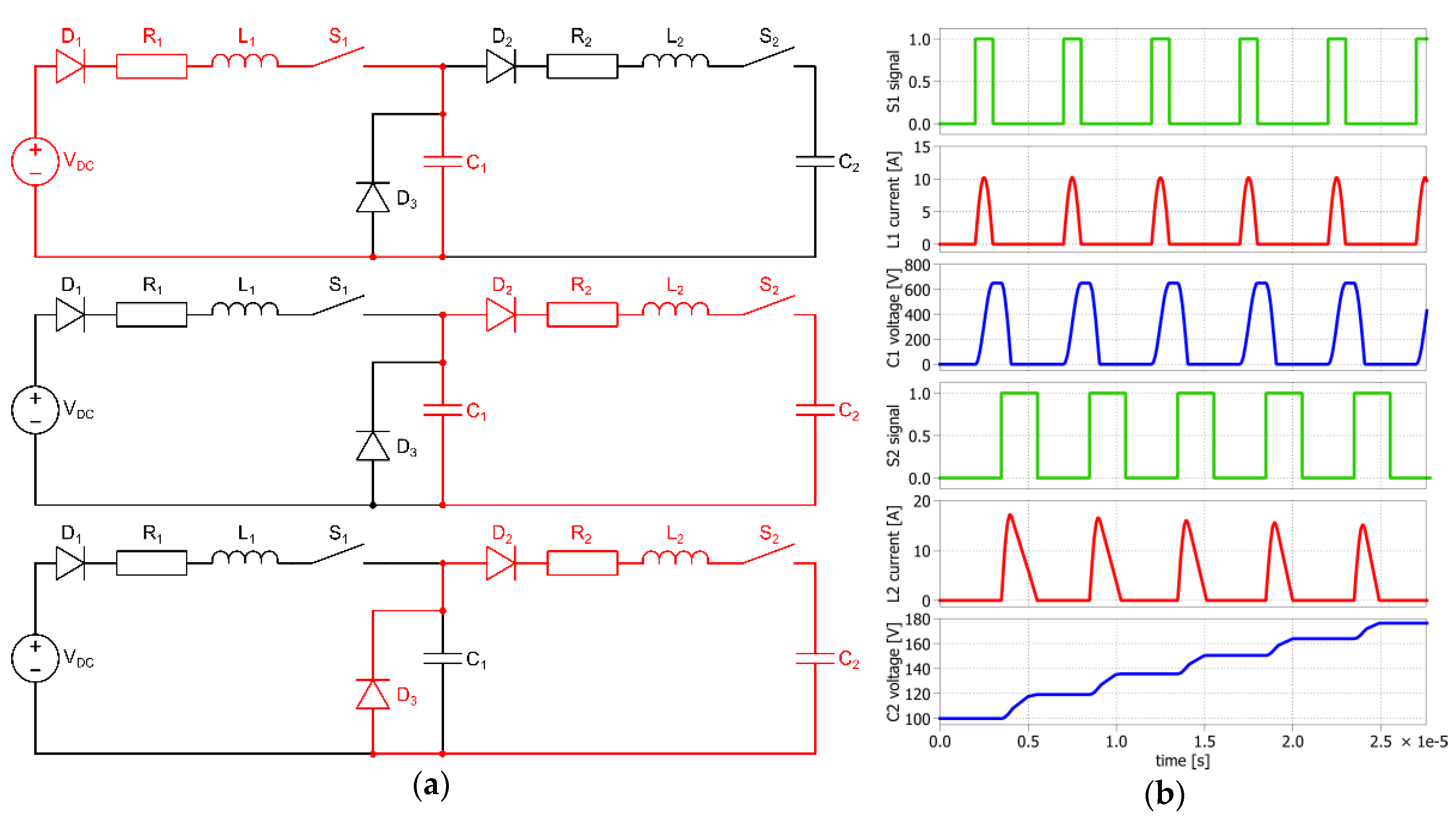
The proposed topology acts in three repetitive intervals, as shown in Figure 2. The analytical description of this part of the topology and each separate interval were presented in [11].
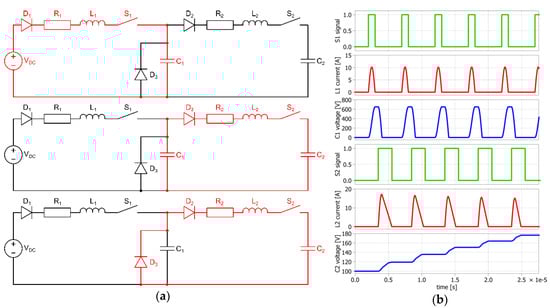
Figure 2.
(a) The three intervals of capacitor charger operation and (b) simulated waveforms. PLECS® simulation platform was used for calculations. Interval 1 (top)—the energy of the input source is resonantly transferred to capacitor (with voltage boost effect) C1. Interval 2 (middle)—the energy of capacitor C1 is resonantly transferred to C2 and increases the voltage across C2. Interval 3 (bottom)—the resonant energy stored in the magnetic field of L2 is used to charge C2 using the freewheeling diode D3.
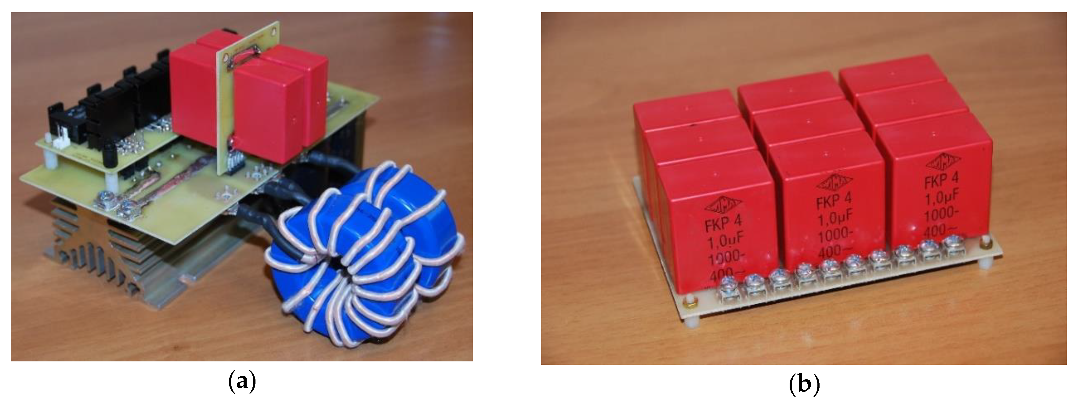
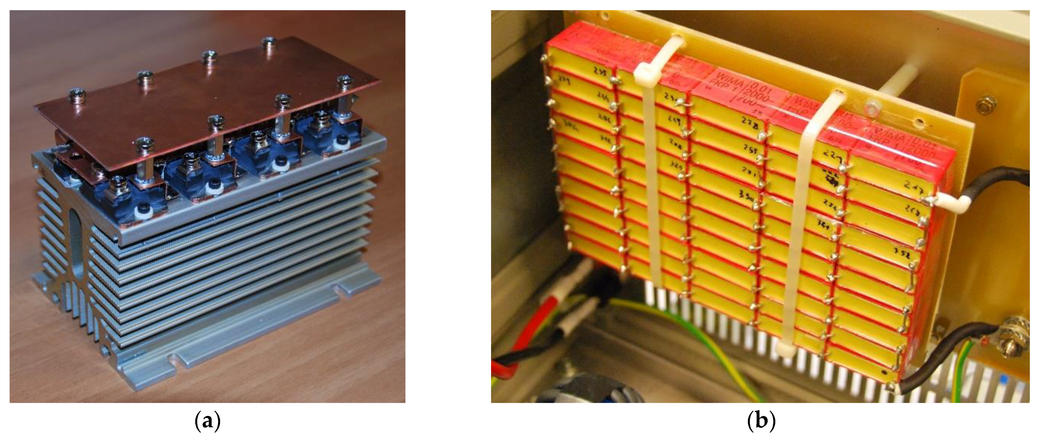
The proposed resonant charger consists of two series of monoresonant RLC (resistive – inductive – capacitive) circuits connected in a cascade. In the real power supply construction, inductors L1 and L2 were made of single MS-250026-2 micrometals cores with 15 turns each using litz wire windings of ~5.8 mm2 of copper wire to obtain an inductance of 22 uH. R1 and R2 are the parasitic resistances of inductors, wires, and printed circuit board tracks, in the real construction, the measured value was 17 mΩ. The core material used is called SENDUST, and it is designed for high-frequency power application inductors. The C1 capacitance has a measured value of 12 nF in the prototype and is made of WIMA FKP capacitors connected in series, due to the high dV/dt operation of that power supply stage. The C2 capacitance is a 1 uF capacitor bank made of nine 1 uF WIMA FKP capacitors connected in a mixed (parallel series) way, due to the high value of the capacitor current. Figure 3 shows the constructed resonant capacitor charger module and the C2 capacitor bank.
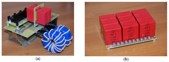
Figure 3.
(a) The resonant capacitor charger and (b) the C2 capacitor bank.
For those values of the real L and C components, the charging of C1 capacitance takes 1.5 µs and the energy transfer between C1 and C2 takes 1.5 µs. To fully charge the C2 capacitor, 30 repetitions of three charging intervals are needed. The power switches S1 and S2 were 1700 V, 72 A, 45 mΩ SiC power MOSFETs C2M0045170D from Cree. The diodes D1–D3 were 1700 V, 10 A SiC power Schottky diodes GB10MPS17 from GeneSiC Semiconductor Inc. The diodes D1 and D2 prevent the reverse flow of energy and, therefore, a low reverse recovery current feature of SiC diodes could be used. The role of the diode D3 is to block the negative current flow of the resonating tank to exclude negative voltages on the capacitor C1.
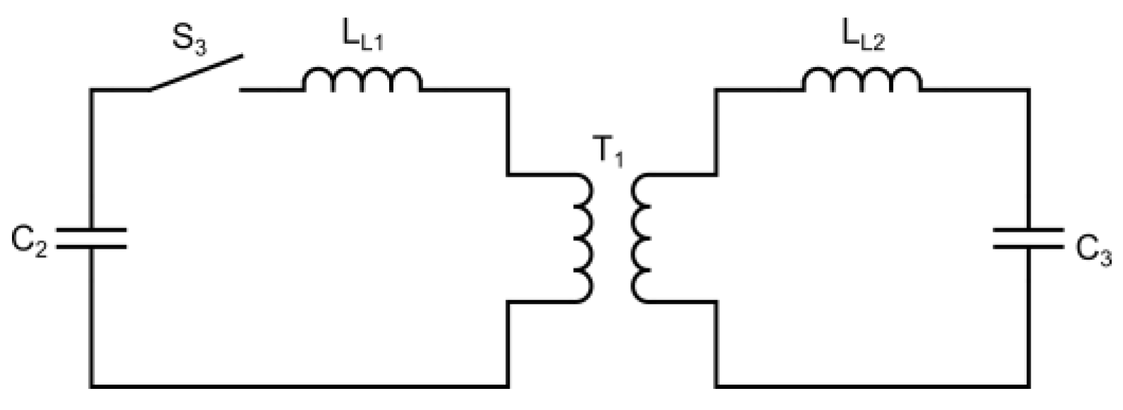
2.3. The Output Pulse Shaping Unit
The most important part of the presented high-voltage pulsed converter design is the output stage based on the Tesla transformer concept. This allows for shaping of the output voltage pulse through the resonance of the circuit’s L and C components, as schematically depicted in Figure 4. To obtain the highest amplitudes of output voltage pulse without mutual oscillations between pulses, the magnetic coupling coefficient k should be equal to approx. 0.6, and the rules of Equation (1) must be fulfilled [12,13].
LL1∙C2 = LL2∙C3 (ω1 = ω2)

Figure 4.
Output pulse shaping circuit with Tesla coil-like cored transformer.
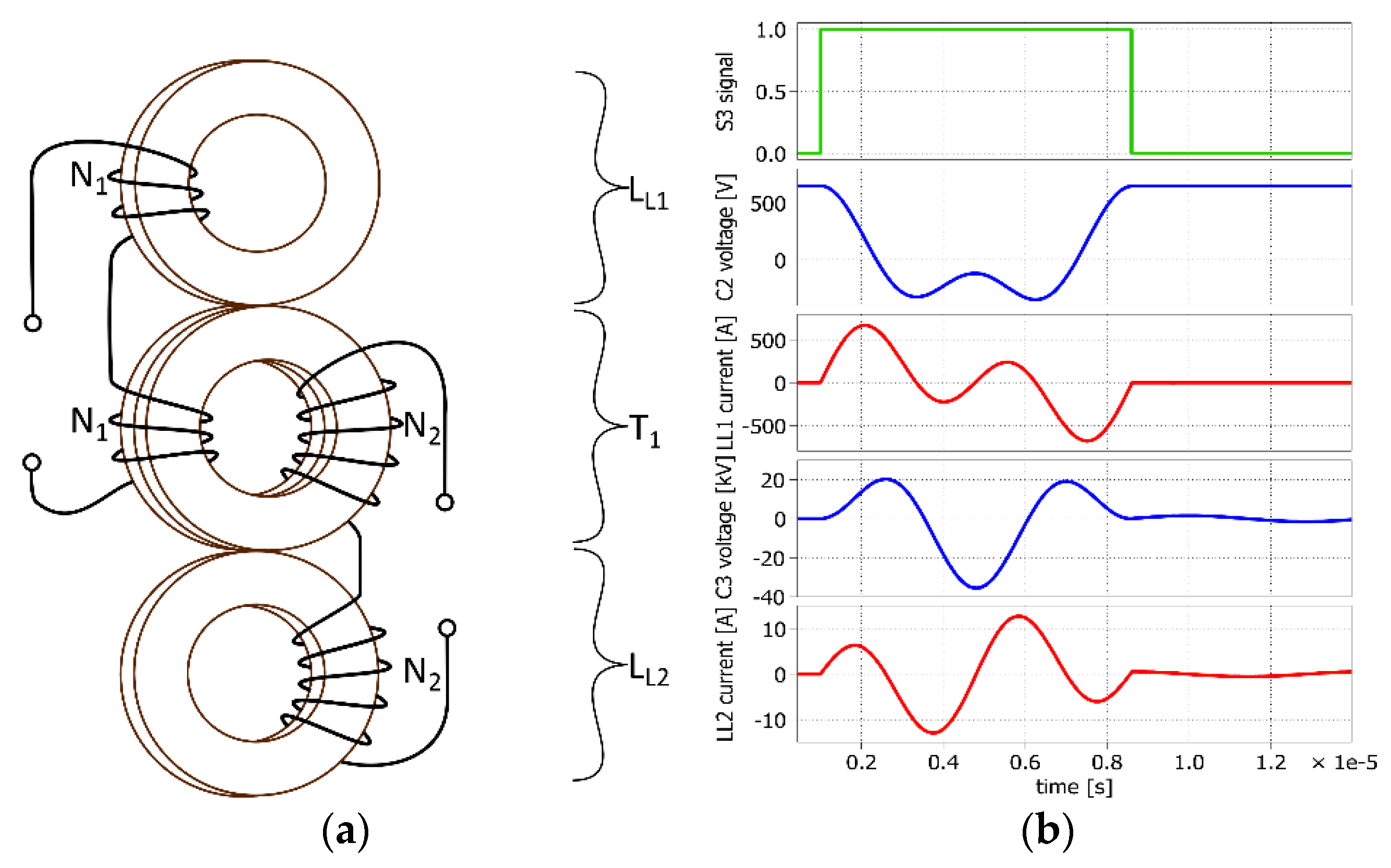
Most Tesla-based transformers are coreless (air coupling) but there are also constructions with magnetic cores [14]. Low permeability magnetic cores (e.g., distributed gap cores) were used in the presented design, instead of air coupling, which allows for significant reduction in the size of the transformer, although there is still a problem with the external magnetic field (electromagnetic interference, i.e., EMI) [15]. A low value in the transformer’s magnetic coupling factor results in large values of leakage inductance for the transformer windings. Magnetic field lines of these two leakage inductances are still closed through air, which results in distortions of the magnetic field in transformer surroundings. The external magnetic field of the transformer means that in addition to electromagnetic compatibility problem, there will also be additional power losses since external magnetic fields will interact with magnetic elements, e.g., transformer or converter enclosures, etc. [1,16]. In order to keep the magnetic field of the Tesla coil-like transformer inside its magnetic construction, a core-based Tesla transformer design is proposed, as shown in Figure 5.
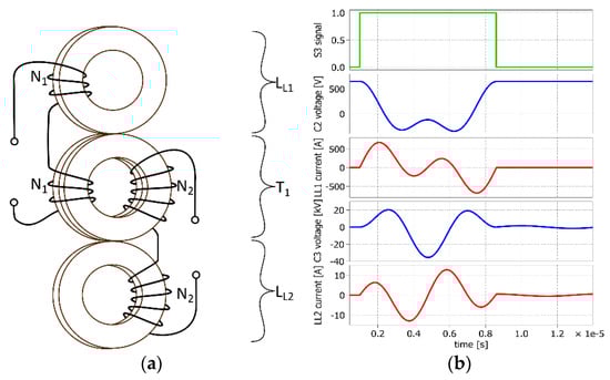
Figure 5.
(a) A cored Tesla transformer construction concept with leakage inductances LL1, LL2, and the main magnetizing part T1; (b) the output pulse shaping unit simulation results, from the top: switch S3 control signal, C2 capacitor voltage, switch current, C3 capacitor voltage and current.
Proper selection of the number of cores and magnetic properties of magnetic cores led to a defined magnetic coupling. In the constructed prototype, seven cores were used in a 2–3–2 arrangement, which led to the desired k = 0.6 coupling coefficient. The term 2–3–2 means that two cores were used for primary side leakage inductance LL1, three cores were used for main part of the transformer T1, and two cores were implemented for secondary side leakage inductance LL2 of the design transformer. The different numbers and properties of the cores and their proper arrangement allows for reaching any defined magnetic coupling ratios, such as k = 0.6(6), k = 0.75, k = 0.8, k = 0.9, etc. This design idea could be easily implemented in LLC DC/DC converter design to simplify the magnetics.
An important aspect of the design was to use the same magnetic core material for leakage inductances and the main transformer. This means that the system will be using the same part of the magnetic hysteresis loop of the material to maintain a constant coupling ratio during transformer operation. For the same reason, the number of primary windings, N1 (windings of the primary leakage inductance and primary side of the transformer), should be equal. Similarly, N2 (for secondary leakage inductance and secondary side of transformer) should be equal.
The prototype was built with seven MS-250026-2 micrometal cores with a reduced magnetic permeability of μr = 60. The primary winding is made of 64 coils connected in parallel. Each of these coils were made as a single turn of ~1 mm2 litz wire. The secondary winding is made of 50 turns of the same litz wire that was used in the primary side. The cores and windings of the primary leakage inductance and primary side of the transformer were insulated by epoxy resin impregnation. Figure 6 shows the transformer components before the final assembly and the main transformer part mounted with the primary leakage inductance and the primary windings.
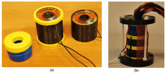
Figure 6.
(a) The magnetic transformer parts and (b) the transformer with mounted primary windings.
Due to high current amplitudes on the primary side of the transformer, eight parallel 1200 V, 100 A IXA70I1200NA IXYS IGBTs and eight 1200 V, 20 A CoolSiC™ IDH20G120C5 Infineon antiparallel diodes were used. Alike C2, the C3 capacitance is made of 50 WIMA FKP 10 nF capacitors connected in parallel, due to the high voltage amplitudes on the output of the power supply. The S3 switching module and the C3 output capacitor bank are presented in Figure 7.
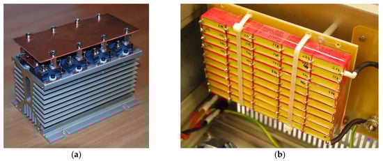
Figure 7.
(a) The S3 switching module (8 IGBTs (Isolated Gate Bipolar Transistors) and 8 SiC antiparallel diodes are under the copper busbar visible at the top); (b) the C3 output capacitance.
The power supply load for a DBD or CD plasma reactor is to be connected in parallel to the C3 capacitance; hence, to achieve the best energy transfer efficiency, the reactor capacity should be taken into account in the power supply design, especially in case of DBD reactors that exhibit large internal capacity.
3. Results
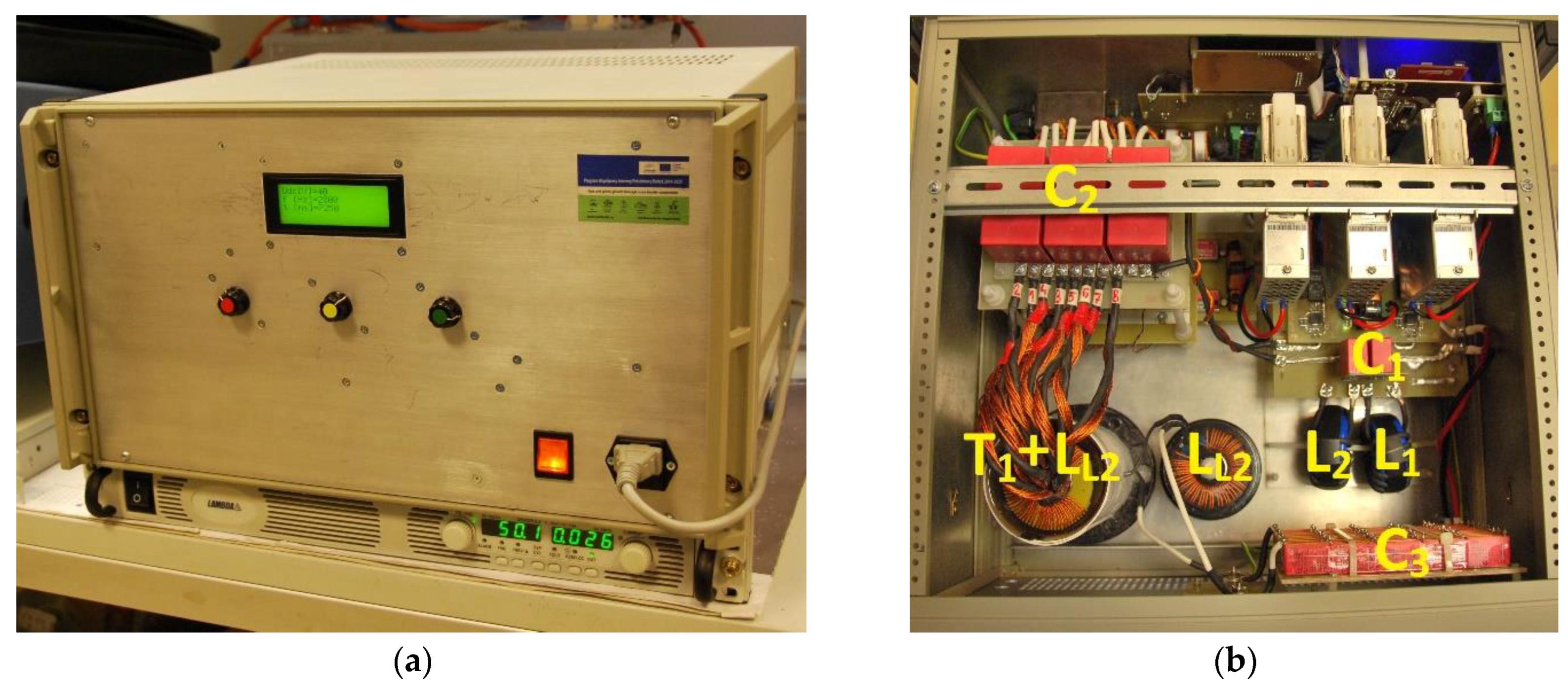
The constructed prototype of the high-voltage pulsed power supply, implementing SiC technology and the Tesla coil-like transformer design, is depicted in Figure 8.

Figure 8.
(a) The constructed high-voltage power supply prototype and (b) its main internal components (equivalent circuit component names).
All of the waveforms presented below were recorded using the LeCroy WaveRunner 6100A digital oscilloscope. The voltages on C1 and C2 were measured using a passive Tektronix P5100A probe, and the currents on L1 and L2 were measured using LeCroy CP031 Hall effect current probes. The output voltage was measured using a passive Tektronix P6015A high-voltage probe. The current on the primary and secondary side of transformer was measured using a type 6585 current monitor by Pearson.
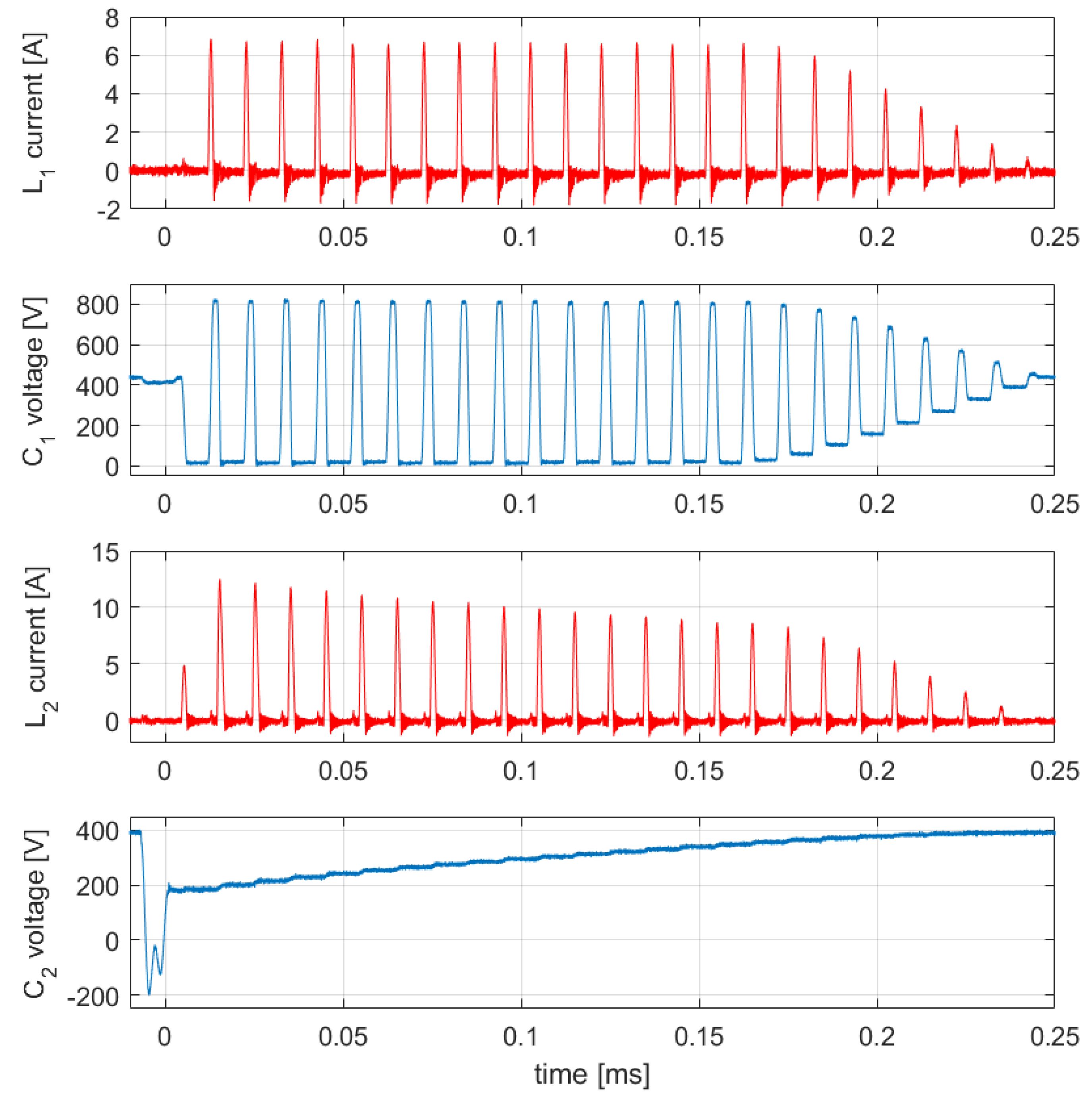
Figure 9 presents voltage and current waveforms for C and L elements of the resonant capacitor charger unit. The presented waveforms were recorded for 400 V of input voltage and under high load conditions. The charging process started at time zero, just after the previous output pulse generation process was finished. During normal operation, the initial voltage across capacitor C2 did not drop to zero because the unused energy from the output pulse generation process always recharge it. To charge the capacitor C2 from 0 V to its final voltage (400 V) 30 repetitions were needed, while in normal operation (under lighter loads), the typical number of repetitions was around 15–20.
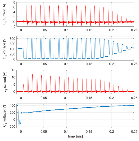
Figure 9.
The measured voltage and current waveforms of capacitor resonant charger (measured at main L and C components—refer to Figure 2).
In the worst case (the lowest initial voltage of C1 and highest amplitude of inductor L1 current) the efficiency of energy transfer from DC voltage source to capacitor C1 was above 98%. With the same efficiency, the energy was transferred from capacitor C1 to C2. The overall efficiency of the resonant capacitor charger unit was typically higher than 96%.
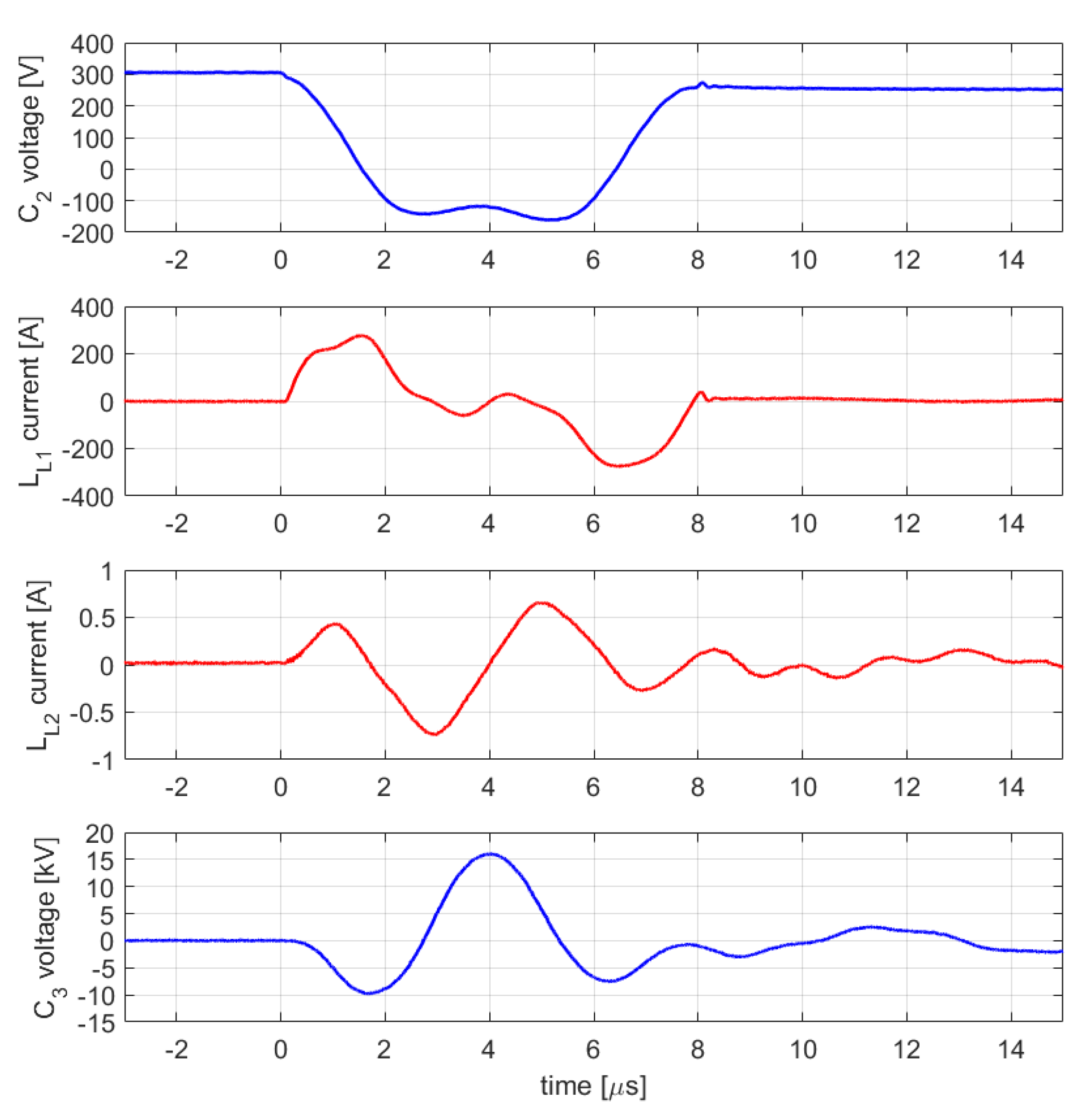
Figure 10 shows voltage and current waveforms of the output pulse shaping circuitry. The waveforms were recorded for 300 V of input voltage (for higher voltage values, energy consumption in the load significantly affects current waveforms). The process started at time zero, when the capacitor C2 was charged to its initial value. After switching S3 on, the energy stored in capacitor C2 was transferred through the transformer’s magnetic circuit to the capacitor and parallel-connected load, either a DBD or PCD reactor. For 400 V of input voltage, the amplitude of the generated high-voltage pulse was around 20 kV, due to the high transformer winding ratio (n = 50). Any energy which was not consumed in the load for gas ionization backflowed to capacitor C2.
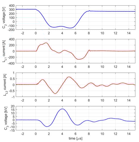
Figure 10.
The voltage and current waveforms of the high-voltage pulse shaping unit.
For an ideal circuit, the current pulses should be quasi-sinusoidal. Distortions, especially visible in the current of the primary side of the transformer, were caused by the parasitic capacitances of transformer windings [17].
The energy transfer efficiency from C2 to C3 was above 84% and, therefore, the whole process of output pulse generation (energy transfer from C2 to C3 and back from C3 to C2) was achieved with an efficiency of about 71%.
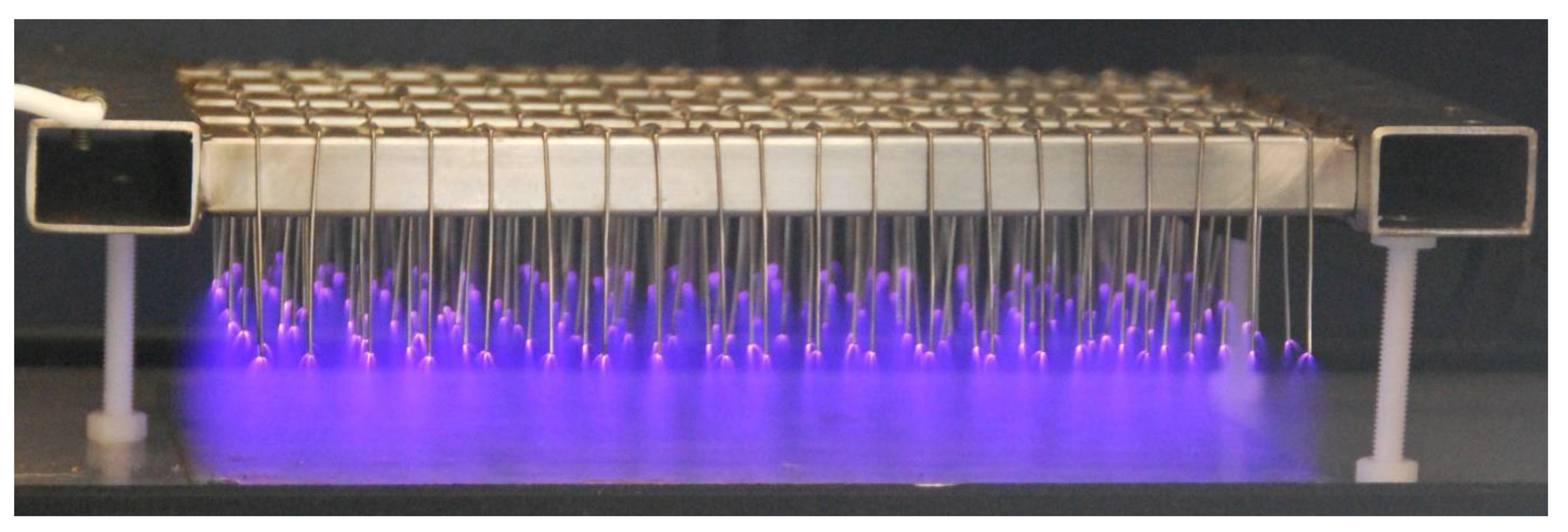
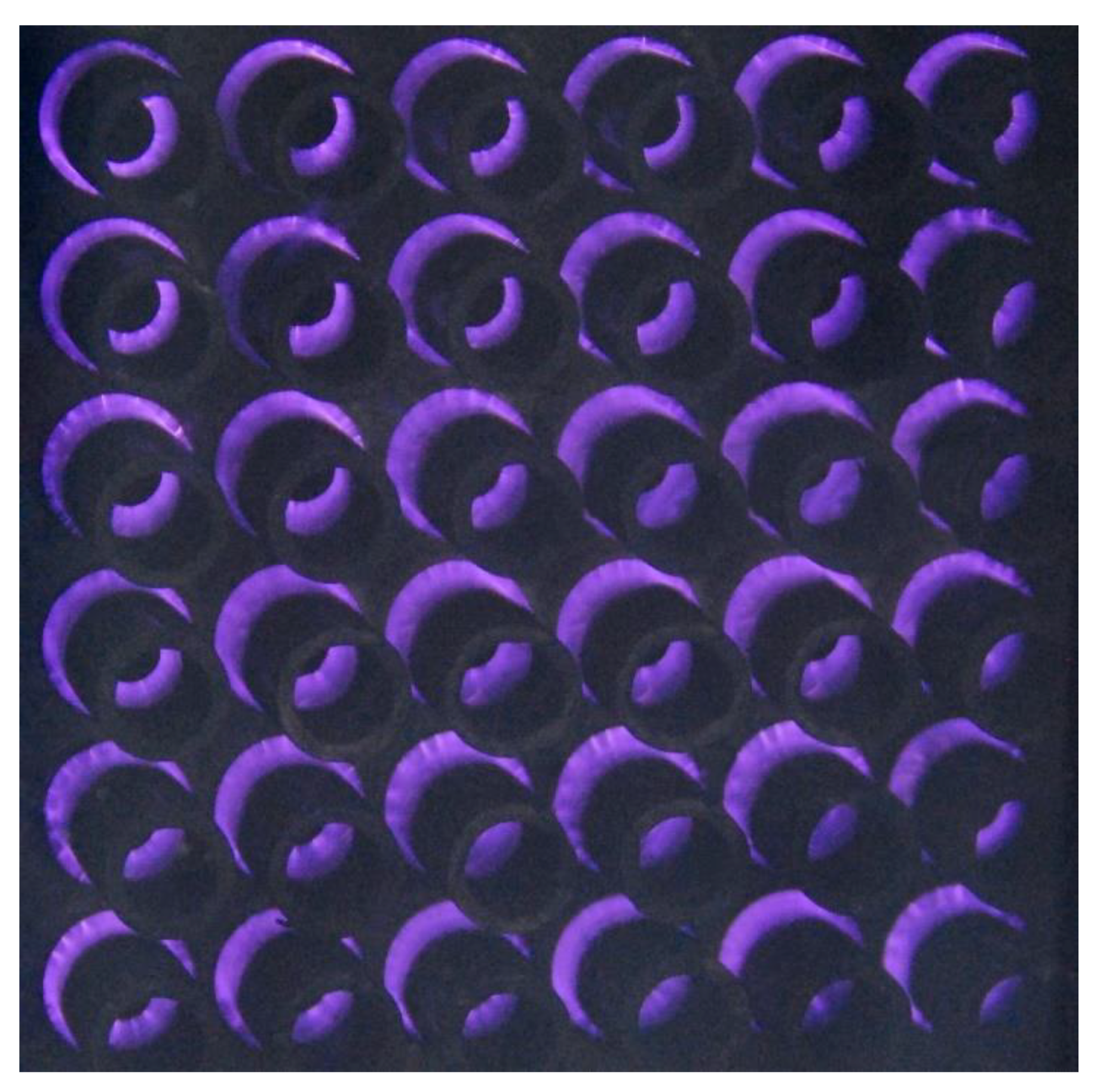
To test the prototype in real application conditions, two types of loads were used. At first, a PCD reactor was created as a matrix of HV electrode needles above the low-potential flat metal plate. The electrical capacity of the reactor was 27 pF. Figure 11 shows the typical discharge formation during operation.

Figure 11.
PCD reactor supplied by the high-voltage pulsed power supply proposed in this work.
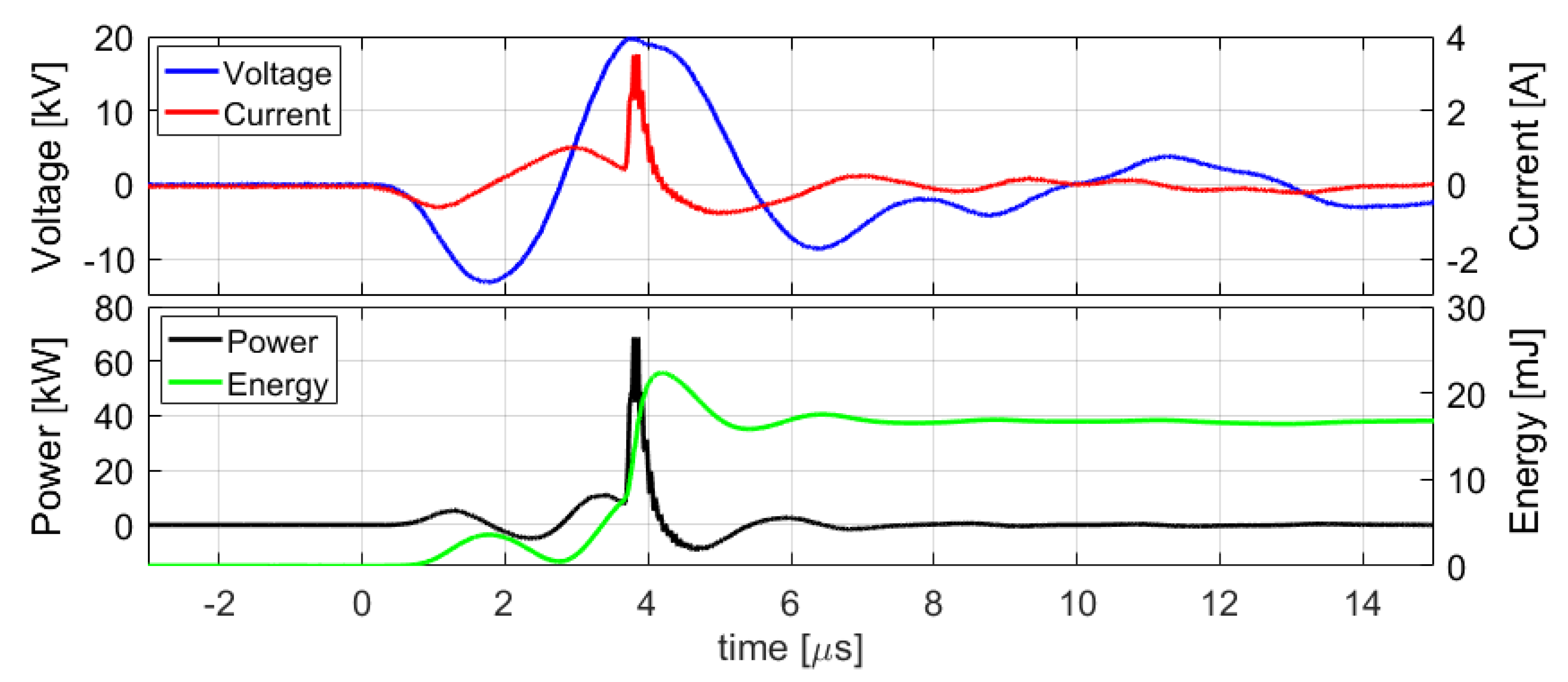
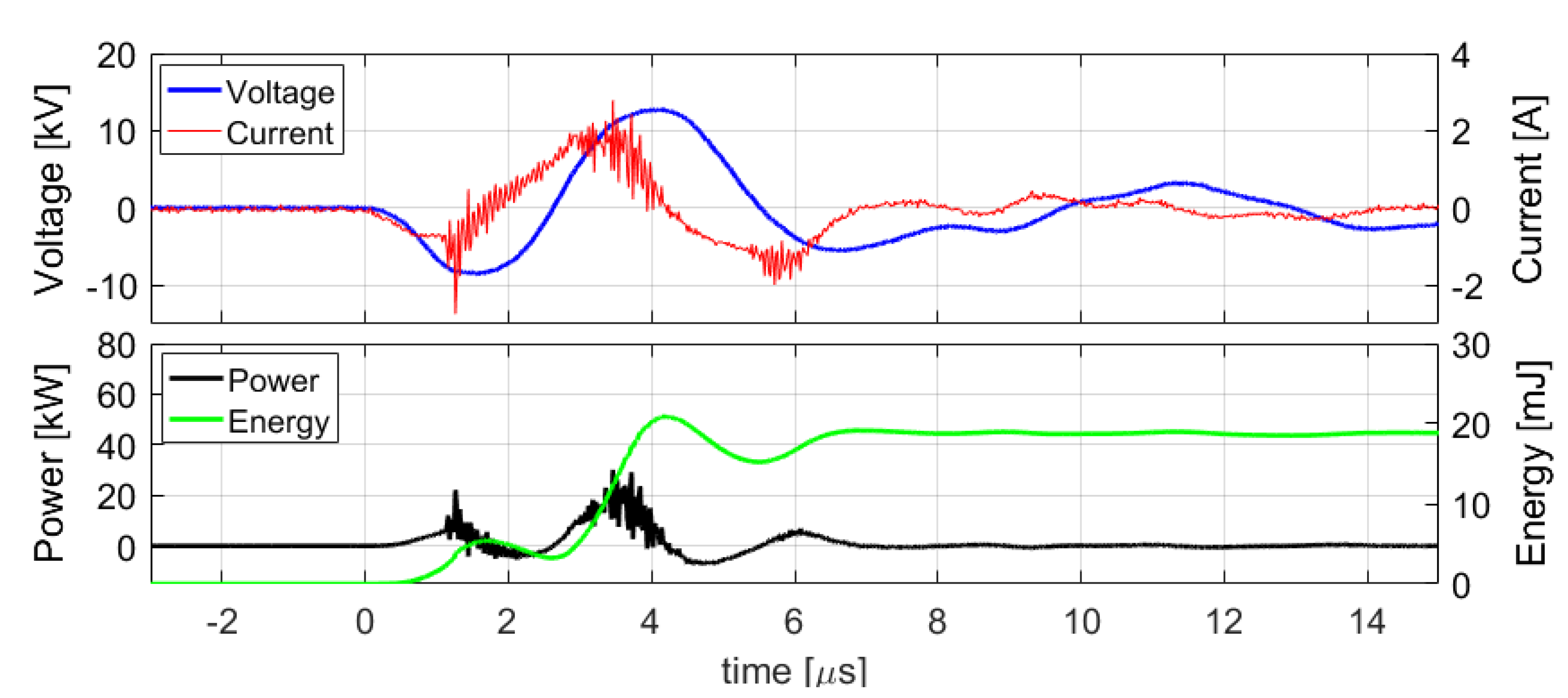
Figure 12 shows the typical voltage and current waveforms of a PCD reactor discharge and calculated power and energy applied to the load. The corona discharges take place at the maximum value of the voltage (peak of ~20 kV); therefore, the current waveform has two components. First, coming from the capacity of the reactor and capacitance of C3 (shaped by resonance of the output circuit). Second, as the current peak connected with electrical discharges in the reactor [18].
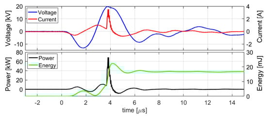
Figure 12.
The measured output voltage and current waveforms for PCD reactor discharge and calculated discharge power and energy.
As a second type of load, a DBD-type reactor was used as shown in Figure 13. Cylindrical, metal electrodes of the reactor are separated with dielectric tubes made of Al2O3 (aluminum oxide). The discharge matrix consists of 36 identical discharge tubes. The total capacitance of the reactor was 65 pF.

Figure 13.
The dielectric barrier discharge (DBD) reactor supplied by the proposed power supply prototype.
The measured waveforms for a DBD-type load are presented in Figure 14. The reactor current—plotted in red, such as in the case of PCD—consists of two components, namely, the reactor and the C3 capacitance current. For a DBD, the discharge current is typically made of many current peaks of short time (nanosecond range) [19]. The much smaller distance between electrodes causes the discharge to take place at much lower voltages (~8 kV) and its duration covers most of the time of the output voltage pulse.

Figure 14.
The measured output voltage and current waveforms for PCD reactor discharge and calculated power and energy applied to the load.
4. Discussion
The proposed high-voltage power supply topology was designed for capacitive types of load. This feature makes it suitable to supply non-thermal plasma reactors of various constructions. While most high-voltage power supplies are designed to supply only one type of load with a specified capacity [8,9], the proposed topology is appropriate for both DBD and PCD plasma reactors, and for a wide range of reactor capacities. The construction is fully resonant, with all the used semiconductor switches being commutated in ZCS (zero current switching) mode in order to limit switching loss. SiC technology was used to increase the efficiency of consecutive converters. Usually, in the case of high-voltage pulsed converters, control of semiconductor switches demands high precision and additional feedback (e.g., voltage or current sensing circuits) is often used [20]. An important feature of the proposed converter is loss minimization due to soft switching of power switches regardless of changes in the load, so there is no need to use additional feedbacks and/or additional snubbers or other switch protection circuits. The mentioned feature also significantly simplifies the power supply control algorithms.
The resonant capacitor charger unit allows for recharging of the energy storage capacitor with a high efficiency and provides the additional possibility to adjust its final voltage value by regulation of the charging interval number. The efficiency of the charging process was 96%.
The presented high-voltage transformer design is scalable to various transformer winding ratios and magnetic coupling ratios through proper selection of the number and arrangement of magnetic cores used in the design. The proposed transformer construction allows for obtaining low magnetic coupling between transformer windings along with a small external magnetic field. The energy conversion efficiency of the constructed transformer prototype was similar or higher compared to similar constructions [14,21], but the EMC (electromagnetic compatibility) was significantly increased.
The disadvantage of the proposed topology is the high current amplitude on the primary side of the transformer, however, this a typical feature of this group of converters [14].
The output pulse was shaped by resonance of the high-voltage transformer leakage inductances and the capacitance of the load. In the case of small capacitance reactors (e.g., a PCD reactor with wide discharge gaps) additional capacitance, C3, is connected in parallel to the load, and helps to stabilize the resonance conditions. In the case of reactors exhibiting big capacitance (e.g., large area DBD reactors) capacitance C3 can be omitted, and only the capacity of the reactor will affect the resonance frequency. To maximize the efficiency, the reactor capacitance should be taken into account in converter design. The power delivered to the load can be regulated by both the regulation of output pulse amplitudes and their repetition frequency. The maximum frequency of output pulse generation of the built prototype was 2 kHz, and the maximum voltage amplitude was 20 kV for 400 V of input DC voltage bus. The efficiency of the output pulse generation process for the pulse shaping unit was 71%, which is a good result considering that the applied high-voltage transformer had a large number of secondary windings and several magnetic cores.
The output pulse shaping unit utilizes the principles of a Tesla coil transformer and the natural resonance of the circuit created by the transformer’s parasitic inductances and a capacitive load. The shape of the output voltage pulse was asymmetric, and its average value was equal to zero, which is beneficial for DBD reactors. After pulse formation, the energy unused for discharge generation backflows to the converter and results in low residual oscillations and low residual energy stored in the reactor dielectric barrier capacitance, which usually causes the rise of reactor temperature and decreases plasma generation efficiency.
The operation of the power supply was successfully presented for both PCD and DBD, and the most common plasma reactor constructions. Interestingly, although both discharge regimes were different and took place at different voltage levels, the energy per cycle was similar, and slightly below 20 mJ.
5. Patents
The power supply construction elements were patented with priority numbers P.427673 and P.429151.
Author Contributions
Conceptualization: J.K. and M.H.; validation: J.K.; resources: M.H. and J.K.; data curation: J.K.; writing—original draft preparation: J.K. and M.H.
Funding
This research was partly funded by the European Union Interreg South Baltic Programme “Sludge Technological Ecological Progress—increasing the quality and reuse of sewage sludge” number STHB.02.02.00-32-0110/17; project acronym: STEP.
Acknowledgments
The authors would like to thank Stanislaw Kalisiak for his inspiration and fruitful discussions as well as Ludwik Bojański for technical assistance during measurements and prototype preparation.
Conflicts of Interest
The authors declare no conflict of interest.
References
- Ohta, T. Plasma in agriculture. In Cold Plasma in Food and Agriculture; Misra, N.N., Schluter, O., Cullen, P.J., Eds.; Academic Press: Waltham, MA, USA, 2016; Chapter 8; pp. 205–221. ISBN 9780128013656. [Google Scholar]
- Metelmann, H.-R.; von Woedtke, T.; Weltmann, K.-D. Cold physical plasma for medical application. In Comprehensive Clinical Plasma Medicine; Springer International Publishing: New York, NY, USA, 2018. [Google Scholar]
- Inhwan, H.; Jongku, J.; Taesuk, Y.; Jinmu, J. Water electrode plasma discharge to enhance the bacterial inactivation in water. Biotechnol. Biotechnol. Equip. 2018, 32, 530–534. [Google Scholar] [CrossRef]
- Weltmann, K.-D.; Kolb, J.F.; Holub, M.; Uhrlandt, D.; Simek, M.; Ostrikov, K.K.; Hamaguchi, S.; Cvelbar, U.; Cernak, M.; Locke, B.; et al. The future for plasma science and technology. Plasma Process Polym. 2018, 16, e1800118. [Google Scholar] [CrossRef]
- Schmidt, M.; Holub, M.; Jogi, I.; Sikk, M. Treatment of industrial exhaust gases by a dielectric barrier discharge. Eur. Phys. J. Appl. Phys. 2016, 75, 24708. [Google Scholar] [CrossRef]
- Brandenburg, R.; Bogaerts, A.; Bongers, W.; Fridman, A.; Fridman, G.; Locke, R.B.; Miller, V.; Reuter, S.; Schiorlin, M.; Verreycken, T.; et al. White paper on the future of plasma science in environment, for gas conversion and agriculture. Plasma Process Polym. 2018, 16, e1700238. [Google Scholar] [CrossRef]
- Wala, A.S.; Aymen, A.A.; Monia, G.; Bouzaza, A.; Aboussaound, W.; Soutrel, I.; Ouederni, A.; Wolbert, D.; Rtmini, S. Abatement of ammonia and butyraldehyde under non-thermal plasma and photocatalysis: Oxidation processes for the removal of mixture pollutants at pilot scale. Chem. Eng. J. 2018, 344, 165–172. [Google Scholar] [CrossRef]
- Wang, D.; Namihira, T.; Akiyama, H. Pulsed discharge plasma for pollution control. In Air Pollution; InTech: London, UK, 2010. [Google Scholar]
- Kolek, J.; Jakubowski, T.; Balcerak, M. Impact of voltage shape on efficiency of ozone generation. In Proceedings of the 19th European Conference on Power Electronics and Applications (EPE’17 ECCE Europe), Wasaw, Poland, 11–14 September 2017. [Google Scholar]
- Brandenburg, R. Dielectric barrier discharges: Progress on plasma sources and on the understanding of regimes and single filaments. Plasma Sources Sci. Technol. 2017, 26, 053001. [Google Scholar] [CrossRef]
- Kolek, J.; Kalisiak, S.; Holub, M. Resonant, high voltage power supply for non-thermal plasma reactors. WZEE 2018, in press. [Google Scholar]
- Denicolai, M. Optimal performance for Tesla transformers. Rev. Sci. Inst. 2002, 73, 1–5. [Google Scholar] [CrossRef]
- Liu, Y.; Lee, L.; Bing, Y.; Ge, Y.; Hu, W.; Lin, F. Resonant charging performance of spiral tesla transformer applied in compact high-voltage repetitive nanosecond pulse generator. IEEE Trans. Plasma Sci. 2013, 41, 3651–3658. [Google Scholar] [CrossRef]
- Balcerak, M.; Jakubowski, T.; Kalisiak, S. Compact pulsed power supply based on Tesla transformer for plasma reactors. In Proceedings of the 19th European Conference on Power Electronics and Applications, Warsaw, Poland, 11–14 September 2017; pp. 1–9. [Google Scholar]
- You, B.G.; Kim, J.S.; Lee, B.L.; Choi, G.B.; Yoo, D.W. Optimization of powder core inductors of buck-boost converters for hybrid electric vehicles. J. Electron. Eng. Technol. 2011, 6, 527–534. [Google Scholar] [CrossRef]
- Kralj, L.; Miljavec, D. Stray losses in power transformer tank walls and construction parts. In Proceedings of the The XIX International Conference on Electrical Machines—ICEM, Rome, Italy, 6–8 September 2010; pp. 1–4. [Google Scholar]
- Williams, D.M. Self-capacitance of high-voltage transformers. IEEE Trans. Power Electron. 2017, 22, 22–26. [Google Scholar]
- Kim, Y.; Cha, M.S.; Shin, W.; Song, Y. Characteristics of dielectric barrier glow discharges with a low-frequency generator in nitrogen. J. Korean Phys. Soc. 2003, 43, 732–737. [Google Scholar] [CrossRef]
- France, P.I.V.; Abb, E. Dielectric-barrier discharges principle and applications. Plasma Processes Polym. 1997, 7, C447–C466. [Google Scholar]
- Pokryvailo, A.; Carp, C.; Scapellati, C. A high-power high_voltage power supply for long-pulse applications. IEEE Trans. Plasma Sci. 2010, 38, 2604–2610. [Google Scholar] [CrossRef]
- SooWon, L.; ChuHyun, C.; Hong-Je, R.; Jong-Soo, K.; Geun-Hie, R.; Yun-Sik, J. Fabrication andoperation testing of a dual resonance pulse transformer for PFL pulse Charging. J. Korean Phys. Soc. 2011, 59, 3679–3682. [Google Scholar]

© 2019 by the authors. Licensee MDPI, Basel, Switzerland. This article is an open access article distributed under the terms and conditions of the Creative Commons Attribution (CC BY) license (http://creativecommons.org/licenses/by/4.0/).