Article

Optical, Electrical, and Surface Properties of Cu/Plasma Polymer Fluorocarbon Nanocomposite Thin Film Fabricated Using Metal/Polymer Composite Target

Chemical Materials Solutions Center, Korea Research Institute of Chemical Technology, Daejeon 34114, Korea
*
Author to whom correspondence should be addressed.
Appl. Sci. 2019, 9(7), 1296; https://doi.org/10.3390/app9071296
Submission received: 27 February 2019 / Revised: 22 March 2019 / Accepted: 26 March 2019 / Published: 28 March 2019
(This article belongs to the Special Issue Cold Atmospheric Plasma: Sources, Processes, and Applications)

Abstract

:
We propose a new method of fabricating metal–polymer composite targets for sputtering, which makes it easier to control the composition and enables the homogeneous and reproducible fabrication of metal–polymer nanocomposites over large areas. Using Cu/polytetrafluoroethylene composite targets containing 20, 50, and 80 wt.% Cu, Cu/plasma polymer fluorocarbon (PPFC) nanocomposite thin films were prepared by radio-frequency (RF) sputtering. Targets with 80 wt.% Cu were conductive; moreover, sputtering was possible not only with RF but also with mid-range frequency (MF) and direct current (DC) power sources. The nanocomposite thin film deposited by MF and DC power using an 80 wt.% Cu target showed near-metallic characteristics, exhibited absorption peaks at 618 and 678 nm, and had a surface resistance of 2 × 10⁴ and 34.55 Ω/sq, respectively. We also analyzed the structure and composition of the Cu/PPFC nanocomposite films by X-ray diffraction and X-ray photoelectron spectroscopy. The described metal–polymer targets can advance the applications and commercialization of nanocomposite thin films.

1. Introduction

Polymer–metal nanocomposites exhibit excellent optical [1,2,3,4,5,6,7,8], electrical [1,4], and mechanical properties [9,10] and have been attracting much attention owing to their various characteristics such as surface hardness [6], bioactivity [11,12], perfect absorbance, [13,14,15], and sensing ability [16]. Polymers with good insulating properties are well suited as host materials for supporting a variety of metal clusters [5,17]. The excellent properties of polymer–metal nanocomposites depend on the size, quantity, and shape of various metal clusters contained in the polymer matrix; various studies elucidating these properties have been performed [17,18], with reference to surface antimicrobials and abrasion-resistant coatings, and gas sensor films [19,20,21,22].
As a polymer matrix, polytetrafluoroethylene (PTFE), which is mechanically, thermally, and chemically stable, and has excellent insulation and optical properties, is widely used [1,3,6,9,11,19,23]. Studies using noble metals such as Ag [5,9,11,19,24,25,26], Au [3,16,27], and Cu [12,13,14] have been carried out, but mostly, Ag and Au have been used. In addition to noble metals, nanocomposites using SiO2 [6], graphite [10], ZnO [19], Ti [28], Fe–Ni–Co [29], and TiO2 [30], with PTFE, have also been reported.
A nanocomposite can be fabricated by the physical vapor deposition (PVD) method, as PVD allows for control of the dopant, enables uniform coating, and minimizes the reaction with air. The co-sputtering method employing two sputtering cathodes [3,6,9,10,12,13,14,19,28] is the most widely used method, and other methods involve the use of an evaporator [9,25], sputter evaporator, ion beam co-sputtering [16], and pulsed laser deposition [24], to fabricate a polymer–metal nanocomposite. However, the use of two sputtering cathodes or a combination of two deposition methods to fabricate nanocomposites requires precise control for yield matching; moreover, it is difficult to ensure reproducibility of the experimental results owing to the complicated equipment configuration and difficulty in securing uniformity over a large area, which are stumbling blocks toward commercialization.
In a previous study, our group found that a plasma polymer fluorocarbon (PPFC) thin film prepared using a carbon nanotube (CNT)/PTFE composite sputtering target exhibited diverse physical properties depending on the content of the CNT. In addition, it has been reported that CNT, when added to a composite target, imparts conductivity; hence, sputtering is also possible using a mid-range frequency (MF) power source [31]. Taking our previous study forward, in this study, a Cu/PTFE composite target for sputtering was first introduced for fabricating a Cu/PPFC nanocomposite thin film by uniformly dispersing Cu metal powder in PTFE powder and pressing at high temperature. Previously, the composite target was prepared by attaching half of the polymer target to half of the metal target, or attaching a metal foil or wire to the surface of the polymer target [1,6]. However, in those studies, it was challenging to deposit a nanocomposite thin film of uniform composition ratio over a large substrate area and prepare a reproducible target; therefore, practical composite targets have been difficult to achieve thus far. We fabricated noble polymer–metal composite targets with 20, 50, and 80 wt.% Cu in PTFE powder. Thus, the filling ratio of the metal nanoclusters in the nanocomposite thin film can be easily controlled, and the nanocomposite thin film can be prepared by long-duration sputtering with one target in the same manner as the conventional sputtering target, enabling excellent reproducibility. Finally, because of the controllability and simple equipment configuration, large-area sputtering is possible; hence, this method can be employed in a wide variety of polymer–metal nanocomposite technical and commercial applications.
In this study, we investigated the physical and chemical properties of the Cu/PPFC nanocomposite thin films with various Cu contents, and analyzed how the properties of the films change with radio-frequency (RF), MF, and direct current (DC) power sources using the Cu/PTFE (20:80, w/w) target.

2. Materials and Methods

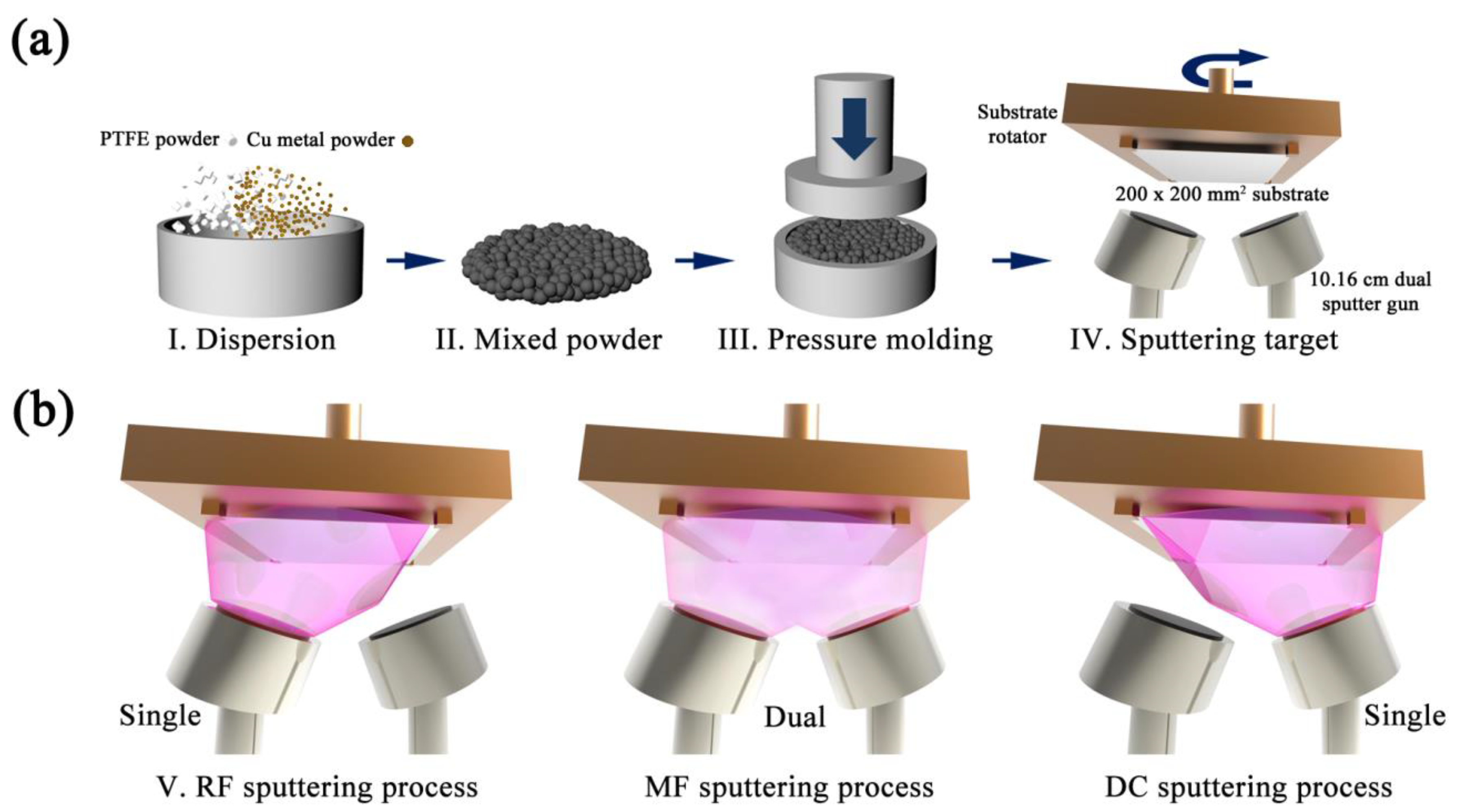
2.1. Preparation of Cu/PTFE Composite Sputtering Targets

Cu powder (e-Cu25, Chang Sung) was mixed with PTFE powder (A7, DuPont) at weight ratios of 20:80, 50:50, and 80:20, respectively, following which composite sputtering Cu/PTFE targets were prepared by a high-temperature compression molding method. Compression pressure was 200 kgf/cm2 and molding temperature was 370 °C. A pure PTFE sputtering target devoid of any Cu powder was also prepared by the same method for reference. Disk-type Cu/PTFE composite sputtering targets with a diameter of 10.16 cm and thickness of 0.64 cm were then fabricated by milling. For simplicity, the targets were labeled PTFE (Cu 0), Cu 20, Cu 50, and Cu 80 according to the composition ratio. Figure 1a sequentially shows the fabrication of the Cu/PTFE composite target.

2.2. Fabrication of Cu/PPFC Nanocomposite Thin Films

The sputtering chamber was evacuated to a base pressure of 6.6 × 10⁻³ Pa by a mechanical pump and a cryogenic pump. The partial pressure of Ar during the process was 0.93 Pa. The Cu/PPFC nanocomposite thin films were fabricated using RF (13.56 MHz), MF (40 kHz), and DC power with a sputtering power density of 1.23 W/cm2. Dual magnetron cathodes were used for MF sputtering to improve sputtering efficiency. Target-to-substrate distance was fixed at 24 cm. A schematic diagram of the sputtering process for each power source is shown in Figure 1b. We used a polyethylene terephthalate (PET, KIMOTO, Japan) film substrate of size 20 × 20 cm2 and thickness 125 μm. In order to compare the physical properties of the thin films with different Cu composition ratios, pure PTFE, Cu 20, Cu 50, and Cu 80 composite targets were sputtered with an RF power source to fabricate the thin films. Deposition rates for each composite target and sputtering power source were determined by using the Alpha step method (Dektak XT, Bruker, MA, USA). A thickness step is generated by covering a part of the sample for measurement. To investigate the physical properties of the Cu/PPFC nanocomposite thin films according to power source, 100 nm thin films were fabricated by sputtering with RF, MF, and DC power sources using the Cu 80 composite target. The fabricated thin films were named “target name + power source type” for clarity and conciseness. For example, a thin film made by an RF power source using a Cu 20 composite target is named “Cu 20 RF”, whereas that made by a DC power source using a Cu 80 composite target is named “Cu 80 DC”.

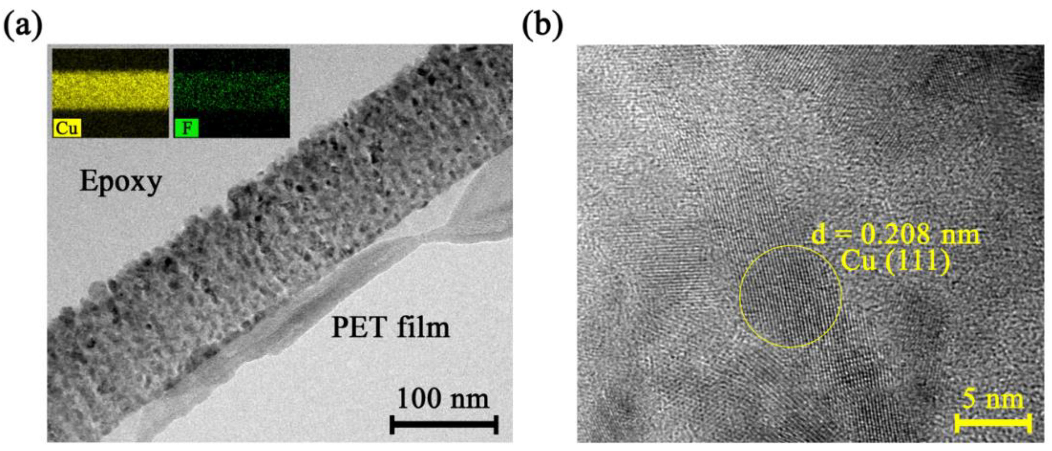
2.3. Characterization of Cu/PPFC Nanocomposite Thin Films
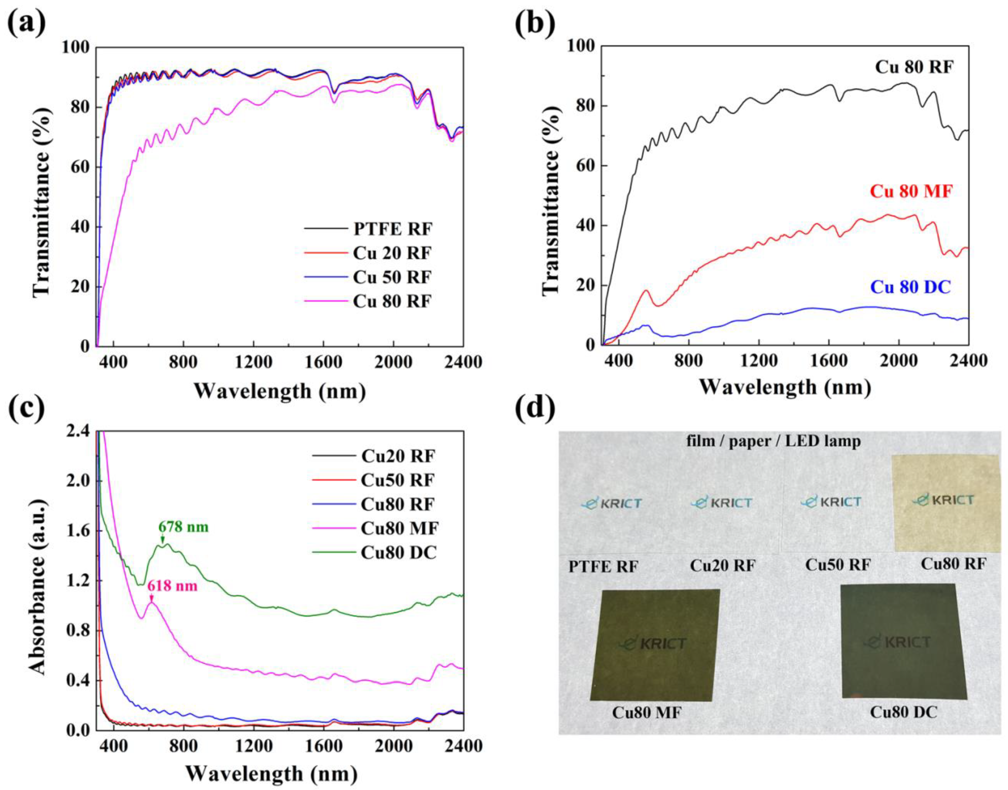
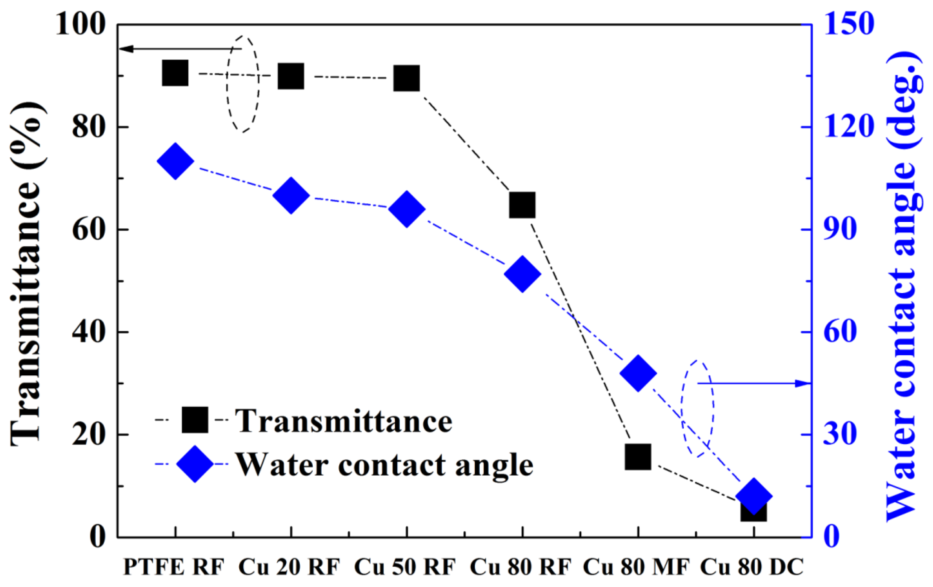
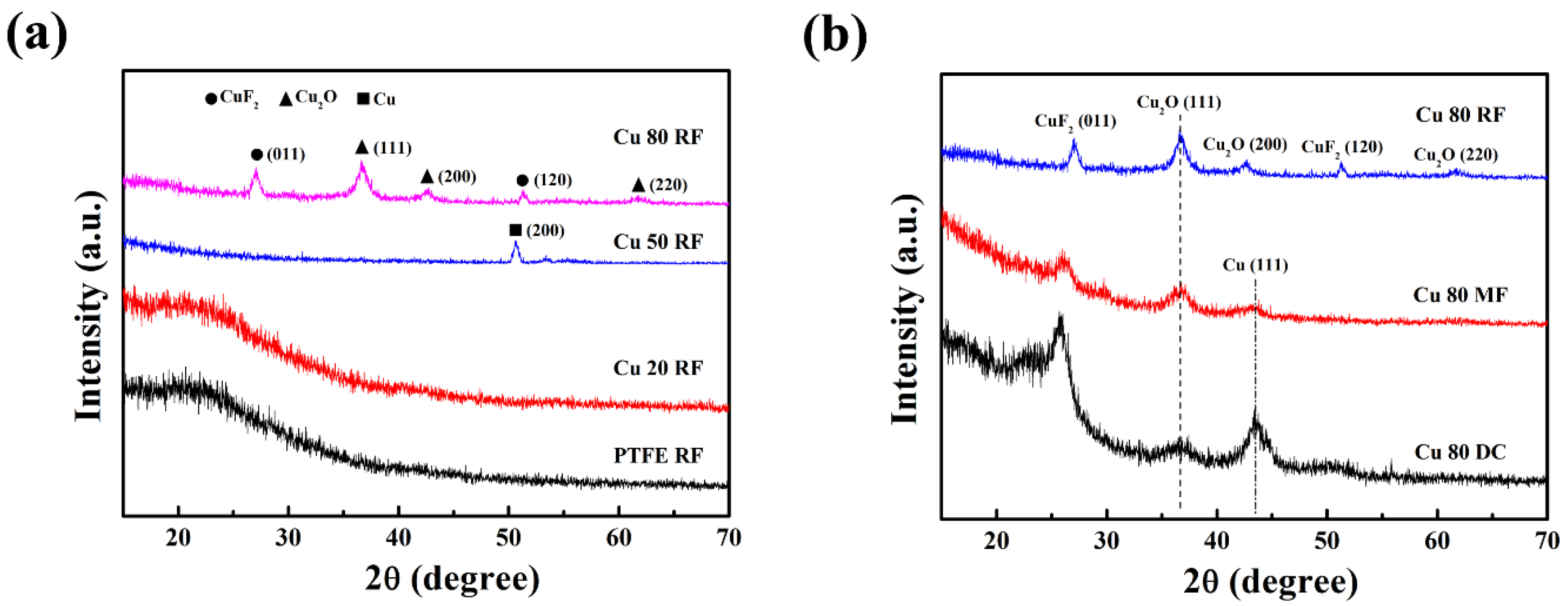
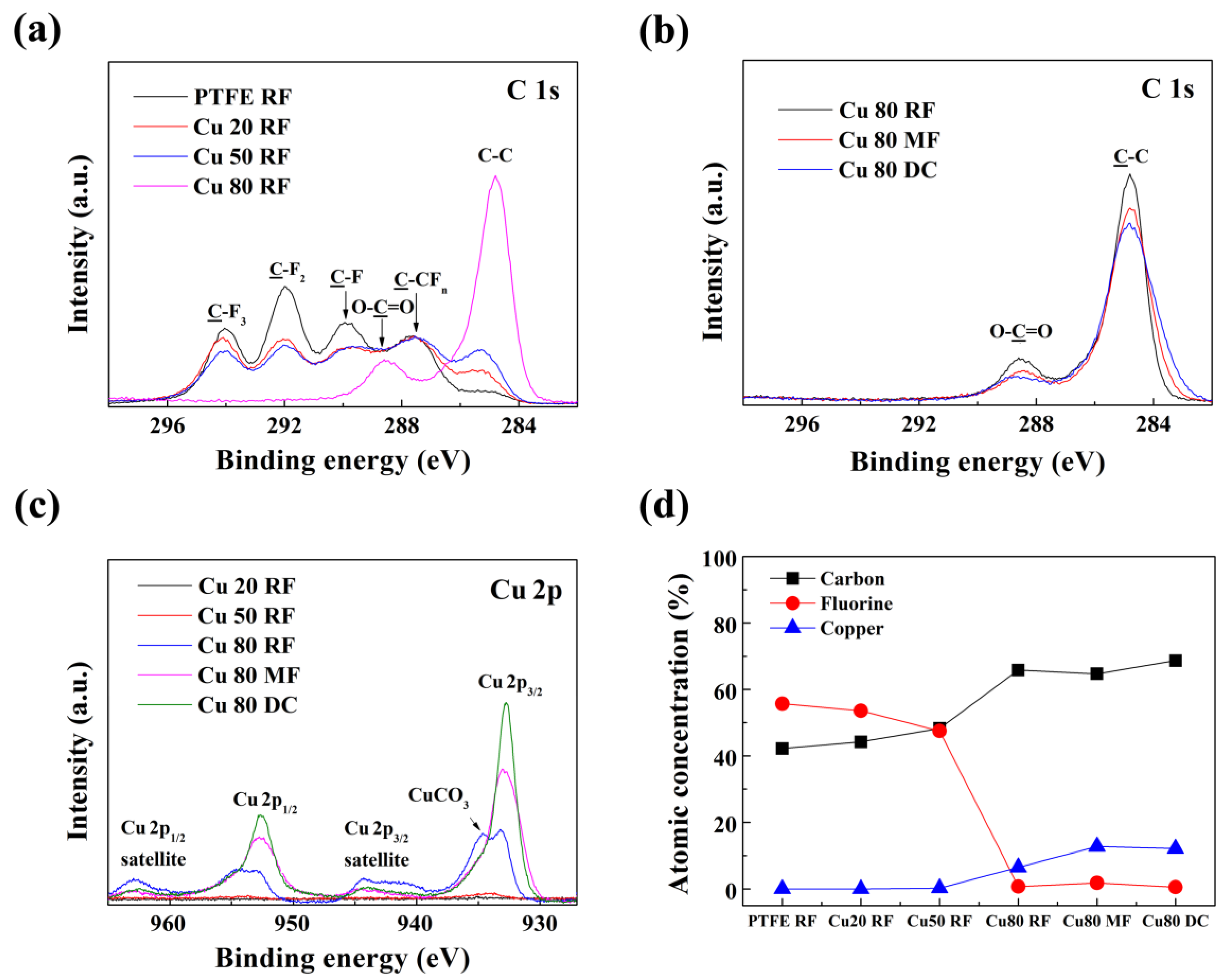
The nanocomposite structure of Cu/PPFC thin film was investigated by field-emission transmission electron microscopy (FE-TEM, Tecnai G2 F30 S-Twin, FEI Co., Hillsboro, OR, USA). Optical properties of the thin films were measured by UV–VIS spectroscopy (U-4100, Hitachi, Tokyo, Japan). Standard deviation of water contact angle, sheet resistance, optical transmittance, and b* (yellow index) were measured by five points at each sample. The measuring points were the center and four sides of the film. The surface energy of the nanocomposite thin film was measured using a contact angle analyzer (Phoenix 300 Touch, Surface Electro Optics, Suwon, Korea). The volume of water droplets was 2 μL, and the images were automatically analyzed by the system. Structural characteristics of the Cu/PPFC nanocomposite thin films were analyzed by X-ray photoelectron spectroscopy (XPS, AXIS Nova, Kratos, Manchester, UK) and X-ray diffraction (XRD, SmartLab, Rigaku, Tokyo, Japan).

3. Results

The Cu 20 and Cu 50 composite targets showed no electrical conductivity, while the Cu 80 targets showed a good sheet resistance of 2.1 × 10⁻³ Ω/sq. Therefore, first, the nanocomposite thin film was fabricated using an RF power source, and the change in the physical properties of the thin film according to the Cu composition in the composite target was investigated. Figure 2a shows a cross-sectional TEM image of the Cu 80 MF thin film. The inserted element mapping image displays homogenous distribution of copper and fluorine atoms in the thin film. Cu metal nanoclusters were distributed in a spherical shape with a size of 10–20 nm. Figure 2b shows a lattice of nanocluster Cu in PPFC thin film matrix. The central Cu nanocluster domain, which is marked yellow, shows (111) plane orientation with a lattice distance of 0.208 nm. In this TEM image, we confirmed that Cu nanoclusters were well formed as a crystalline phase in the plasma polymer fluorocarbon matrix.
Figure 3 shows the optical properties for a 100 nm thick Cu/PPFC nanocomposite thin film. Figure 3a shows the optical transmittance graph of the Cu/PPFC nanocomposite thin film deposited by RF sputtering. For comparison, the results for the thin films deposited using a pure PTFE target devoid of Cu are also shown. The optical properties of the Cu 20 RF and Cu 50 RF nanocomposite thin films were very similar to those of PTFE RF thin films. They exhibited a high transmittance of 90% or more in the visible light region and showed excellent transmission characteristics even in the infrared (IR) region. For the Cu 80 RF thin film, visible light transmittance was drastically decreased, and the transmittance was about 70% at a wavelength of 500 nm. As the Cu content increased, the characteristics of Cu in the nanocomposite thin film became more remarkable. Figure 3b shows the optical transmittance characteristics of the nanocomposite thin films deposited by RF, MF, and DC sputtering with a Cu 80 target, which has a low electrical resistance. The Cu 80 MF thin film exhibited a transmittance of less than 20% in the visible light region, whereas the Cu 80 DC thin film had a transmittance of less than 10%, which was similar to that of the Cu thin film. Thus, the transmittance is high in the order of Cu 80 RF > Cu 80 MF > Cu 80 DC, confirming that the physical properties of the films differ depending on the power source even when a composite target of the same composition is used. Remarkably, the Cu 80 MF nanocomposite thin film showed an electrical conductivity of 2 × 10⁴ Ω/sq, whereas the electrical resistance of the Cu 80 DC thin film was as low as 34.55 Ω/sq. Thus, the content and role of Cu in the nanocomposite thin films fabricated using the MF and DC power sources are greater than that in those obtained using RF. All other samples showed no electrical conductivity. Figure 3c plots the optical absorption of the Cu/PPFC nanocomposite thin films as a function of the target composition and power source. The Cu 80 MF nanocomposite thin film exhibited an absorption peak at 618 nm, whereas that for the Cu 80 DC thin film was at 678 nm. This is attributed to the surface plasmon resonance phenomenon of the metal nanoclusters [1,2] and confirms that the Cu nanoclusters are well formed in the PPFC matrix. It is expected that the size of the agglomeration of Cu nanoclusters in Cu 80 DC is larger than that in Cu 80 MF because the peak position is red shifted. The large size of the Cu nanoclusters also affects the conductivity of the nanocomposite thin films. Figure 3d compares the transmittance and color of each sample. The PTFE RF, Cu 20 RF, and Cu 50 RF nanocomposite thin films are quite transparent and colorless. However, the Cu 80 RF sample is slightly yellow, and the Cu 80 MF and Cu 80 DC samples are red in color and exhibit low transmittance.
The PTFE RF thin film exhibited excellent water repellency owing to its low surface energy. Figure 4 shows the water contact angle value of each sample for transmittance at 500 nm. The pure PTFE, Cu 20 RF, and Cu 50 RF thin films showed almost similar transmittance, while their water contact angle decreased proportionally with increasing Cu content. This was because the amount of Cu contained in the thin film was so small that it did not affect the transmittance; however, the Cu was distributed on the surface and therefore affected the surface energy. For different power sources, the water contact angle decreased in the order Cu 80 RF > Cu 80 MF > Cu 80 DC, in the same order as their transmittance. Table 1 summarizes the water contact angle, sheet resistance, transmittance at 500 nm, and b* (yellow index) value of each sample.
Figure 5a shows the XRD patterns of the Cu/PPFC nanocomposite thin films prepared by RF sputtering. The XRD pattern of the PTFE RF thin film shows a broad peak around 2θ = 23°, implying that the thin film is amorphous. Cu 20 RF also exhibited an amorphous state, indicating that the Cu content is randomly distributed in the polymer matrix without forming clusters. The XRD patterns of the Cu 50 RF thin films showed Bragg peaks attributed to the (200) crystal face of Cu at 2θ ≈ 50.6°. These results are clear evidence that the Cu/PPFC nanocomposite is well formed. The Cu 80 RF thin films showed Bragg peaks due to CuF2 and Cu2O crystals. Considering that the Cu/PPFC nanocomposite thin film was fabricated in an argon atmosphere under vacuum, it is considered that the Cu2O crystal peaks were due to the oxidation of Cu when the thin film was exposed to air. Unexpectedly, Cu crystalline peaks were not observed in the Cu 80 RF thin film. Figure 5b shows the XRD patterns of the Cu 80 RF, MF, and DC nanocomposite thin films. Unlike the Cu 80 RF thin films, which only exhibit CuF2 and Cu2O crystal phases, the XRD patterns of the Cu/PPFC nanocomposite thin films prepared by DC and MF sputtering show a Cu cubic crystal phase at 2θ ≈ 40.5°, Cu2O cubic crystal phase at 2θ ≈ 36.6°, and CuCO3 monoclinic crystal phase at 2θ ≈ 25.8° [32,33]. The fraction of the Cu crystal phase calculated from the XRD patterns of the Cu 80 MF and Cu 80 DC thin films was 14.2% and 21.1%, respectively, whereas that in the Cu 80 DC thin films showed larger values. The crystal size of the Cu 80 MF and Cu 80 DC thin films, as calculated by the Debye–Scherrer equation (D = 0.916λ/βcos θ, D: Crystalline size, λ: X-ray wavelength, β: Full width half-maximum (FWHM) of Bragg peak, θ: Scattering angle), was about 5 nm [32].
The chemical structure of the Cu/PPFC nanocomposite thin films was analyzed by XPS. The intensity of the binding energy was calibrated based on the position of the C–C bond (sp3 hybrid orbital, 284.8 eV). Figure 6a shows the normalized C 1s core-level XPS spectra of the Cu/PPFC nanocomposite thin films prepared by RF sputtering of the Cu/PTFE composite target. The C 1s spectra exhibit broad Gaussian deconvolution peaks that have the following customary assignments for a fluorocarbon thin film: 294.0 eV (CF3), 292.0 eV (CF2), 289.8 eV (CF), 287.5 eV (C–CFn), and an additional C=O peak at 288.6 eV owing to binding with oxygen [16,31,34]. The intensity of the CF2 bond, which is typical in a fluorocarbon thin film, is decreased owing to the low fluorine bonding ratio and high carbon bonding ratio in the thin film with increasing Cu content. In the Cu 80 RF thin film, the composition ratio of fluorine was drastically decreased, and most of the bonds were formed between carbon and oxygen (C=O) upon exposure of the thin film to air. In the Cu 80 RF thin film, the bonding ratio of fluorine decreased sharply, and the bond between carbon and oxygen (C=O) appeared after air exposure of the thin film. Figure 6b shows that the C 1s core-level spectra of the Cu 80 RF, Cu 80 MF, and Cu 80 DC thin films have no binding energy peaks due to the CF2 bond, and that the carbon bond is dominant. The Cu 2p spectra of the Cu/PPFC nanocomposite thin films are shown in Figure 6c. The Cu 20 RF and Cu 50 RF thin films showed almost no binding energy peak, whereas the Cu 80 RF, Cu 80 MF, and Cu 80 DC thin films showed Cu 2p3/2 binding energy peaks at 932.7 eV and a Cu 2p1/2 binding energy peak at 952.6 eV (ΔBE = 19.9 eV) [12]. In the Cu 80 RF thin film, CuCO3 binding energy peaks were observed at 934.6 eV (Cu 2p3/2) and 954.5 eV (Cu 2p3/2), which is presumably due to surface oxidation after thin film fabrication. A shake-up satellite peak of Cu2+ [Ar] 3d9 orbital configuration was observed in the binding energy range of 938.5–946.0 eV (Cu 2p3/2) and 959.0–965 eV (Cu 2p1/2). Shake-up satellite peaks appear strongly when Cu is oxidized to form CuO or CuF2. Thus, the Cu 80 DC thin film exhibits excellent conductivity, a large crystal size of Cu, as well as a low oxidation degree. Figure 6d shows the chemical quantification results, obtained by considering the relative sensitivity factors of each binding energy peak in the XPS spectra. As the weight ratio of Cu increases from Cu 20 wt.% (9.12 mol%) to 50 wt.% (20.8 mol%) and 80 wt.% (51.2 mol%) in the Cu/PTFE composite target, the dramatic change in the physical properties of the Cu/PPFC nanocomposite thin film is attributed to the difference in the quantitative ratio of copper atoms and fluorine atoms in the Cu/PPFC nanocomposite thin film. Cu concentration of the nanocomposite thin films Cu 20 RF (0.10%), Cu 50 RF (0.27%), and Cu 80 RF (6.51%) were different from the composite targets but also gradually increased.

4. Conclusions

In summary, we have successfully fabricated Cu/PTFE composite targets with various Cu weight percentages for sputtering and deposited Cu/PPFC nanocomposite thin films. This was followed by analysis of the properties of the Cu/PPFC nanocomposite thin films with respect to the Cu composition ratio. The Cu nanoclusters were well distributed in a spherical shape with a size of 10–20 nm examined by a FE-TEM image. The Cu/PPFC nanocomposite films prepared by RF sputtering with Cu 20 and 50 targets showed very similar transmittance and color characteristics to those of pure PTFE. However, the water contact angle gradually decreased owing to the Cu on the film surface. The effect of Cu content was more pronounced in the Cu 80 target. The Cu 80 target has excellent conductivity and can be sputtered not only in RF but also in MF and DC power sources; moreover, the physical properties of the thin film change significantly depending on the power source. Interestingly, the Cu 80 MF and Cu 80 DC thin films exhibited absorption peaks at 618 and 678 nm, respectively, indicating that the Cu nanoclusters were well formed. Further, from the red shift of the absorption peak, it can be assumed that the size of the nanoclusters prepared using DC was larger than that using MF, which is also why the nanocomposite films prepared by MF and DC exhibit sheet resistances of 2 × 10⁴ and 34.55 Ω/sq, respectively, thus explaining why the electrical properties of the thin films prepared using DC are superior.
This study describes a novel method to fabricate metal–polymer nanocomposites. This method can be expanded and diversified to easily fabricate not only various metal nanocomposites but also ceramics and semiconductor nanocomposites. Therefore, this method is industrially promising, as it enables fabrication over a large area and in a continuous manner.

Author Contributions

S.-J.L. designed the study and the experiments. S.H.K. fabricated the Cu/PPFC thin films using a test sputter system. S.H.K., M.K., and J.S.P. analyzed the properties of the Cu/PPFC thin films. S.-J.L. and M.K. wrote the manuscript. All of the authors discussed the results and commented on the manuscript.

Funding

This study was supported by the Core Research Project at Korea Research Institute of Chemical Technology (KRICT) (KK-1806-00) funded by the Ministry of Science and ICT.

Conflicts of Interest

The authors declare no conflict of interest.

References

  1. Schurmann, U.; Takele, H.; Zaporojtchenko, V.; Faupel, F. Optical and electrical properties of polymer metal nanocomposites prepared by magnetron co-sputtering. Thin Solid Films 2006, 515, 801–804. [Google Scholar] [CrossRef]
  2. Kreibig, U.; Vollmer, M. Optical properties of metal clusters; Springer-Verlag: Berlin, Germany, 1995. [Google Scholar]
  3. Grynko, D.; Grytrsenko, K.; Lozovski, V.; Sopinskyy, M.; Strilchuk, G. Optical absorption of nano-composite thin films of Au in Teflon. Mater. Sci. Appl. 2010, 1, 141–151. [Google Scholar] [CrossRef]
  4. Schurmann, U.; Hartung, W.; Takele, H.; Zaporojtchenko, V.; Faupel, F. Controlled syntheses of Ag-polytetrafluoroethylene nanocomposite thin films by co-sputtering from two magnetron sources. Nanotechnology 2005, 16, 1078–1082. [Google Scholar] [CrossRef]
  5. Takele, H.; Greve, H.; Pochstein, C.; Zaporojtchenko, V.; Faupel, F. Plasmonic properties of Ag nanoclusters in various polymer matrices. Nanotechnology 2006, 17, 3499–3505. [Google Scholar] [CrossRef] [PubMed]
  6. Choukourov, A.; Pihosh, Y.; Stelmashuk, V.; Biederman, H.; Slavínská, D.; Kormunda, M.; Zajíčková, L. Rf sputtering of composite SiOx/plasma polymer films and their basic properties. Surf. Coat. Technol. 2002, 151–152, 214–217. [Google Scholar] [CrossRef]
  7. Biswas, A.; Aktas, O.C.; Schürmann, U.; Saeed, U.; Zaporojtchenko, V.; Faupel, F.; Strunskus, T. Tunable multiple plasmon resonance wavelengths response from multicomponent polymer-metal nanocomposite systems. Appl. Phys. Lett. 2004, 84, 2655–2657. [Google Scholar] [CrossRef]
  8. Beecroft, L.L.; Ober, C.K. Nanocomposite materials for optical applications. Chem. Mater. 1997, 9, 1302–1317. [Google Scholar] [CrossRef]
  9. Zaporojtchenko, V.; Chakravadhanula, V.S.K.; Faupel, F.; Tamulevičius, S.; Andrulevičius, M.; Tamulevičiene, A.; Augulis, L. Residual stress in polytetrafluoroethylene-metal nanocomposite films prepared by magnetron sputtering. Thin Solid Films 2010, 518, 5944–5949. [Google Scholar] [CrossRef]
  10. Wang, M.; Watanabe, S.; Miyake, S. Deposition of C-F thin films by sputtering and their micromechanical properties. Carbon Technol. 2005, 15, 29–36. [Google Scholar]
  11. Zaporojtchenko, V.; Podschun, R.; Schurmann, U.; Kulkarni, A.; Faupel, F. Physico-chemical and antimicrobial properties of co-sputtered Ag-Au/PTFE nanocomposite coatings. Nanotechnology 2006, 17, 4904–4908. [Google Scholar] [CrossRef]
  12. Cioffi, N.; Ditaranto, N.; Torsi, L.; Picca, R.A.; Sabbatini, L.; Valentini, A.; Novello, L.; Tantillo, G; Bleve-Zacheo, T.; Zambonin, P.G. Analytical characterization of bioactive fluoropolymer ultra-thin coatings modified by copper nanoparticles. Anal. Bioanal. Chem. 2005, 381, 607–616. [Google Scholar] [CrossRef] [PubMed]
  13. Hedayati, M.K.; Faupel, F.; Elbahri, M. Tunable broadband plasmonic perfect absorber at visible frequency. Appl. Phys. A 2012, 109, 769–773. [Google Scholar] [CrossRef] [Green Version]
  14. Hedayati, M.K.; Faupel, F.; Elbahri, M. Review of plasmonic nanocomposite metamaterial absorber. Materials 2014, 7, 1221–1248. [Google Scholar] [CrossRef] [PubMed]
  15. Hedayati, M.K.; Javaherirahim, M.; Mozooni, B.; Abdelaziz, R.; Tavassolizadeh, A.; Chakravadhanula, V.S.K.; Zaporojtchenko, V.; Strunkus, T.; Faupel, F.; Elbahri, M. Design of a perfect black absorber at visible frequencies using plasmonic metamaterials. Adv. Mater. 2011, 23, 5410–5414. [Google Scholar] [CrossRef]
  16. Cioffi, N.; Losito, I.; Torsi, L.; Farella, I.; Valentini, A.; Sabbatini, L.; Zambonin, P.G.; Bleve-Zacheo, T. Analysis of the surface chemical composition and morphological structure of vapor-sensing gold-fluoropolymer nanocomposites. Chem. Mater. 2002, 14, 804–811. [Google Scholar] [CrossRef]
  17. Faupel, F.; Zaporojtchenko, V.; Strunskus, T.; Elbahri, N. Metal-polymer nanocomposites for functional applications. Adv. Eng. Mater. 2010, 12, 1177–1190. [Google Scholar] [CrossRef]
  18. Kelly, K.L.; Coronado, E.; Zhao, L.L.; Schatz, G.C. The optical properties of metal nanoparticles: The influence of size, shape, and dielectric environment. J. Phys. Chem. B 2003, 107, 668–677. [Google Scholar] [CrossRef]
  19. Shi, G.; Araby, S.; Gibson, C.T.; Meng, Q.; Zhu, S.; Ma, J. Graphene platelets and their polymer composites: Fabrication, structure, properties, and applications. Adv. Funct. Mater. 2018, 28, 1706705. [Google Scholar] [CrossRef]
  20. Idowu, A.; Boesl, B.; Agarwal, A. 3D graphene foam-reinforced polymer composites—A review. Carbon 2018, 135, 52–71. [Google Scholar] [CrossRef]
  21. Mittal, G.; Rhee, K.Y.; Mišković-Stanković, V.; Hui, D. Reinforcements in multi-scale polymer composites: Processing, properties and applications. Compos. Part B Eng. 2018, 138, 122–139. [Google Scholar] [CrossRef]
  22. Huang, Y.; Meng, X.; Xie, Y.; Wan, L.; Lv, Z.; Cao, J.J. Feng, Friction stir welding/processing of polymers and polymer matrix composites. Compos. Part A Appl. Sci. Manuf. 2018, 105, 235–257. [Google Scholar] [CrossRef]
  23. Zhang, Y.H.; Qi, H.J. Composite fluorocarbon/ZnO films prepared by R.F. magnetron sputtering of Zn and PTFE. Surf. Coat. Technol. 2008, 202, 2612–2615. [Google Scholar] [CrossRef]
  24. Kecskemeti, G.; Hopp, B.; Smausz, T.; Toth, Z.; Szabo, G. Production of porous PTFE-Ag composite thin films by pulsed laser deposition. Appl. Surf. Sci. 2012, 258, 7982–7988. [Google Scholar] [CrossRef]
  25. Biswas, A.; Aktas, O.C.; Kanzow, J.; Saeed, U.; Strunskus, T.; Zaporojtchenko, V.; Faupel, F. Polymer-metal nanocomposites with tunable particle plasmon resonance prepared by vapor phase co-deposition. Mater. Lett. 2004, 58, 1530–1534. [Google Scholar] [CrossRef]
  26. Biswas, A.; Márton, Z.; Kanzow, J.; Kruse, J.; Zaporojtchenko, V.; Faupel, F. Controlled generation of Ni nanoparticles in the capping layers of Teflon AF by vapor-phase tandem evaporation. Nano Lett. 2003, 3, 69–73. [Google Scholar] [CrossRef]
  27. Ouyang, J.; Chu, C.W.; Szmanda, C.R.; Ma, L.; Yang, Y. Programmable polymer thin film and non-volatile memory device. Nat. Mater. 2004, 3, 918–922. [Google Scholar] [CrossRef]
  28. Liu, C.; Fairhurst, R.G.; Ren, L.; Green, S.M.; Tong, J.; Arnell, R.D. Co-deposition of titanium/polytetrafluoroethylene films by unbalanced magnetron sputtering. Surf. Coat. Technol. 2002, 149, 143–150. [Google Scholar] [CrossRef]
  29. Greve, H.; Pochstein, C.; Takele, H.; Zaporojtchenko, V.; Faupel, F. Nanostructured magnetic Fe-Ni-Co/Teflon multilayers for high-frequency applications in the gigahertz range. Appl. Phys. Lett. 2006, 89, 242501. [Google Scholar] [CrossRef]
  30. Kamegawa, T.; Shimizu, Y.; Yamashita, H. Superhydrophobic surfaces with photocatalytic self-cleaning properties by nanocomposite coating of TiO2 and polytetrafluoroethylene. Adv. Mater. 2012, 24, 3697–3700. [Google Scholar] [CrossRef]
  31. Kim, S.H.; Kim, C.H.; Choi, W.J.; Lee, T.G.; Cho, S.K.; Yang, Y.S.; Lee, J.H.; Lee, S.-J. Fluorocarbon thin films fabricated using carbon nanotube/polytetrafluoroethylene composite polymer targets via mid-frequency sputtering. Sci. Rep. 2017, 7, 1451. [Google Scholar] [CrossRef]
  32. Valladares, L.D.L.S.; Salinas, D.H.; Dominguez, A.B.; Najarro, D.A.; Khondaker, S.I.; Mitrelias, T.; Barnes, C.H.W.; Aguiar, J.A.; Majima, Y. Crystallization and electrical resistivity of Cu2O and CuO obtained by thermal oxidation of Cu thin films on SiO2/Si substrates. Thin Solid Films 2012, 520, 6368–6374. [Google Scholar] [CrossRef]
  33. Figueiredo, V.; Elangovan, E.; Goncalves, G.; Barquinha, P.; Pereira, L.; Franco, N.; Alves, E.; Martins, R.; Fortunato, E. Effect of post-annealing on the properties of copper oxide thin films obtained from the oxidation of evaporated metallic copper. Appl. Surf. Sci. 2008, 254, 3949–3954. [Google Scholar] [CrossRef]
  34. Yamada, Y.; Kurobe, T. X-ray photoelectron spectroscopy of fluorocarbon films deposited by RF sputtering. Jpn. J. Appl. Phys. 1993, 32, 5090–5094. [Google Scholar] [CrossRef]
Figure 1. (a) Sequential diagram of the fabrication of Cu/PTFE composite target. (b) Illustration of the sputtering process to deposit Cu/plasma polymer fluorocarbon (PPFC) nanocomposite thin films with radio frequency (RF), mid-range frequency (MF), and direct current (DC) power sources.
Applsci 09 01296 g001
Figure 2. (a) Cross-sectional TEM image of the Cu 80 MF thin film and element mapping images, (b) nanocluster Cu in PPFC thin film matrix.
Applsci 09 01296 g002
Figure 3. (a) Transmittance spectra in the wavelength range 300–2400 nm according to Cu content, (b) transmittance spectra according to power sources using the Cu 80 target, (c) absorption spectra according to Cu content and power sources, and (d) photographs of the Cu/PPFC nanocomposite thin films placed on a LED lamp.
Applsci 09 01296 g003
Figure 4. Optical transmittance at 500 nm for different Cu contents and power sources.
Applsci 09 01296 g004
Figure 5. XRD patterns of (a) pure PTFE, Cu 20 RF, Cu 50 RF, Cu 80 RF, and (b) Cu 80 RF, Cu 80 MF, and Cu 80 DC nanocomposite thin films.
Applsci 09 01296 g005
Figure 6. Normalized XPS spectra of (a) C 1s with increasing Cu content, (b) C 1s with RF, MF, and DC power sources, and (c) Cu 2p for the Cu/PPFC nanocomposite thin films with varying Cu contents and power sources. (d) Calculated carbon, fluorine, and copper ratio for the nanocomposite Cu/PPFC nanocomposite thin films.
Applsci 09 01296 g006
Table 1. Properties of Cu/PPFC nanocomposite thin films using Cu/PTFE composite targets. b*—yellow index.
TargetPower TypeContact Angle (deg.)Sheet Resistance (Ω/sq)Transmittance (%)b*
Pure PTFERF109.83 ± 0.42over90.56 ± 0.270.69 ± 0.06
Cu 20/PTFE 80RF100.34 ± 0.33over89.92 ± 0.291.31 ± 0.04
Cu 50/PTFE 50RF95.85 ± 0.44over89.49 ± 0.321.37 ± 0.04
Cu 80/PTFE 20RF76.67 ± 0.19over64.80 ± 0.3314.30 ± 0.08
Cu 80/PTFE 20MF12.10 ± 0.482.00 ± 0.21 (×104) 15.68 ± 0.2122.39 ± 0.15
Cu 80/PTFE 20DC48.31 ± 0.3334.55 ± 1.405.62 ± 0.116.48 ± 0.05

