Article

Resonant Terahertz Light Absorption by Virtue of Tunable Hybrid Interface Phonon–Plasmon Modes in Semiconductor Nanoshells

by
Denis L. Nika
1,2,*,
Evghenii P. Pokatilov
1,2,†,
Vladimir M. Fomin
1,3,4,*,
Josef T. Devreese
2 and
Jacques Tempere
2
1
Laboratory of Physics and Engineering of Nanomaterials, Department of Theoretical Physics, Moldova State University, MD-2009 Chisinau, Moldova
2
TQC, Universiteit Antwerpen, Universiteitsplein 1, 2610 Antwerpen, Belgium
3
National Research Nuclear University MEPhI (Moscow Engineering Physics Institute), Kashirskoe shosse 31, 115409 Moscow, Russia
4
Institute for Integrative Nanosciences, Leibniz IFW Dresden, Helmholtzstraße 20, D-01069 Dresden, Germany
*
Authors to whom correspondence should be addressed.
Deceased.
Appl. Sci. 2019, 9(7), 1442; https://doi.org/10.3390/app9071442
Submission received: 21 February 2019 / Revised: 27 March 2019 / Accepted: 29 March 2019 / Published: 6 April 2019
(This article belongs to the Special Issue Optical Properties of Confined Quantum Systems)

Abstract

:
Metallic nanoshells have proven to be particularly versatile, with applications in biomedical imaging and surface-enhanced Raman spectroscopy. Here, we theoretically demonstrate that hybrid phonon-plasmon modes in semiconductor nanoshells offer similar advantages in the terahertz regime. We show that, depending on tm,n,nhe doping of the semiconductor shells, terahertz light absorption in these nanostructures can be resonantly enhanced due to the strong coupling between interface plasmons and phonons. A threefold to fourfold increase in the absorption peak intensity was achieved at specific values of electron concentration. Doping, as well as adapting the nanoshell radius, allowed for fine-tuning of the absorption peak frequencies.

1. Introduction

Light manipulation by semiconductor devices in the terahertz (THz) regime remains a challenge, despite its technological importance. In the visible and infrared regimes, surface plasmon polariton optics (“plasmonics”) based on nanostructures led to breakthrough applications in biosensing and optoelectronics. Advances in nanotechnology have allowed for the fabrication of various types of nanostructures with novel physical properties, including quasi-one- and quasi-two-dimensional nanostructures [1,2,3,4,5,6], radial superlattices [7,8,9], quantum rings [10], quantum dots [11,12], and nanoshells [13,14,15,16,17,18,19]. Nanostructures are recognized as the promising future basis of nanoelectronics.
Metallic nanoshells have attracted attention due to the tunability of their optical properties [14,15,16,20,21,22,23,24,25]. Averitt, R.D. et al. [20] and Oldenburg, S.J. et al. [21] investigated optical properties of nanoshells with a core diameter ranging from 120 to 340 nm and metallic shell thickness from 14 to 48 nm. The resonant maxima of the extinction coefficient in Au/Au2S nanoshells were experimentally observed for wavelengths between 600 and 900 nm [20]. Theoretical analysis showed that it was possible to shift the optical resonance to wavelengths up to 10 µm by changing the ratio between core and shell radii [21].
Prodan, E. and Nordlander, P. [22,23] developed a quantum-mechanical description of the interaction between light and plasmons in a metallic shell. This description took into account the resonant interaction of light with surface plasmon modes at the two surfaces of the metallic shell. It was shown that the resonant peaks were red-shifted in comparison with the peaks predicted by classical electrodynamics. Prodan, E. et al. [24] studied nanoshells in a dielectric medium and with a dielectric core using time-dependent local density approximation. A comparison of the calculated absorption peak positions with Mie theory [26] confirmed the conclusions of [23]. Investigation of the optical properties of Au nanoshells with Cu2O, SiO2, or iron oxide core [15] demonstrated that a change in the core dielectric constant significantly affected both plasmon energies and absorption efficiency.
Surface phonon resonance in doped semiconductors was proposed for Raman and infrared spectroscopy, and biomedical and gas-sensing applications [27,28,29,30]. Lee, J.D. [31] investigated the effect of the electron–phonon coupling on the optical properties for three types of nanospheres: (i) a nanosphere made from an intrinsic (undoped) polar semiconductor, (ii) a nanosphere made from a doped polar semiconductor, and (iii) a metallic nanosphere. In all three cases, the confinement introduced a significant correction to the absorption coefficients at relatively small sphere radii R ~ 1.5–5 nm. With increasing radius, the correction decreased, and for radii R > 20 nm it became very small.
In the spherical multilayer structures investigated in [20,21,22,23,24,31], a response to electromagnetic radiation was determined by treating electrons in the metallic shell as an incompressible fluid. A high concentration of electrons led to an enhanced response in the plasmon energy range ~ 1.5–2 eV. There has been recent interest [32,33,34,35,36] in nanophotonic devices for the THz range from 10 to 100 meV, which is of importance for applications. These frequencies correspond to the dynamics of ions in the crystal lattice. A large ion mass and strong binding to the crystal lattice sites lead to small ionic displacements, low dipole moments, and a weak interaction of lattice vibrations with light. In the present paper, we demonstrate that the interaction of phonons with electromagnetic radiation can be resonantly enhanced in a strongly coupled interface phonon–plasmon system.
We consider two types of spherical polar nanostructures (see Figure 1a). The first structure has a doped core of InAs, surrounded by an undoped GaAs shell, and placed in hexane (d-InAs/u-GaAs/Hexane). The second structure has an undoped GaAs core surrounded by a doped InAs shell, and is also placed in hexane (u-GaAs/d-InAs/Hexane). Hexane is one of the standard solvents used in the preparation of colloidal quantum dots [37,38,39], which allows for long-distance propagation of terahertz waves. The core radius R1 = Rcore = 100 nm coincides with the inner shell radius, and R2 = Rshell = 120 nm is the outer shell radius. The typical intrinsic concentration of charge carriers in InAs is 1015 cm−3 at room temperature [40] with a corresponding bulk plasmon energy ~0.7 meV. The intrinsic charge carrier concentration in GaAs is negligibly small (106 cm−3). In both cases, the plasmon energy is much smaller than the interface phonon energies (25 to 30 meV), and, therefore, the phonon and plasmon systems are decoupled. From now on, we use the following terminology: “undoped” denotes a medium without the phonon–plasmon interaction and Ne < 1015 cm−3, while “doped” refers to a medium with the phonon–plasmon interaction and Ne > 1017 cm−3. The material parameters of InAs, GaAs, and hexane are taken from [41,42,43]. The electron doping of the semiconductor core or shell affects the vibrational spectrum of the nanostructure and enhances the response of the system to electromagnetic radiation. The nanostructures analyzed here are particularly interesting because of their potential application in photovoltaics, midinfrared and infrared photodetectors, and in optoelectronic devices [44,45,46,47].

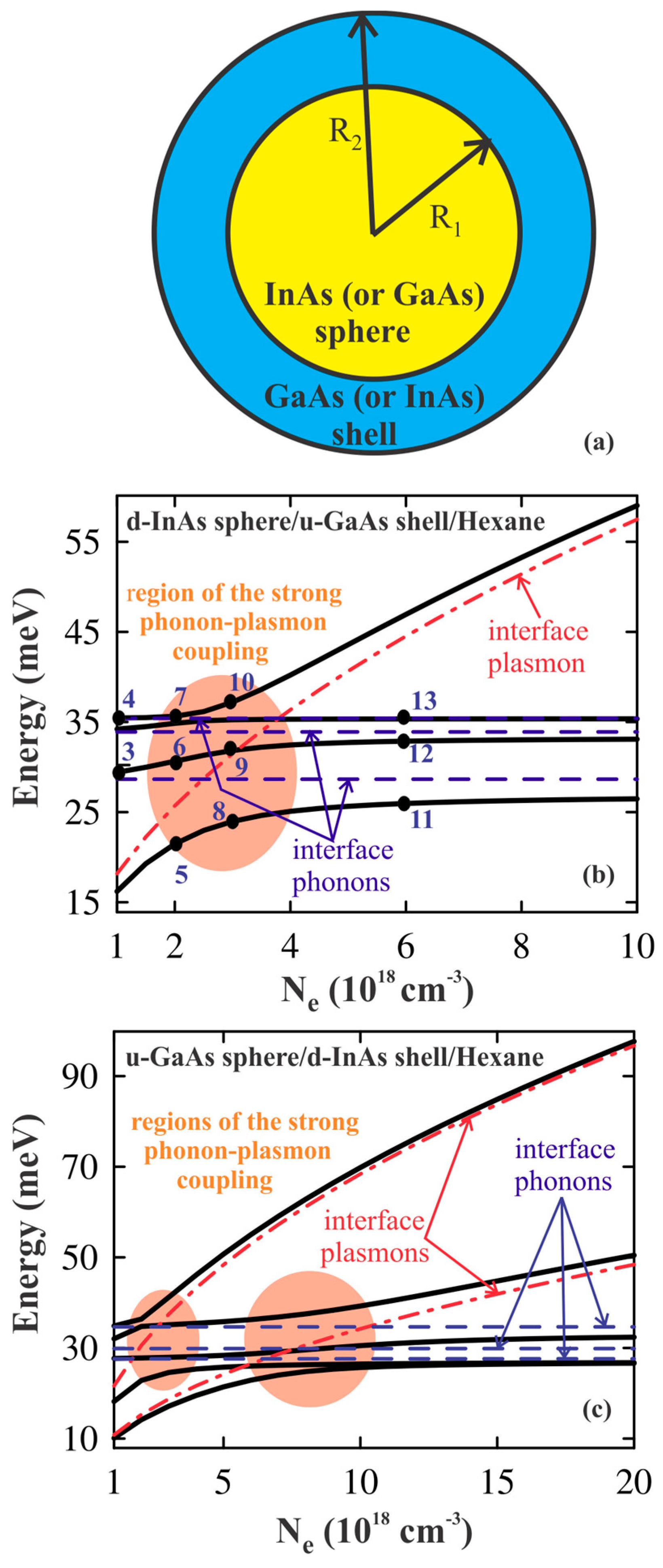
2. Phonons and Plasmons in Nanoshells

In order to describe the interface and surface phonons, and their coupling to the surface plasmons, the problem of finding the electrostatic potential in a planar multilayer structure needs to be addressed. This potential has been derived for an arbitrary number of layers in [48] (see also [49,50]). The method of [48] was later used to determine the electrostatic potential in multilayered spherical systems [51]. The phonon frequencies were obtained from the secular equation for the dynamical matrix [48,51].
There exist four types of phonon modes in spherical nanoshells: “sphere-like”, “shell-like”, “bulk-like”, and “interface” modes. The electrostatic potentials of sphere-like, shell-like, and bulk-like polar modes are confined to the core, shell, and outer regions, respectively, and do not penetrate the neighboring media. Due to their localization at interfaces, only the interface phonons strongly interact with the interface plasmons. The boundary conditions for the electrostatic potential of the polarization field follow from the continuity of the normal components of the electric displacement at the uncharged interfaces between the core and the shell, and between the shell and the outer region. The resulting boundary conditions,
b 11 V l ( R 1 ) + b 12 V l ( R 2 ) = 0 , b 21 V l ( R 1 ) + b 22 V l ( R 2 ) = 0
determine the frequencies and the amplitudes of the interface phonons (cf. [51]). In Equation (1), Rk is the radius of kth spherical layer (k = 1,2) and V l ( R k ) V ( R k , l , m ; ω ) is the amplitude of the polarization-induced electrostatic potential expanded in spherical harmonics with angular momentum quantum numbers l,m and frequency ω . In the remainder of this paper, the last two quantum numbers and the frequency are omitted. The coefficients b11, b12, b21, and b22 in Equation (1) are
b 11 = l R 1 ε 1 ( ω ) + ( R 1 R 2 ) l + 1 R 2 l R 2 l + 1 R 1 l R 1 l + 1 [ ( l + 1 ) ( R 2 R 1 ) l + l ( R 1 R 2 ) l + 1 ] ε 2 ( ω ) , b 12 = b 21 = ( 2 l + 1 ) R 1 l + 1 R 2 l + 1 / ( R 2 2 l + 1 R 1 2 l + 1 ) ε 2 ( ω ) , b 22 ( ω ) = ( R 1 R 2 ) l + 1 R 2 l R 2 l + 1 R 1 l R 1 l + 1 [ ( l + 1 ) ( R 1 R 2 ) l + l ( R 2 R 1 ) l + 1 ] ε 2 ( ω ) + ( l + 1 ) R 2 ε 3 ( ω ) ,
with the dielectric functions
ε i ( ω ) = { ε , i ( ω 2 ω L O , i 2 ω 2 ω T O , i 2 ω P l , i 2 ω 2 ) ,   if   the   i th   medium   is   doped ε , i ( ω 2 ω L O , i 2 ω 2 ω T O , i 2 ) ,   if   the   i th   medium   is   undoped   ( i = 1 , 2 ) ,
and
ε 3 ( ω ) = ε , 3 .
Equations (1) and (2) for the core/shell/outer medium nanostructures are a particular case of Equations (6) and (7) of [51], corresponding to the number of spherical layers K = 3 and the surface charge density σ = 0 . The efficient control over the yield and lifetime of a charge-separated state, by optimizing the shell thickness, allows for engineering core/shell nanostructures suitable for charge-transfer applications [52]. The appearance of interface charges, for instance, due to interactions with a biomolecule, leads to a detectable shift of the surface plasmon resonance frequency of the nanoshell [53]. In Equations (3) and (4), ε , i ( i = 1 , 2 , 3 ) is the optical dielectric constant of the ith medium, and ω L O , i and ω T O , i (i = 1, 2) are the frequencies of the LO and TO phonons in the ith medium, respectively. The bulk plasmon frequency in the ith medium is ω P l , i = e N e / ( m e , i ε , i ε 0 ) , where e is the absolute value of the electron charge, ε 0 is the vacuum dielectric permittivity, N e is the electron concentration, and m e , i is the electron band mass in the ith medium. We use, here, the Drude model of plasmons for InAs and GaAs, aiming at a general understanding of phonon–plasmon absorption spectra in semiconductor nanoshells. The multiband k × p method would be appropriate to obtain more precise predictions [54]. The dispersion equation for the hybrid interface phonon–plasmon eigenfrequencies is obtained from the secular equation for the set of algebraic equations (1):
b 11 b 22 b 12 2 = 0 .
The phonon–plasmon energies with quantum number l = 1 as a function of the electron concentration in the doped InAs are shown in Figure 1b,c for the d-InAs/u-GaAs/Hexane and the u-GaAs/d-InAs/Hexane nanoshells, respectively. Solid lines show the energies of the hybrid phonon–plasmon modes, calculated using Equation (5). Dashed and dash-dotted lines represent the energies of the non-interacting interface phonon and interface plasmon modes. These energies are obtained from Equation (5) by substituting ω P l , i = 0 into Equation (3) for the interface phonons and using ε I n A s ( ω ) = ε , I n A s ( 1 ω P l , I n A s 2 / ω 2 ) and ε G a A s ( ω ) = ε , G a A s for the interface plasmons. Here, ε , I n A s and ε , G a A s are the optical dielectric constants of InAs and GaAs, respectively. The interface plasmon and phonon modes are weakly coupled at both low electron concentrations (Ne < 1018 cm−3) and at high electron concentrations (Ne > 5 × 1018 cm−3 for the d-InAs/u-GaAs/Hexane nanoshell and Ne > 15 × 1018 cm−3 for the u-GaAs/d-InAs/Hexane nanoshell), and the energies of the interface polarization modes approach the limiting values for the non-interacting interface phonon and plasmon modes. The interface phonons and plasmons strongly interact and hybridize at intermediate electron concentrations, where these modes have comparable energies.

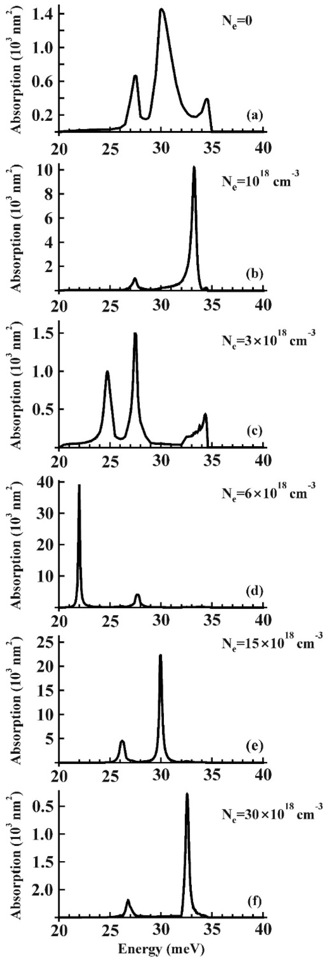
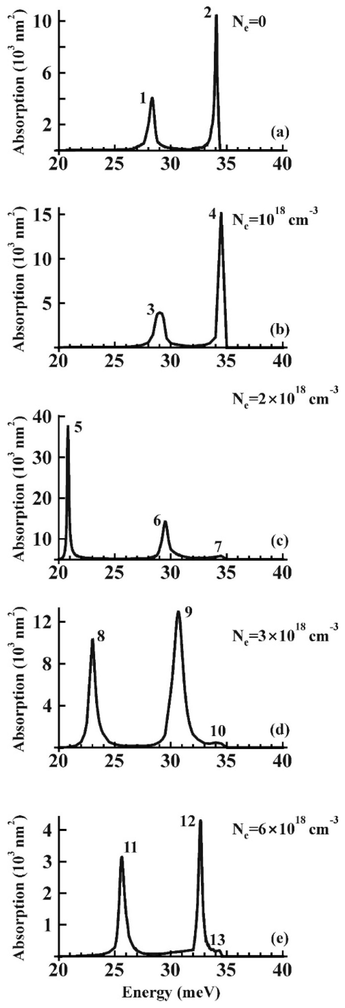
3. Results and Discussion

In the d-InAs/u-GaAs/Hexane nanostructure, there were four coupled phonon–plasmon branches (see Figure 1b) due to the hybridization of one interface plasmon branch (at the GaAs/InAs interface) and three interface phonon branches (InAs-like and GaAs-like at the InAs/GaAs interface and GaAs-like at the GaAs/Hexane interface). At around Ne ~ 3 × 1018 cm−3, the interface phonon–plasmon coupling was enhanced through the interaction with the single interface plasmon branch. In this nanostructure, it was the core that carried the doping, and only one interface between the core and the shell carried interface plasmons.
In the u-GaAs/d-InAs/Hexane nanostructure, three interface phonon branches (InAs-like and GaAs-like at the InAs/GaAs interface and InAs-like at the InAs/Hexane interface) hybridized with two interface plasmon branches at the GaAs/InAs and InAs/Hexane interfaces. This led to five coupled phonon–plasmon branches. As seen from Figure 1c, the interface phonon–plasmon hybridization in the u-GaAs/d-InAs/Hexane nanostructure was enhanced around Ne ~ 2 × 1018 cm−3 (due to the higher plasmon branch) and around Ne ~ 7 × 1018 cm−3 (due to the lower plasmon branch). Two interface plasmon branches were present because interface plasmons were excited at both interfaces (inner and outer) of the doped shell. Similar results have been obtained for quantum numbers l > 1.
The hybridized modes determined the absorption spectra of semiconductor nanoshells in the THz regime. Therefore, peaks in the absorption spectra can be used to identify hybrid phonon-plasmon modes. The peaks in the absorption spectrum can be identified with phonon–plasmon frequencies on the basis of Mie theory [26], extended to the case of concentric shells [55,56]. To apply this theory to the present case of semiconductor nanoshells, we used the following relative dielectric permittivities:
ε I n A s ( G a A s ) ( ω , N e ) = ε u n d o p e d I n A s ( G a A s ) ( ω ) ε , I n A s ( G a A s ) ω P l , b u l k 2 ( N e ) / ω 2 ,
where ε u n d o p e d I n A s ( G a A s ) ( ω ) is the relative dielectric function in undoped InAs (GaAs) tabulated from experiments [43]. For the calculation of the absorption spectrum, we used a complex dielectric function ε u n d o p e d I n A s ( G a A s ) ( ω ) , rather than the real function ε I n A s ( G a A s ) ( ω ) given by Equation (3).
Figure 2 and Figure 3 show the resulting absorption cross section as a function of the energy of the light impinging on the d-InAs/u-GaAs/Hexane and u-InAs/d-GaAs/Hexane core/shell nanostructures, respectively, for different doping levels of InAs. These nanostructures absorbed light in the energy range from 20 to 40 meV. The finite width of the absorption lines is due to the imaginary part of ε u n d o p e d I n A s ( G a A s ) ( ω ) . In the present paper, we focus on the light absorption by the core/shell nanostructures, and do not show the scattering cross section. In nanostructures with an undoped InAs core, the positions of the absorption peaks (indicated in Figure 2a as 1 and 2) correspond exactly to the energies of the nanoshell interface phonons at ω s , 1 = 28.5   meV , ω s , 2 = 33.8   meV , and ω s , 3 = 35.4   meV . The width of peak 2 is slightly larger than the difference between energies of the two highest interface phonons ω s , 3 ω s , 2 . Therefore, peak 2 was interpreted as the result of overlapping absorption peaks of the two highest interface phonon branches. An increase of the electron concentration to Ne = 1018 cm-3 (see Figure 2b) raised the spectral weight of the peaks by a factor of ~1.5 and weakly blue-shifts them (by approximately 1 meV). The peaks, indicated by filled circles with labels 3 and 4 in Figure 1b, correspond to light absorption by the three upper interface phonon–plasmon modes.
An additional increase of the electron concentration to Ne = 2 × 10¹⁸ and to 3 × 1018 cm−3 brought the system into the regime of enhanced phonon–plasmon interaction (marked in Figure 1b by a pink-shaded area). The resonant amplification of the absorption observed in this range of electron concentrations was due to the enhanced hybridization of interface phonon–plasmon modes. This led to an increase by a factor of ~3 of the low-energy absorption peak intensity for Ne = 2 × 1018 cm−3 (indicated with label 5 in Figure 2c) and by a factor of ~2 for Ne = 3 × 1018 cm−3 (indicated with label 8 in Figure 2d) as compared to the intensity of the peak labeled with 1 at Ne = 0 (see Figure 2a). The intensity of the absorption peaks labeled 6 and 9 remained nearly constant within the analyzed electron concentration range. A further increase of the electron concentration led to an attenuation of the interface phonon–plasmon interaction. The spectral weight of the absorption peaks decreased, and the peak positions shifted to the energies of the interface phonons (see Figure 2e).
The absorption spectrum of nanostructures with an undoped InAs shell shows three peaks (see Figure 3a), whose positions correspond to three interface phonon energies in the u-GaAs/u-InAs/Hexane nanoshell. Also, for this nanostructure, resonant amplification of the absorption took place for electron concentrations corresponding to enhanced interface phonon–plasmon interaction (shown in Figure 1c by pink-shaded areas). The first resonance near Ne = 1018 cm−3 (see Figure 3b) is characterized by an increase of the intensity of the absorption peak near 33 meV with a factor of ~8. This increase resulted from the interaction of interface phonons with interface plasmons in the upper plasmon branch. As before, we find that an increase of the electron concentration from Ne = 1018 cm−3 to Ne = 3 × 1018 cm−3 led to a weakening of the absorption. The spectral weight became approximately the same as that for Ne = 0 (see Figure 3c). In the electron concentration range from Ne = 5 × 10¹⁸ to 15 × 1018 cm−3, there was a second resonant amplification of the absorption, now associated with the hybridization of the interface phonons with the plasmons from the lower interface plasmon branch. In this case, the nanostructure efficiently absorbed light in a broad electron concentration range from 5 × 10¹⁸ to 15 × 1018 cm−3 (see Figure 3d,e). At higher electron concentrations, light absorption in the nanostructure was significantly reduced. A strong phonon–plasmon coupling and a resonant amplification of the absorption can also be realized in doped semiconductor quantum dots of different materials and shapes, including InAs/GaAs core/shell quantum dots grown on Si substrate [57], colloidal CdSe/CdS and CdSe/ZnS quantum dots [58], or semiconductor quantum dots without a shell [31,59,60]. However, core/shell nanocrystals allow for better control over the absorption spectrum through the selection of the core/shell thickness ratio and the material of the shell.

4. Conclusions

We have theoretically investigated hybrid interface phonon–plasmon modes and the resulting light absorption in d-InAs/u-GaAs/Hexane and u-GaAs/d-InAs/Hexane nanoshells. By varying the electron concentration in InAs, the strength of the interface phonon–plasmon interaction can be adjusted, leading to a resonant increase of the light absorption by a factor of 3 to 4. The u-GaAs/d-InAs/Hexane nanoshell resonantly absorbs light in a broader range of electron concentrations than the d-InAs/u-GaAs/Hexane nanoshell. The difference between the light absorption spectra for these structures is explained by the presence of two interface plasmon branches in the u-GaAs/d-InAs/Hexane nanoshell, whereas the other structure had only one branch. This offers interesting perspectives for realizing doping-dependent resonances in the THz response of semiconductor nanoshells.

Author Contributions

Conceptualization, all authors; investigation, D.L.N., E.P.P. and V.M.F; writing—original draft preparation, all authors; writing—review and editing, D.L.N. and V.M.F.

Funding

This research was funded by the Fund for Scientific Research—Flanders, FWO grant G.0365.08; by the WOG WO.033.09N—Belgium; by the Government of the Republic of Moldova, grant 15.817.02.29F and by the German Research Foundation (DFG, Germany), grant number FO 956/4-1 and FO 956/5-1.

Acknowledgments

The authors thank M. Benyoucef, V. N. Gladilin, S. N. Klimin and G. P. Papari for valuable discussions.

Conflicts of Interest

The authors declare no conflict of interest.

References

  1. Sothmann, B.R.; Sánchez, R.; Jordan, A.N.; Büttiker, M. Powerful energy harvester based on resonant-tunneling quantum wells. New J. Phys. 2013, 15, 095021. [Google Scholar] [CrossRef] [Green Version]
  2. Xia, Y.; Yang, P.; Sun, Y.; Wu, Y.; Mayers, B.; Gates, B.; Yin, Y.; Kim, F.; Yan, H. One-Dimensional Nanostructures: Synthesis, Characterization, and Applications. Adv. Matter. 2003, 15, 353–389. [Google Scholar] [CrossRef]
  3. Corfdir, P.; Marquardt, O.; Lewis, R.B.; Sinito, C.; Ramsteiner, M.; Trampert, A.; Jahn, U.; Geelhaar, L.; Brandt, O.; Fomin, V.M. Excitonic Aharonov–Bohm Oscillations in Core–Shell Nanowires. Adv. Mater. 2019, 31, 1805645. [Google Scholar] [CrossRef] [PubMed]
  4. Nika, D.L.; Balandin, A.A. Phonons and thermal transport in graphene and graphene-based materials. Rep. Prog. Phys. 2017, 80, 036502. [Google Scholar] [PubMed] [Green Version]
  5. Renteria, J.D.; Nika, D.L.; Balandin, A.A. Graphene thermal properties: Applications in thermal management and energy storage. Appl. Sci. 2014, 4, 525–547. [Google Scholar] [CrossRef]
  6. Cocemasov, A.I.; Isacova, C.I.; Nika, D.L. Thermal transport in semiconductor nanostructures, graphene, and related two-dimensional materials. Chin. Phys. B 2018, 27, 056301. [Google Scholar] [CrossRef] [Green Version]
  7. Deneke, C.; Songmuang, R.; Jin-Phillipp, N.Y.; Schmidt, O.G. The structure of hybrid radial superlattices. J. Phys. D Appl. Phys. 2009, 42, 103001. [Google Scholar] [CrossRef]
  8. Fomin, V.M.; Balandin, A.A. Phonon Spectrum Engineering in Rolled-up Micro- and Nano-Architectures. Appl. Sci. 2015, 5, 728–746. [Google Scholar] [Green Version]
  9. Li, G.; Yarali, M.; Cocemasov, A.; Baunack, S.; Nika, D.L.; Fomin, V.M.; Singh, S.; Gemming, T.; Zhu, F.; Mavrokefalos, A.; et al. In-plane thermal conductivity of radial and planar Si/SiOx hybrid nanomembrane superlattices. ACS Nano 2017, 11, 8215–8222. [Google Scholar] [CrossRef] [PubMed]
  10. Fomin, V.M. (Ed.) Physics of Quantum Rings, 2nd ed.; Springer International Publishing: Cham, Switzerland, 2018; 596p. [Google Scholar]
  11. Bimberg, D. (Ed.) Semiconductor Nanostructures; Springer: Berlin/Heidelberg, Germany, 2008; 357p. [Google Scholar]
  12. Chen, Y.; Zopf, M.; Keil, R.; Ding, F.; Schmidt, O.G. Highly-efficient extraction of entangled photons from quantum dots using a broadband optical antenna. Nat. Commun. 2018, 9, 2994. [Google Scholar] [CrossRef] [PubMed]
  13. Daniel, M.-C.; Astruc, D. Gold Nanoparticles:  Assembly, Supramolecular Chemistry, Quantum-Size-Related Properties, and Applications toward Biology, Catalysis, and Nanotechnology. Chem. Rev. 2004, 104, 293–346. [Google Scholar] [CrossRef] [PubMed]
  14. Myroshnychenko, V.; Rodríguez-Fernández, J.; Pastoriza-Santos, I.; Funston, A.M.; Novo, C.; Mulvaney, P.; Liz-Marzán, L.M.; García de Abajo, F.J. Modeling the optical response of gold nanoparticles. Chem. Soc. Rev. 2008, 37, 1792–1805. [Google Scholar] [CrossRef] [PubMed]
  15. Bardhant, R.; Grady, N.K.; Ali, T.; Halas, N.J. Metallic nanoshells with semiconductor cores: Optical characteristics modified by core medium properties. ACS Nano 2010, 4, 6169–6179. [Google Scholar] [CrossRef]
  16. Chen, X.; Fang, J.; Zhang, X.D.; Zhao, Y.; Gu, M. Optical/electrical integrated design of core–shell aluminum-based plasmonic nanostructures for record-breaking efficiency enhancements in photovoltaic devices. ACS Photonics 2017, 4, 2102–2110. [Google Scholar] [CrossRef]
  17. Choi, C.K.K.; Zhuo, X.L.; Chiu, Y.T.E.; Yang, H.R.; Wang, J.F.; Choi, C.H.J. Polydopamine-based concentric nanoshells with programmable architectures and plasmonic properties. Nanoscale 2017, 9, 16968–16980. [Google Scholar] [CrossRef] [PubMed]
  18. Yang, T.; Guo, K.; Liu, G.; Yang, Y.; Li, K.; Zhai, W. Enhancement of surface plasmon resonances on nonlinear optical properties in spherical dome semiconductor nanoshells. Superlattice Microstruct. 2018, 122, 394–403. [Google Scholar] [CrossRef]
  19. Ktatami, M.; Alijani, H.Q.; Nejad, M.S.; Varma, R.S. Core@shell Nanoparticles: Greener Synthesis Using Natural Plant Products. Appl. Sci. 2018, 8, 411. [Google Scholar] [CrossRef]
  20. Averitt, R.D.; Sarkar, D.; Halas, N.J. Plasmon resonance shifts of au-coated Au2S nanoshells: Insight into multicomponent nanoparticle growth. Phys. Rev. Lett. 1997, 78, 4217. [Google Scholar] [CrossRef]
  21. Oldenburg, S.J.; Averitt, R.D.; Westcott, S.L.; Halas, N.J. Nanoengineering of optical resonances. Chem. Phys. Lett. 1998, 288, 243–247. [Google Scholar] [CrossRef]
  22. Prodan, E.; Nordlander, P. Exchange and correlations effects in small metallic nanoshells. Chem. Phys. Lett. 2001, 349, 153–160. [Google Scholar] [CrossRef]
  23. Prodan, E.; Nordlander, P. Electronic structure and polarizability of metallic nanoshells. Chem. Phys. Lett. 2002, 352, 140–146. [Google Scholar] [CrossRef]
  24. Prodan, E.; Lee, A.; Nordlander, P. The effect of a dielectric core and embedding medium on the polarizability of metallic nanoshells. Chem. Phys. Lett. 2002, 360, 325–332. [Google Scholar] [CrossRef]
  25. Amendola, V.; Pilot, R.; Frasconi, M.; Marago, O.M.; Iati, M.A. Surface plasmon resonance in gold nanoparticles:a review. J. Phys. Cond. Matt. 2017, 29, 203002. [Google Scholar] [CrossRef]
  26. Mie, G. Beiträge zur Optik trüber Medien, speziell kolloidaler Metallösungen. Ann. Physik 1908, 25, 377–445. [Google Scholar] [CrossRef]
  27. Karker, N.A.; Carpenter, M.A. High figure of merit hydrogen sensor using multipolar plasmon resonance modes. Sens. Actuators B 2017, 252, 385–390. [Google Scholar] [CrossRef]
  28. Esmaeilzadeh, H.; Rivard, M.; Arzi, E.; Légaré, F.; Hassani, A. Smart textile plasmonic fiber dew sensors. Opt. Express 2015, 23, 14981–14992. [Google Scholar] [CrossRef]
  29. Li, J.F.; Zhang, Y.J.; Ding, S.Y.; Panneerselvam, R.; Tian, Z.Q. Core–Shell Nanoparticle-Enhanced Raman Spectroscopy. Chem. Rev. 2017, 117, 5002–5069. [Google Scholar] [CrossRef]
  30. Agrawat, A.; Cho, S.H.; Zandi, O.; Ghosh, S.; Johns, R.W.; Milliron, D.J. Localized Surface Plasmon Resonance in Semiconductor Nanocrystals. Chem. Rev. 2018, 118, 3121–3207. [Google Scholar] [CrossRef]
  31. Lee, J.D. Optical absorption of semiconducting and metallic nanospheres with the confined electron-phonon coupling. J. Chem Phys. 2006, 124, 194706. [Google Scholar] [CrossRef]
  32. Santavicca, D.F.; Reulet, B.; Karasik, B.S.; Pereverzev, S.V.; Olaya, D.; Gershenson, M.E.; Frunzio, L.; Prober, D.E. Energy resolution of terahertz single-photon-sensitive bolometric detectors. Appl. Phys. Lett. 2010, 96, 083505. [Google Scholar] [CrossRef] [Green Version]
  33. Ryzhii, V.; Ryzhii, M.; Mitin, V.; Otsuji, T. Terahertz and infrared photodetection using p-i-n multiple-graphene-layer structures. J. Appl. Phys. 2010, 107, 054512. [Google Scholar] [CrossRef] [Green Version]
  34. Marinchio, H.; Chusseau, L.; Torres, J.; Nouvel, P.; Varani, L.; Sabatini, G.; Palermo, C.; Shiktorov, P.; Starikov, E.; Gružinskis, V. Room-temperature terahertz mixer based on the simultaneous electronic and optical excitations of plasma waves in a field effect transistor. Appl. Phys. Lett. 2010, 96, 013502. [Google Scholar] [CrossRef]
  35. Zheludev, N.I.; Kivshar, Y.S. From metamaterials to metadevices. Nat. Mater. 2012, 11, 917. [Google Scholar] [CrossRef]
  36. Foteinopoulou, S.; Kafesaki, M.; Economou, E.N.; Soukoulis, C.M. Two-dimensional polaritonic photonic crystals as terahertz uniaxial metamaterials. Phys. Rev. B 2012, 84, 035128. [Google Scholar] [CrossRef]
  37. Sugunan, A.; Zhao, Y.; Mitra, S.; Dong, L.; Li, S.; Popov, S.; Marcinkevicius, S.; Toprak, M.S.; Muhammed, M. Synthesis of tetrahedral quasi-type-II CdSe–CdS core–shell quantum dots. Nanotechnology 2011, 22, 425202. [Google Scholar] [CrossRef]
  38. Clark, S.W.; Harbold, J.M.; Wise, F.W. Resonant energy transfer in PbS quantum dots. J. Phys. Chem. 2007, 111, 7302–7305. [Google Scholar] [CrossRef]
  39. Yang, H.-J.; Tuan, H.-Y. Efficient and scalable synthesis of quantum dots using hexane as the solvent in a non-microfluidic flow reactor system. RSC Adv. 2014, 4, 51926–51934. [Google Scholar] [CrossRef]
  40. Material parameters of InAs and GaAs. Available online: http://www.ioffe.ru/SVA/NSM/Semicond/ (accessed on 2 April 2019).
  41. Vurgaftman, I.; Meyer, J.R. Band parameters for III–V compound semiconductors and their alloys. J. Appl. Phys. 2001, 89, 5815–5875. [Google Scholar] [CrossRef]
  42. Schooss, D.; Mews, A.; Eychmuller, A.; Weller, H. Quantum-dot quantum well CdS/HgS/CdS: Theory and experiment. Phys. Rev. B 1994, 49, 17072. [Google Scholar] [CrossRef]
  43. Adachi, S. Optical Constants of Crystalline and Amorphous Semiconductor: Numerical Data and Graphical Information; Kluwer Academic Publishers: Boston, MA, USA, 2004; 714p. [Google Scholar]
  44. Schaller, R.D.; Pietryga, J.M.; Klimov, V.I. Carrier Multiplication in InAs Nanocrystal Quantum Dots with an Onset Defined by the Energy Conservation Limit. Nano Lett. 2007, 7, 3469. [Google Scholar] [CrossRef]
  45. Lim, H.; Zhang, W.; Tsao, S.; Sills, T.; Szafraniec, J.; Mi, K.; Movaghar, B.; Razeghi, M. Quantum dot infrared photodetectors: Comparison of experiment and theory. Phys. Rev. B 2005, 72, 085332. [Google Scholar] [CrossRef]
  46. Makeev, M.A. Self-Organized Quantum Dot Superstructures for Nanoelectronic and Optoelectronic Applications. J. Nanoelectron. Optoelectron. 2006, 1, 176. [Google Scholar] [CrossRef]
  47. Sargent, E.H. Colloidal quantum dot solar cells. Nat. Photonics 2012, 6, 133. [Google Scholar] [CrossRef]
  48. Fomin, V.M.; Pokatilov, E.P. Optical Properties of Multi-Layer Structures. IV. Non-Linear Absorption of light in Multi-Layer Structures. Phys. Stat. Sol. B 1993, 176, 355. [Google Scholar] [CrossRef]
  49. Ridley, B.K. Electrons and Phonons in Semiconductor Multilayers; Cambridge University Press: Cambridge, UK, 1997; 330p. [Google Scholar]
  50. Stroscio, M.A.; Dutta, M. Phonons in Nanostructures; Cambridge University Press: Cambridge, UK, 2001; 274p. [Google Scholar]
  51. Klimin, S.N.; Pokatilov, E.P.; Fomin, V.M. Bulk and interface polarons in quantum wires and dots. Phys. Stat. Sol. B 1994, 184, 373. [Google Scholar] [CrossRef]
  52. Zhu, H.; Song, N.; Lian, T. Wave function engineering for ultrafast charge separation and slow charge recombination in type II core/shell quantum dots. J. Am. Chem. Soc. 2011, 133, 8762. [Google Scholar] [CrossRef]
  53. Predeep, T. Nano: The Essentials. Understanding of Nanoscience and Nanotechnology; McGraw-Hill: New Delhi, NY, USA, 2007; 267p. [Google Scholar]
  54. Vukmirović, N.; Gačević, Ž; Ikonić, Z.; Indjin, D.; Harrison, P.; Milanović, V. Intraband absorption in InAs/GaAs quantum dot infrared photodetectors—Effective mass versus k × p modelling. Semicond. Sci. Technol. 2006, 21, 1098–1104. [Google Scholar]
  55. Aden, A.L.; Kerker, M. Scattering of electromagnetic waves from two concentric spheres. J. Appl. Phys. 1951, 22, 1242–1246. [Google Scholar] [CrossRef]
  56. Tzarouchis, D.; Sihvola, A. Light scattering by a dielectric sphere: Perspectives on the Mie resonances. Appl. Sci. 2018, 8, 184. [Google Scholar] [CrossRef]
  57. Reithmaier, J.P.; Benyoucef, M. III-V on Silicon nanocomposites. In Semiconductors and Semimetals; Lourdudoss, S., Chen, R., Jagadish, C., Eds.; Academic Press: Cambridge, MA, USA, 2018; Volume 2, pp. 27–42. [Google Scholar]
  58. Jing, P.; Zheng, J.; Zeng, Q.; Zhang, Y.; Liu, X.; Liu, X.; Kong, X.; Zhao, J.J. Shell-dependent electroluminescence from colloidal CdSe quantum dots in multilayer light-emitting diodes. Appl. Phys. 2009, 105, 044313. [Google Scholar] [CrossRef]
  59. Lalayan, A.; Avetisyan, A.; Djotyan, A. The luminescence properties of the colloidal GaAs and CdS semiconductor quantum dots. Laser Phys. Lett. 2005, 2, 12–15. [Google Scholar] [CrossRef]
  60. Liu, Z.; Liu, C.; Li, Q.; Chen, Z.; Gong, Q. Preparation, characterization and nonlinear optical properties of colloidal gallium arsenide nanocrystals. Rare Metals 2006, 25, 118–123. [Google Scholar] [CrossRef]
Figure 1. A scheme of the spherical core/shell/outer medium nanostructure (a). Full curves show the interface phonon–plasmon energies versus the electron concentration in the d-InAs/u-GaAs/Hexane nanostructure and (b) u-GaAs/d-InAs/Hexane nanostructure (c). Dashed and dash-dotted curves represent the limiting cases, as discussed in the text. Full circles, labeled by numbers, indicate energies corresponding to the absorption peaks shown in Figure 2. The radii of the circles represent the calculation error. The pink-shaded areas indicate the regions of strong interface phonon-plasmon hybridization.
Applsci 09 01442 g001
Figure 2. Light absorption cross section versus the photon energy for the d-InAs/u-GaAs/Hexane nanostructure. The numbers used as peak labels correspond to the interface phonon-plasmon modes in Figure 1b.
Applsci 09 01442 g002
Figure 3. Light absorption cross section versus the photon energy for the u-GaAs/d-InAs/Hexane nanostructure.
Applsci 09 01442 g003

