1. Introduction
In spite of recent developments in new photovoltic technologies and decreases in the cost of mature ones [
1,
2,
3,
4], dye-sensitised solar cells (DSCs) are still of interest to both researchers and industry. This is at least in part due to their application in large-scale built-in photovoltaics (BIPV) as power windows, due to features such as transparency and the range of dye colours which may be employed. Additionaly, DSCs are expected to find significant use in indoor applications in the near future, for which efficiencies over 28% using artificial lighting have already been reported [
5], where the DSC absorption spectra was tuned to better match the light source used. DSCs also have a benefit in that they are not significantly affected by partial shading, changes in temperature or the light incident angle, as silicon solar cells tend to be [
5,
6,
7,
8].
TiO
2 photoanodes can be fabricated with different degrees of transparency, depending on the particle size and the paste preparation process [
9,
10]. Well-dispersed, small particles can result in a high transmission photoanode (>80%) across the visible range [
11]. On the other hand, light scattering is a widely employed technique to increase the mean pathlength of photons through the photoanode, leading to an increased likelihood of said photons being absorbed by bound dyes [
11,
12,
13]. This is particularly pertinent when the extinction co-efficient of the dye is low, and simply making the photoanode film thicker leads to increased charge recombination. Indeed, many researchers have intentionally tuned the light scattering properties of their particles to enhance the light-harvesting efficiency (LHE) [
10,
14,
15,
16]. However, this is less necessary because of recent developments in sensitiser design and is not desirable for most BIPV applications.
A large portion of work published on DSC development (~40%, which equates to more than 1200 publications) has been on the synthesis and/or modification of metal oxides, mostly TiO
2, as efficient photoanode materials [
17]. The vast majority of synthesised TiO
2 nanoparticles in these reports were dried, calcined and then re-dispersed to make a printable paste [
14,
18,
19]. While a handful of exceptions exists where the nanoparticles were kept in suspension after their synthesis [
7,
10,
11], producing a transparent film due to the high nanoparticle dispersion.
In 2008 Ito et al. reported high-efficiency DSC based on TiO
2 nanoparticles, with solvent transfer from the synthetic medium to the screen-printing paste matrix, where the TiO
2 was sensitised with the ruthenium complex N719. In this case, both small particle (transparent) and a second layer of larger, scattering particles were employed, as well as an anti-reflective film. The optimum thickness of a bi-layer photoanode including a transparent layer and a large scattering layer was 12–14 μm, and photovoltaic conversion efficiencies (PCEs) of 9.1% and 10% were reported for the transparent photoanode- and bi-layer (scattering) photoanode-based devices, respectively [
10]. A few years later, Yoon et al. investigated the effect of photoanode transparency and thickness on DSC performance for BIPV application. Using a protocol without drying their nanoparticles, they were able to obtain a printable paste and then deposit a transparent photoanode, which was subsequently sensitised with N719. Their best PCEs were 5.13% and 6.64% for photoanode thicknesses 8.13 μm and 32.2 μm, respectively [
7]. More recently, Sanchez et al. provided further insight as they studied the effect of autoclave pressure in hydrothermal synthesis on the pore and particle sizes of non-scattering TiO
2 photoanodes, again sensitised with the N719 dye, with an optimized PCE of 5.63% [
20].
Until recently, the organometallic dye N719 has been a staple of DSC research, in spite of high production costs and the low extinction coefficient [
21]. Metal-free organic dyes have attracted attention, including application in record PCE devices [
21,
22,
23]. The indole-based metal-free dye D149 is one of the most widely reported organic dyes and is commercially available [
24,
25].
There is, to our knowledge, only one report comparing the two paste-making approaches, and while this article makes direct comparisons regarding the photoanode transparency, it does not look at the solar cell performance of the devices with photoanodes made with the same material but through different processes [
11]. In 2017, Zama et al. used a wet-acid method and rotary evaporation to obtain the paste directly from a nanoparticle suspension after thermal treatment by adding organic binders and solvents in suitable ratios. They produced another paste in a similar way but included a drying step. They discussed the effect of using two paste preparation approaches on the transparency and surface morphology of TiO
2 photoanode; however, there was no direct comparison of the performance of DSCs using these two approaches. They did, however, report a PCE of 5.2%, compared to that of 4.63% obtained when using NR18-T [
11].
In this work, we make a direct comparison between these two paste-making approaches, in terms of both optical properties and subsequent photovoltaic properties. We do this with solvothermally-synthesised anatase nanoparticles, labelled SANP-S and SANP-T depending on the presence or absence of a drying step, respectively. We also compare the use of N719 and D149 as dyes in this study, as the higher extinction co-efficient of the organic dye is expected to mitigate the importance of the scattering effects. We recently reported on this TiO
2 material (SANP) and its performance in efficient DSCs, showing that it benefited from a high isoelectric point (IEP) which led to increased dye loading [
26].
2. Results and Discussion
SANP-S was synthesised by a new and facile one-step solvothermal process, as reported elsewhere [
26]. Briefly, titanium isopropoxide (TTIP, Sigma, USA) (1.5 mL) was added dropwise to an acetic acid (Sigma, USA)–ethanol (Chem-Supply, Australia) mixed solvent (1:2 v/v) under vigorous stirring for (1 h) at room temperature. A transparent solution was formed, which was then transferred into a 45 mL Teflon-lined stainless steel autoclave (Parr Instrument Company, USA) and heated to 200 °C (ramp time of 1 °C /min) for 9 h. After cooling down to room temperature, the resulting white precipitate was collected and washed with distilled water and ethanol three times. The material for SANP-S was then dried overnight at 90 °C and calcined at 500 °C (ramp time of 1 °C /min) in the air for three hours. This was then redispersed in ethanol, while SANP-T was maintained in ethanol. The dispersions were combined with terpineol (Alfa Aesar, USA) and ethyl cellulose (Sigma, USA) to create pastes similar to those in our previous reports [
15,
18,
27]. These pastes were then screen-printed onto substrates and calcined following a multi-step program up to 500 °C.
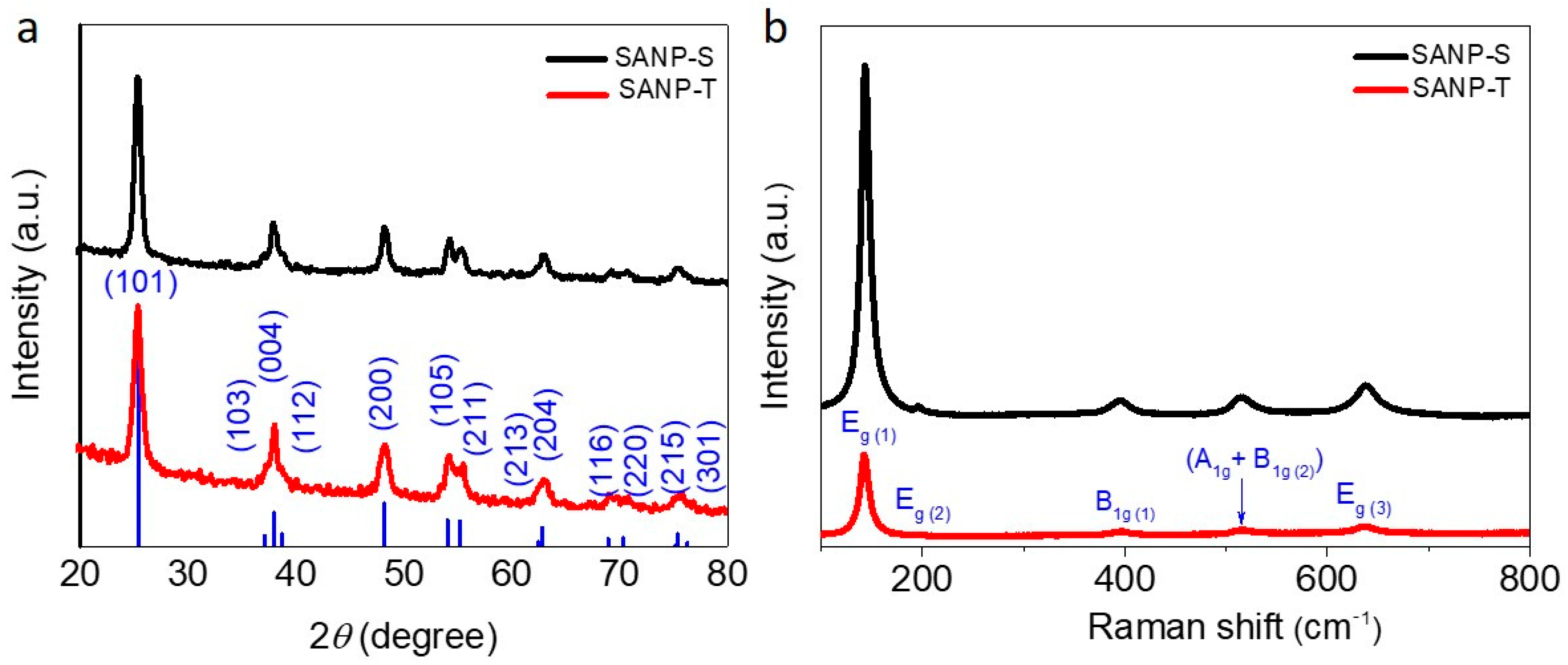
The X-ray diffraction (XRD) patterns in
Figure 1a show that the samples collected from printed films of SANP-S and SANP-T were both phase-pure and well-crystallised anatase TiO
2 (JSPD.21-1272), with crystalite sizes of around 25 nm. The SANP-S sample showed slightly narrower peaks, implying slightly higher crystallinity due to the additional sintering time. Previously, we demonstrated the role amorphous content plays on DSC performance, as a result of decreased charge injection efficiency [
18]. Preliminary measurements showed the amorphous content to be quite low in these materials (only a few percent at most; data to be published elsewhere [
26]), indicating that this would not be a major factor affecting the charge injection efficiency. Raman spectra of SANP-S and SANP-T (
Figure 1b) also showed both materials to be anatase TiO
2, confirmed by six characteristic Raman vibrational modes centered at 144 cm
−1 (E
g (1)), 197 cm
−1 (E
g (2)), 399 cm
−1 (B
1g), 513 cm
−1 (A
1g), 519 cm
−1 (B
1g), and 639 cm
−1 (E
g (3)), respectively [
28]. The slightly higher intensity (less broadening) of peaks in SANP-S again indicates better crystallinity compared to SANP-T.
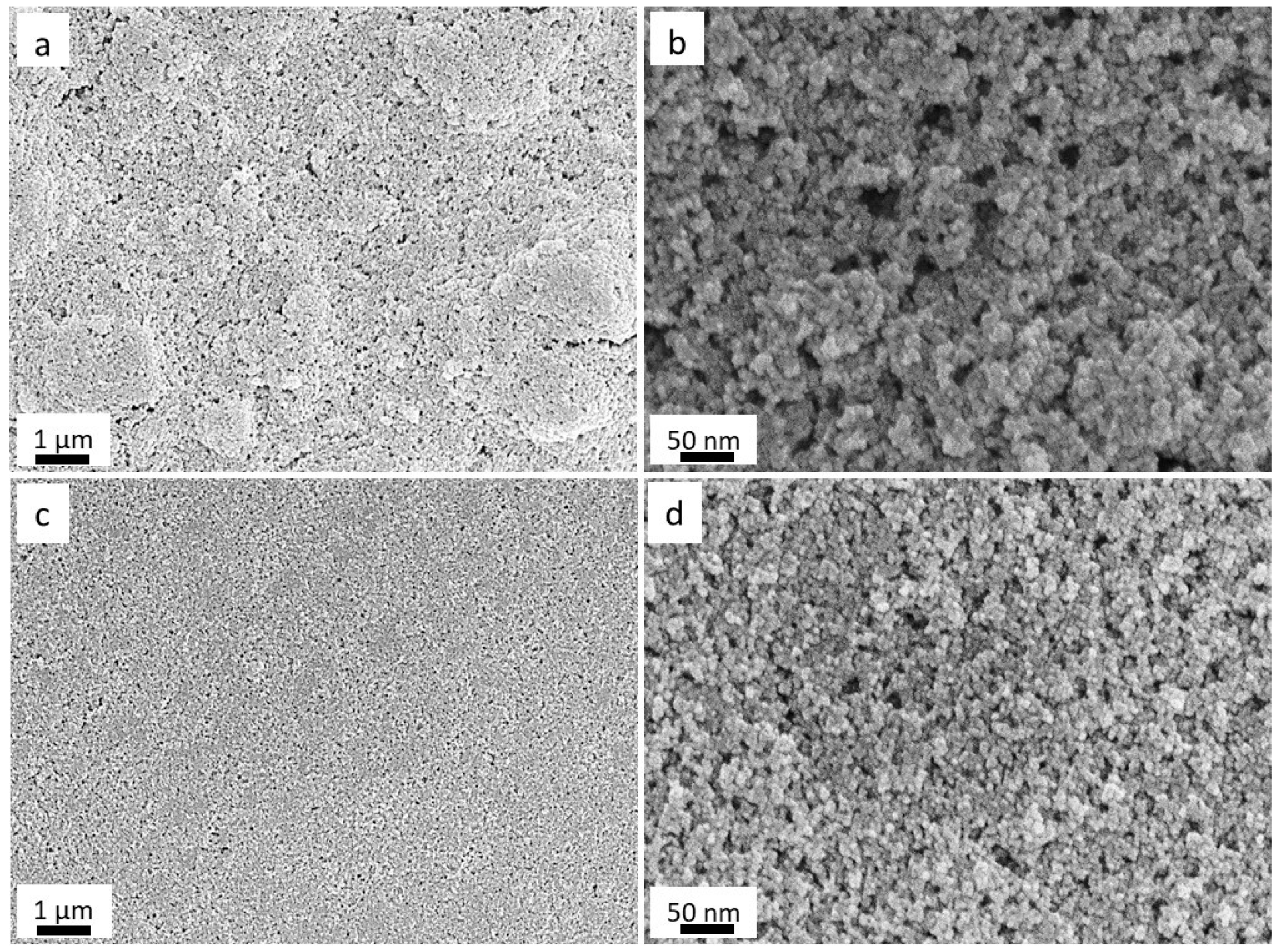
The low- and high-magnification scanning electron microscope (SEM) images (
Figure 2a–d) show the morphologies of SANP-S and SANP-T films. It can be observed that SANP-S (
Figure 2a,b) had a more aggregated structure and non-uniform surface topography compared to SANP-T (
Figure 2c,d), in line with our expectations. SANP-S films also showed significant cracking at this scale, which is attributed to aggregation. Both had similar particle size about 25 ± 3 nm, in line with the above XRD results.
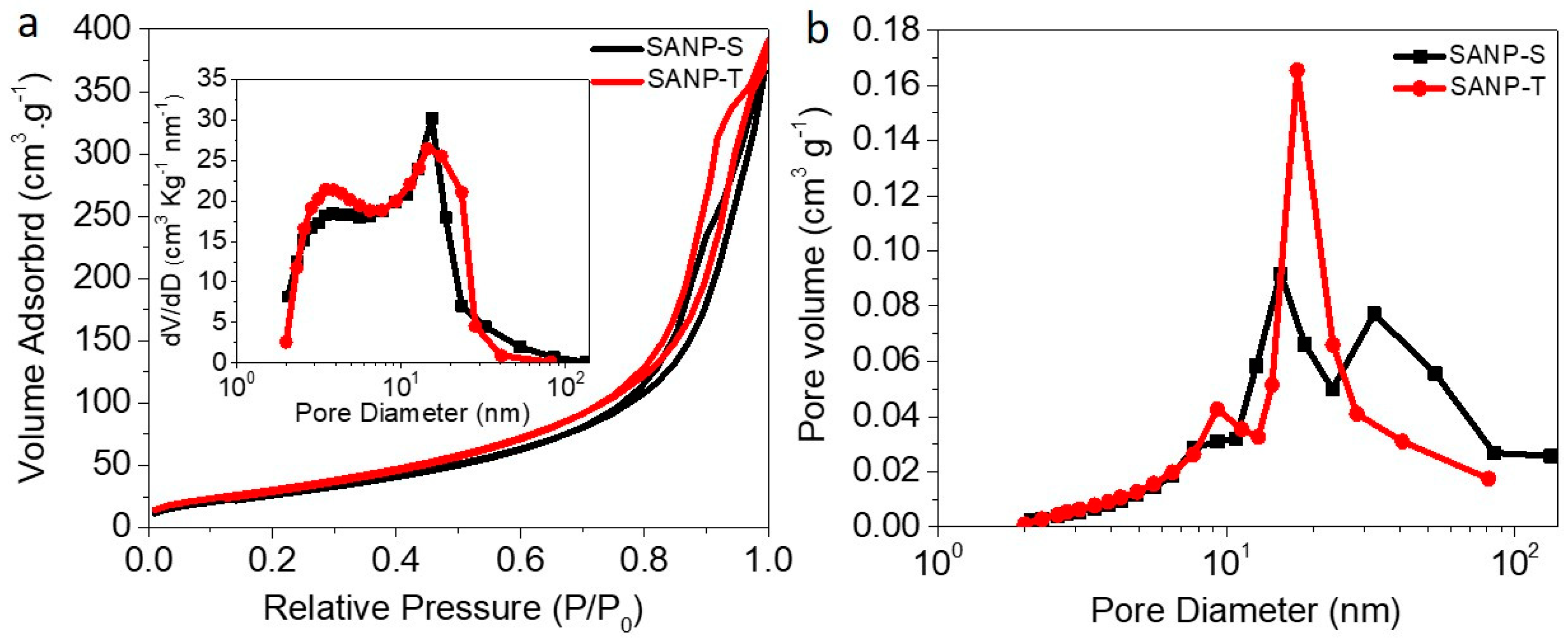
Figure 3a,b show the specific surface area and the pore size distributions in the two structures. The type (IV) nitrogen adsorption/desorption isotherm branches indicate that both materials have mesoporous structure [
29,
30] with similar porosities of ~64% (
Figure 3a). [
27] On the other hand, SANP-T has a more uniform pore size distribution, with a broader range of pores in the 2–30 nm range. SANP-S also revealed some larger pores, as shown in
Figure 3b, which were attributed to the cracked structure seen in SEM images above and in (
Figure S1, Supplementary Materials). The SANP-S also has a slightly lower surface area (113 m
2·g
−1) compared to SANP-T (119 m
2·g
−1), which could be attributed to aggregation, and is in line with our previous experimental results for similar systems [
15].
2.1. Optical Properties of Printed SANP-S and SANP-T Films
Since both dye loading and light scattering affect the LHE, these properties were quantified for SANP-S and SANP-T films, including dye loading after sensitisation with either D149 or N719 [
31].
Figure 4a,b (and
Table 1) show the results of the dye desorption experiments, with SANP-T films hosting slightly more dye compared to SANP-S films of the same thickness. This is roughly in line with the differences in surface area reported above. Meanwhile, undyed SANP-S films (10 μm) showed a considerably higher diffuse reflection (35–55%) (with lower direct transmittance) than undyed SANP-T (5–10%), as shown in
Figure 4c and (
Figure S2, Supplementary Materials) and in the visual images of photoanode films (
Figure 5).
2.2. Solar Performance of SANP-S and SANP-T Devices
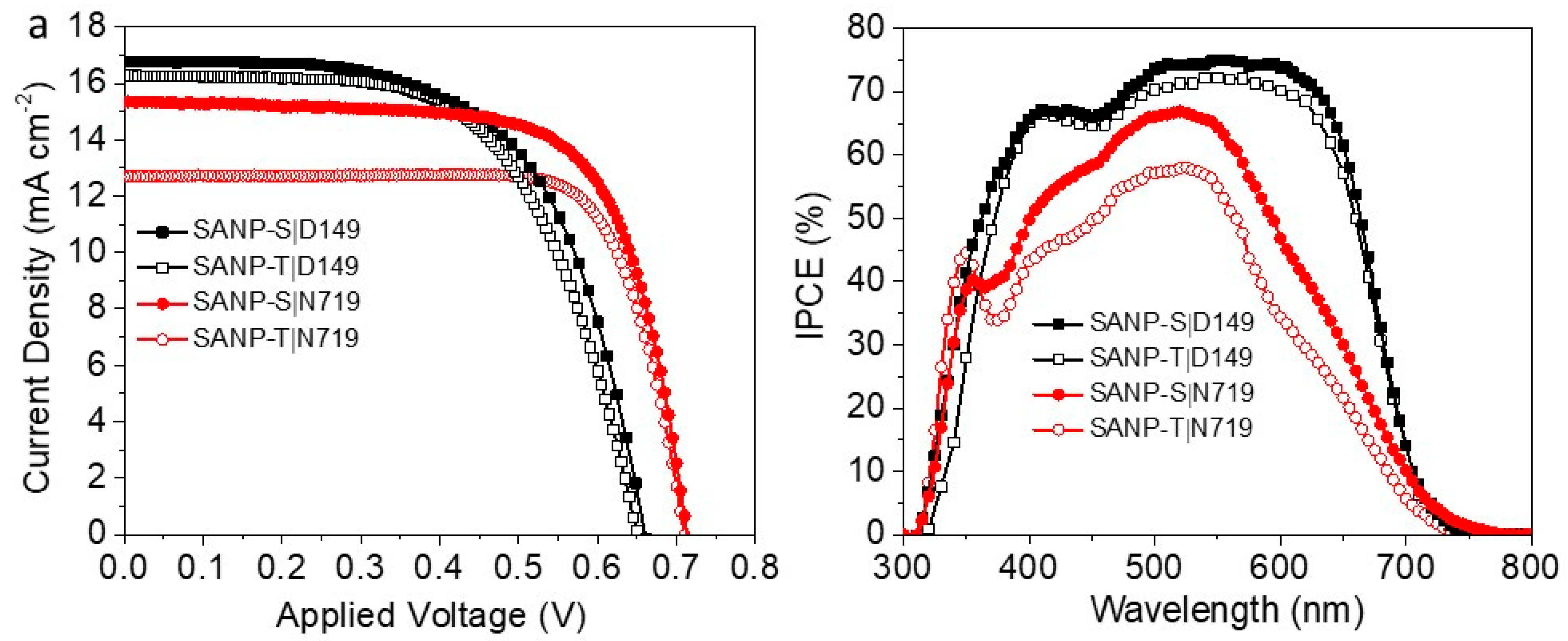
The photovoltaic performances of DSCs based on SANP photoanodes (10.0 ± 0.5 µm) were compared, with the current–voltage responses (J–V) and incident photon to charge carrier efficiency (IPCE) results shown in
Figure 6a,b and (
Figure S3, highlighted scattering effects on IPCE responses,
Supplementary Materials) and
Table 2 and (
Table S1, Supplementary Materials). In brief, devices based on SANP-S were more efficient than those using SANP-T films. The differences were more significant with the lower absorbing N719 (peak ε ~ 14700 M
−1·cm
−1) than with D149 (ε ~ 68700 M
−1·cm
−1). Differences in short-circuit current densities (
Jsc) were the primary reason for these discrepencies and occurred in spite of SANP-T having a slightly higher dye loading compared to SANP-S, while the lower
Jsc seen in SANP-S|N719 was reflected as differences in both magnitude and breadth of IPCE (
Figure 6b). The differences in dye loading shown above can be used to estimate a lower limit of light harvesting (negating the scattering effects). When accounting for fluorine doped tin oxide (FTO) coated glass absorption, all devices will have an LHE very close to unity at the peak wavelength, and as such, this is not ascribed to be the cause of the discrepancy in the IPCE peak. It should also be noted that the fill factors (FF) of the devices using SANP-T|D149 were also lower than those of the devices made with SANP-S|D149, while for N719-sensitised devices, the difference in FF was within experimental uncertainty.
2.3. Electrochemical Impedance Spectroscopy (EIS)
The charge collection efficiencies (
Φcc) were investigated through impedence spectroscopy, carried out under 1 sun illumination, with Nyquist and Bode plots shown in
Figure 7a,b, respectively, and summarised in
Table 3, on the basis of the Bisquert model [
32,
33]. The charge transfer resistance
Rct1 was similarfor all devices tested, which was expected, as this is known to originate from the counter electrode–electrolyte interface, which was common to all devices. Meanwhile, the SANP-S|D149 devices showed slightly lower
Rct2 values, related to charge transport through photoanodes, compared to the SANP-T|D149 devices. Although this correlates with differences seen in the FF values, it is debatable if this difference in
Rct2 is enough to fully explain the differences in FF. On the other hand, SANP-S|N719 and SANP-T|N719 were approximately the same.
As shown in the Bode plots in
Figure 6b, the maximum values of local impedance (
fmax, low frequencies), were governed by the dye, with both D149-sensitised devices showing a peak at 16 Hz, while the two N719-containing architectures displayed a peak at 25 Hz. Electron lifetimes, obtained using τ
n =1/2π
fmax [
34], in the D149-based devices therefore appeared longer than those in the N719-based devices. Higher chemical capacitance (
Cµ) values were also calculated for the D149-sensitised devices compared to the N719 ones, suggesting higher electron density resulting from more injected electrons from the photoexcited dye molecules. [
35]
Although these results show slightly better electronic properties for the SANP-S devices, this is most likely due to longer annealing times. It is conjectured that increasing the time the SANP-T electrodes are exposed to 500 °C should have a similar effect without increasing aggregation, as is the case with the SANP-S approach.
3. Conclusions
We investigated two approaches of preparing TiO2 films, using pastes made from the same solvothermally-synthesised anatase nanoparticles, which were in turn incorporated into solar cells. Both methods resulted in high-crystallinity anatase TiO2 nanoparticle films. The approach which eliminated the drying step led to highly transparent photoanodes (SANP-T) along with slightly higher surface area and uniform pore size distribution, resulting in increased dye loading compared to that obtained with the more conventional drying step (SANP-S). The differences in PCE between SANP-T|D149 (6.4%) and SANP-S|D149 (6.9%) were modest, with slightly lower Jsc and FF attributed to a lower LHE and Φcc, respectively. On the other hand, the differences in N719 devices resulted solely from lower Jsc, which was due to lower light scattering and a low extinction co-efficient. This indicates that D149, or other dyes with high extinction coefficients, is more promising for BIPV applications than N719. Unfortunately, from the perspective of BIPV applications, much of the development of DSCs has been strongly focused on increasing the performance of devices with N719, meaning that highly scattering structures were desirable (as can be seen from the differences in performance between the two N719-based architectures). This work suggests that many of the reported TiO2 nanoparticles materials may be suitable for such an application if they were to be incorporated into a paste without a drying step.
4. Experimental
4.1. DSC Device Assembly
Using the prepared pastes, 10 µm films of SANP-S or SANP-T were screen-printed using (Keywell Screen Printer KY-500FH, Taiwan) onto cleaned FTO glass (Hartford, USA) for use as photoanodes (two layers using a 43T mesh, with a 125 °C drying step). Before depositing this porous film, a dense layer was formed through the spray pyrolysis of titanium (IV) diisopropoxide-bis-acetylacetonate (75 wt.% in isopropanol, Sigma, USA) solution (1:9 v/v in ethanol) at 450 °C). After that, the printed photoanodes were sintered using a multi-step program up to 500 °C. Finally, the photoanodes were surface-treated by soaking in an aqueous solution (20 mM) of TiCl4 (Sigma, USA) for 30 min at 70 °C, then washed and re-sintered at 500 °C for 30 min. The photoanodes were immersed in either a 0.5 mM N719 (Solaronix, Switzerland) dye solution of a mixture of tert-butanol (LR, Ajax Chemicals, Australia) and acetonitrile (HPLC, Lab scan, Chem Supply, Australia) [1:1 v/v], or a 0.5 mM D149 (1-material, Canada) solution in a 1:1 (v/v) mixture of acetonitrile and tert-butanol. The photoanodes were taken out from the dye solution after 24 h, washed with acetonitrile and then dried.
Counter electrodes were prepared by first drilling holes in a separate piece of FTO glass, to be used as a filling port for the electrolyte solution. One drop of H2PtCl6 (Sigma, USA) solution (10 mM in ethanol) was smeared on the cleaned pre-FTO counter electrode and heated to 400 °C for 20 min. The counter electrodes were cooled before being sandwiched together with the photoanode, using a 25 μm Surlyn (Solaronix, Switzerland) spacer and a home-made hot press. Electrolyte solutions [acetonitrile/valeronitrile (Sigma, USA) (85:15 vol %), 0.03 M iodine (I2, Merck, USA), 0.5 M 4-tertbutyl pyridine (4-tBP, Sigma, USA), 0.6 M 1-butyl-3-methylimidazolium iodide (BMII, Sigma, USA)), and 0.1 M guanidinium thiocyanate (GuSCN, Sigma, USA)]) for N719 or [0.05 M iodine (Sigma, USA), 0.6 M 1,2-dimethyl-3-propylimidazelium iodide (Solaronix, Switzerland), 0.1 M lithium iodide (Acros Organics, USA) in methoxypropionitrile (Sigma, USA)] for D149 were introduced into the filling port by the vacuum back-filling technique, and the filling port was then closed with a piece of Surlyn laminated to aluminium foil.
4.2. Materials and Devices Characterisations
The crystalline structures of SANP-S and SANP-T were examined using X-ray diffractometer (MMA, GBC Scientific Equipment LLC, Hampshire, IL, USA) (40 kV, 30 mA, Cu Kα radiation, λ = 1.5406 Å) in the range of 2θ = 20–80°, with a scan rate of 1°/min. The morphologies were examined by field emission scanning electron microscopy, FE-SEM (JEOL JSM 7500FA, Japan). A Tristar-3020 nitrogen adsorption–desorption equipment (Micrometrics, USA) was used to obtain the specific surface area and pore volume values. A Dektak 150 Surface Profiler (Veeco, USA) was used to determine the film thicknesses. The amounts of N719 and D149 dyes on the different films were calculated by measuring the absorbance of dyes desorbed from the films (thickness = 5 µm, area = 1 cm
2) in 4 mL of a 0.1 M NaOH (Sigma, USA) solution (distilled water/ethanol 1:1 v/v) for N719 or in 4 mL of 0.4 M NaOH in methanol (Chem Supply, Australia) for D149 [
15,
35], using a Shimadzu UV-3600 spectrophotometer (Japan). Diffuse reflectance measurements were conducted using an integrating sphere attachment (ISR-3100) (Japan) and the above spectrophotometer. A Horiba Jobin Yvon HR800 confocal Raman (Japan) with a 632.8 nm laser was used to measure the Raman shift of films (also 3 μm). The Raman spectra were recorded in the wavenumber range between 100 and 800 cm
−1. Photocurrent density–voltage (J–V) measurements were measured using a solar simulator with an AM1.5 filter set to 1 sun (100 mW/cm
2, PV Measurements, Colorado, USA.). A QEX10 system from (PV Measurements, USA) was used for the incident to photocurrent conversion efficiency (IPCE) measurements in 5 nm steps. A Reference 600 Potentiostat (GAMRY Instrument, USA) was used for electrochemical impedance spectroscopy measurements (EIS) which were carried out for DSCs based on different photoanodes under 1 sun illumination with
Voc in a frequency range of 0.1–10
6 Hz and AC voltage of 10 mV.


