Review

A Review of Germanium-Antimony-Telluride Phase Change Materials for Non-Volatile Memories and Optical Modulators

1
Department of Electro-Optics and Photonics, University of Dayton, Dayton, OH 45469, USA
2
Department of Physics, University of Dayton, Dayton, OH 45469, USA
*
Author to whom correspondence should be addressed.
Appl. Sci. 2019, 9(3), 530; https://doi.org/10.3390/app9030530
Submission received: 14 December 2018 / Revised: 26 January 2019 / Accepted: 31 January 2019 / Published: 4 February 2019
(This article belongs to the Special Issue Advanced Applications of Phase Change Materials)

Abstract

:
Chalcogenide phase change materials based on germanium-antimony-tellurides (GST-PCMs) have shown outstanding properties in non-volatile memory (NVM) technologies due to their high write and read speeds, reversible phase transition, high degree of scalability, low power consumption, good data retention, and multi-level storage capability. However, GST-based PCMs have shown recent promise in other domains, such as in spatial light modulation, beam steering, and neuromorphic computing. This paper reviews the progress in GST-based PCMs and methods for improving the performance within the context of new applications that have come to light in recent years.

1. Introduction

Over the past few decades, chalcogenide phase change materials have received increased attention for next-generation non-volatile memory [1,2,3] and high density optical recording [4,5,6]. Typically, a chalcogenide material has two or more discrete states at which it exhibits distinguishable material properties. The change in the state is driven by thermal excitation, usually via an electrical or optical pulse. The significant difference between these states in electrical and optical properties upon the reversible switching allows storing the rewritable digital bit information. The most ubiquitous phase change material, GeSbTe (germanium-antimony-tellurium or GST), is a ternary compound consisting of germanium, antimony, and tellurium that is capable of reversibly switching at high speeds between its amorphous and crystalline states in response to thermal excitation. The crystallization temperature of the alloy is between 100 C and 150 C and the melting point is about 600 C (873 K). Due to the non-volatility and high stability of both states, chalcogenide phase change materials have been used in rewritable optical recording media for years [7,8,9]. In the optical recording media application, a laser with controllable intensity and pulse duration is used to interact with the material, namely, heat a small volume to switch the material between crystalline and amorphous states. The information is then stored in the reflectivity of the phase change material layer. For electronic memories, even though Flash memory is the currently leading technology for non-volatile memory devices, the next generation of memory requires even higher speeds for write and erase processes, while maintaining high endurance, good scalability, low cost, and high power efficiency. With developments in lithography and discoveries in chalcogenide compounds, recently GST emerged as an important candidate for the electronic nonvolatile memory devices [10,11,12,13]. Within longer-term prospects, new proposals and early demonstrations have emerged for exploiting the optical properties of GST for dynamic light modulation applications. By utilizing the difference in optical properties between different phases, researchers have developed GST-based reconfigurable light modulators [14], optical limiters [15], optical switches [16], and polarizing reflectors [17].
In this review paper, we start with a description of basic GeSbTe alloys and their phase switching properties, material properties including the electrical, structural and optical (Section 2). Non-volatile phase change memory devices are reviewed in Section 3.1. Light modulators that utilize the contrast of the optical constants are discussed in Section 3.2. Even though GST phase change material shows promising in both non-volatile memory and optical modulators, it is necessary to modify the electrical property for power efficiency, high-speed operation, and stability. Therefore, in Section 4, doping mechanisms, and their effects on the material response are reviewed. Finally, fabrication methods of GST and doped-GST are discussed in Section 5.

2. Material Properties
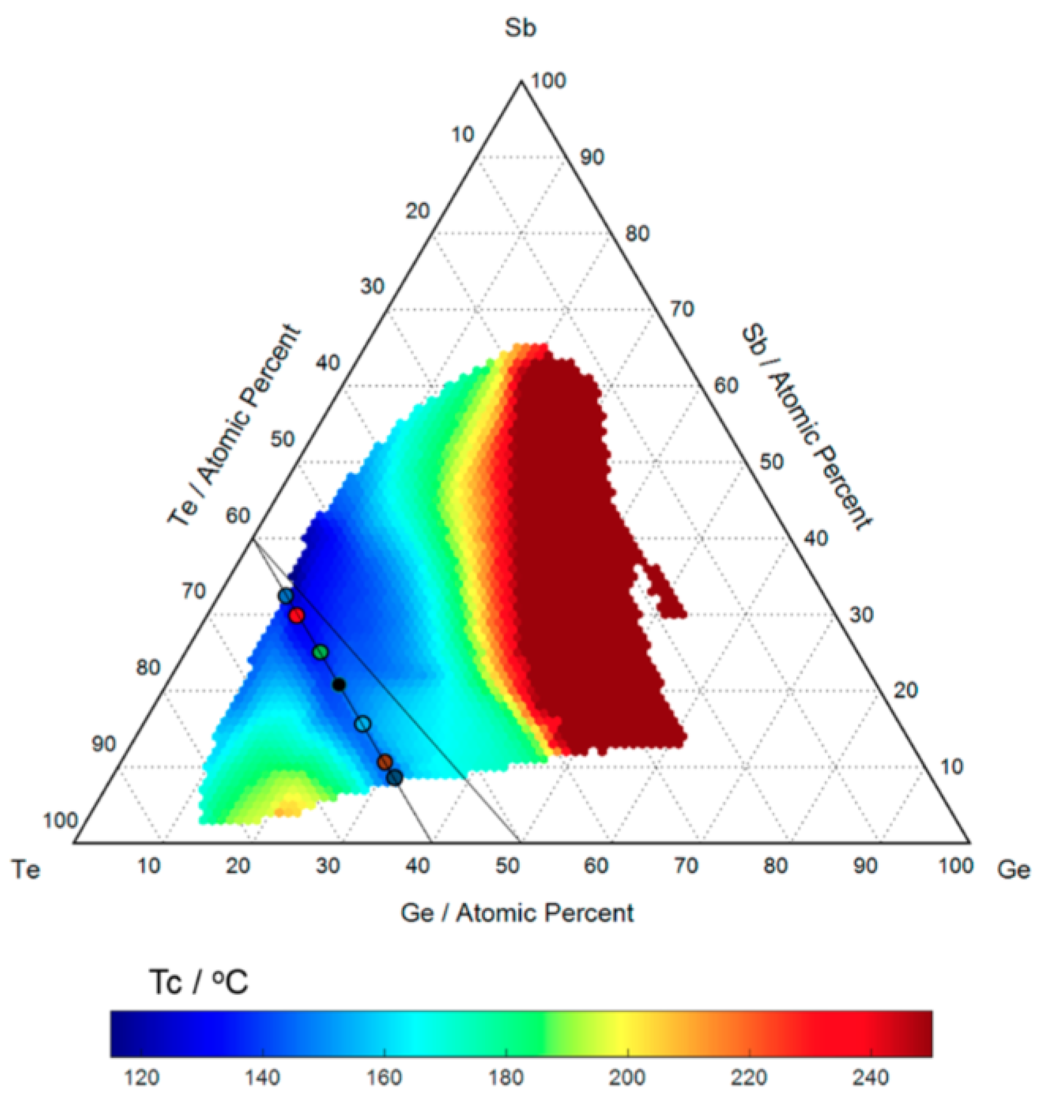
2.1. GeSbTe Alloys

Germanium-antimony-tellurium (GST) alloys are a type of phase change material from the general group of chalcogenide glasses. Within the GST alloy system - the most widely used memory materials for phase-change applications - are the GeTe-Sb 2 Te 3 pseudobinary compounds. This can be viewed as a mixture between the two binary compounds GeTe and Sb 2 Te 3 . The time lapse images from HTOMPT (high-throughput optical mapping of phase transition) of the nonisothermal crystallization measurements are used to extract the transition temperature of different compositions and shown in Figure 1. Compounds on this pseudobinary line have different behaviors due to the variation of material composition. Moving along the pseudobinary line, from Sb 2 Te 3 to GeTe, the melting point, glass transition temperature, data retention, and activation energy increase, while the crystallization speed decreases [18].
In 1979, Phillips proposed a theory explaining the effect of the number of bonds per atom (coordination number) in chalcogenide alloys [19]. When the average coordination number for a material is between 2 and 3 (preferably 2.45), the ability of this material to form an amorphous state is high. By applying this theory into the phase-changing material GST, based on the assumption that the average coordination number can be calculated from the maximum number of bonds for the atoms, the Sb2Te3 easily tends to form an amorphous state due to the coordination number being around 2.4, while is close to the ideal value. GeTe is less apt to form into an amorphous state because the coordination number is 3, which is relatively away from the ideal value [20]. Therefore, as a mixture of GeTe and Sb2Te3, the Ge-Sb-Te material becomes less apt to form an amorphous state as the proportion of GeTe increases, because of more GeTe content in the material, the greater difference between the average coordination number to the ideal number. In GeTe and GeTe-rich compounds, as indicated in the top region of the pseudobinary line, the number of excess vacancies move the Fermi energy to the region of extended states, which results in a metallic behavior. For the vacancy-rich GST compounds in the middle part of the line, the Fermi level lies in the region of localized states and the system exhibits insulating behavior. At the bottom region of the line, it becomes increasingly difficult to obtain a cubic phase experimentally. It has been found that Sb2Te3-rich compounds exhibit stable hexagonal structures with very elongated primitive cells [21].

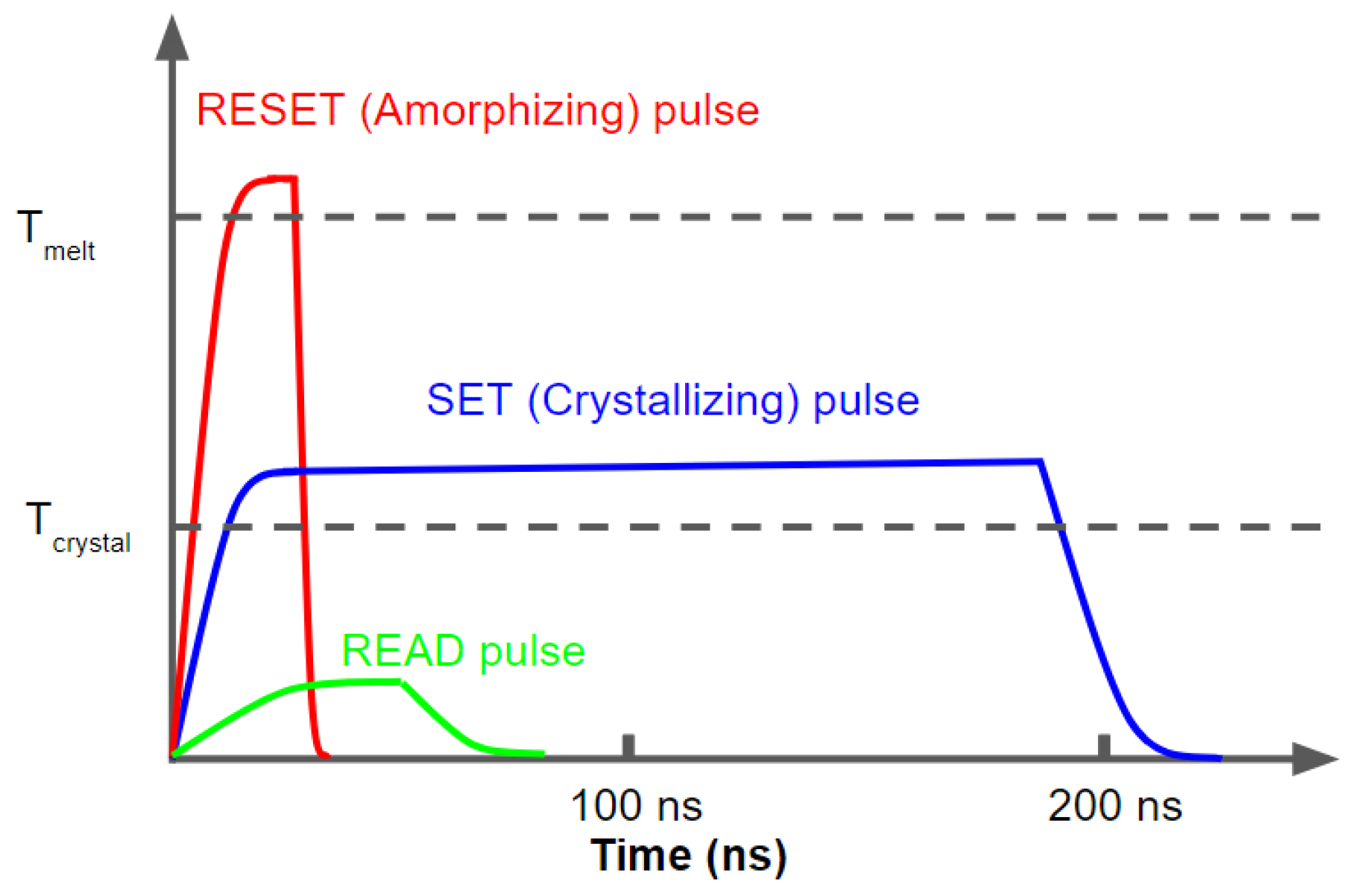
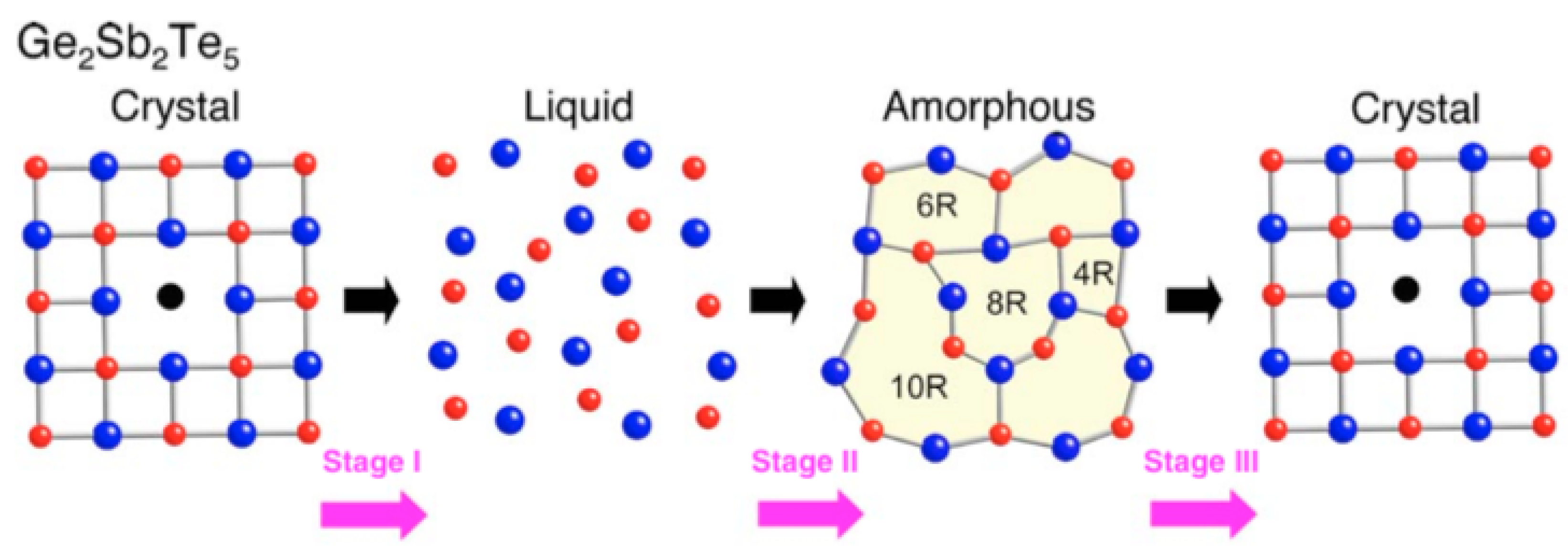
2.2. Switching Properties

In rewritable optical recording media and other PCM devices, the information storage utilizes either the large electrical or optical contrast between the two states for binary representation. As the operation for the typical memory devices shown in Figure 2, SET (conventionally linked to writing a logic ‘1’) and RESET (writing a logic ‘0’) states are controlled by a Joule heating process and are associated with amorphous-to-crystalline and crystalline-to-amorphous transitions, respectively. Since crystallization is a slower process than amorphization, the SET process in a device requires heating the material above its crystallization temperature for a sufficient length of time (tens to 100s of ns) so that the atoms rearrange themselves in crystalline order. A medium level laser or current (blue curve) for fairly long pulse times is used to re-crystallize the phase change material to its crystalline state. On the other hand, the RESET or amorphization process needs a higher temperature with a shorter duration to melt and convert the material to a liquid (amorphous) state then quickly quench the material such that the atoms do not have time to arrange in a crystalline fashion. The typical time required for RESET switching is shorter than a few tens of nanoseconds [22,23]. In this process, the temperature of the material needs to drop down quickly, i.e., the fast quench should occur faster than the timescale for thermal diffusion from cell to neighboring cell, preventing reorganization into a crystalline structure. A much lower level laser or current with essentially no Joule heating is used for reading the state, differentiating between amorphous (low reflectivity, high resistivity) and crystalline (high reflectivity, low resistivity) states.
These two approaches for switching the phase of a phase-change device, electrical and optical control, generate two formats of devices, driven by either electricity or light. For example, for PCRAM devices as in Refs. [24,25,26,27], the phase change material, and a heater element are connected in series, with the heater inducing localized Joule heating aimed at switching the volume near the interface region (between the heater and phase change material elements). We will discuss the details of PCRAMs in Section 3.1. Optical control is another effective approach that generally uses an optical pump beam that is focused on the PCM film, leading to Joule heating by absorption, which induces the phase transition. The rewritable optical disk is one of the well known optical control PCM applications [1,2].

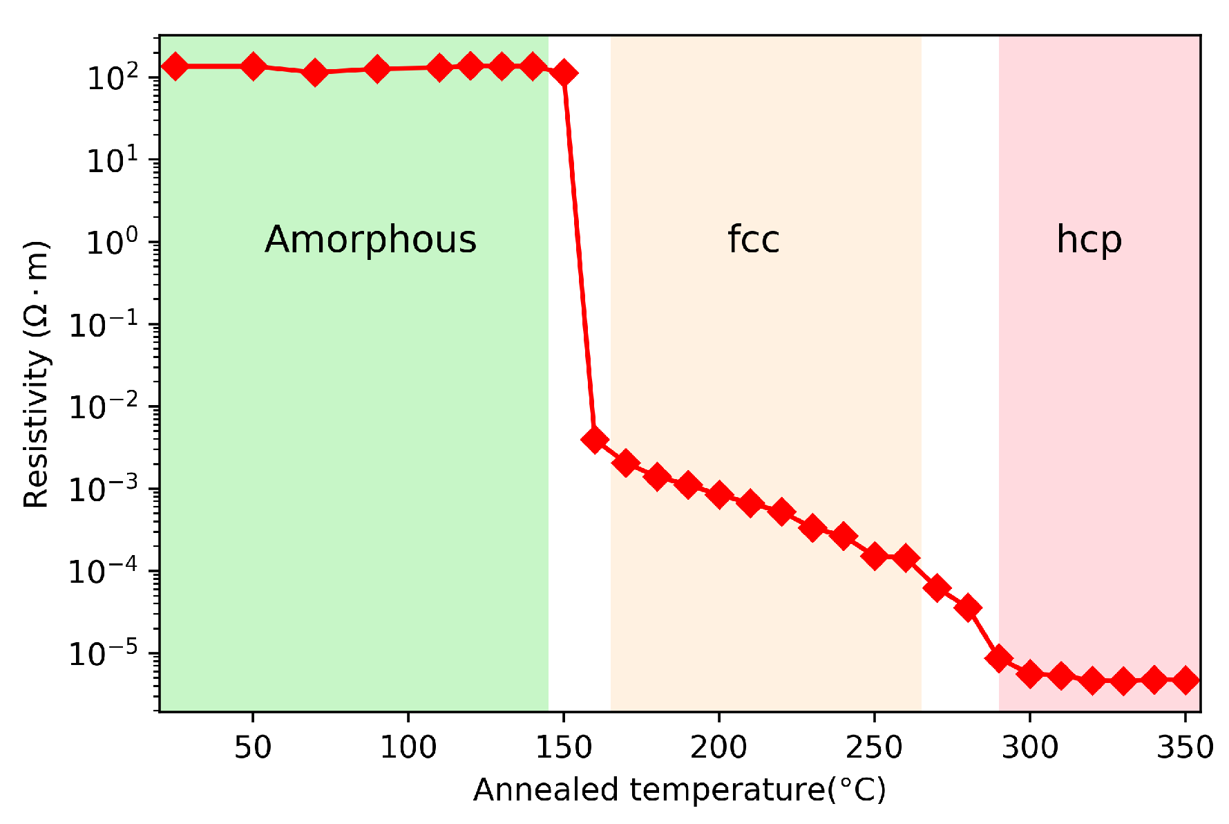
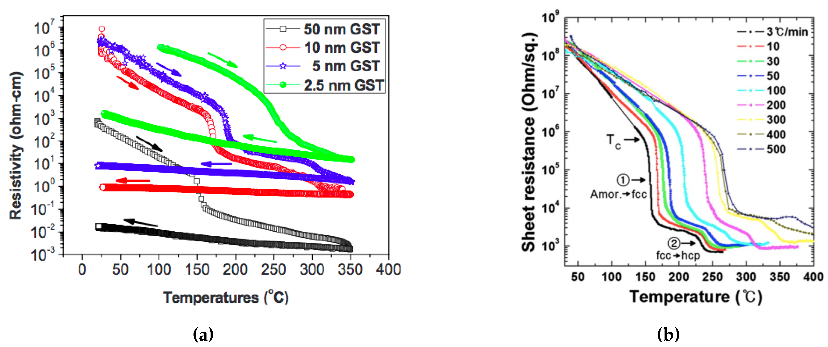
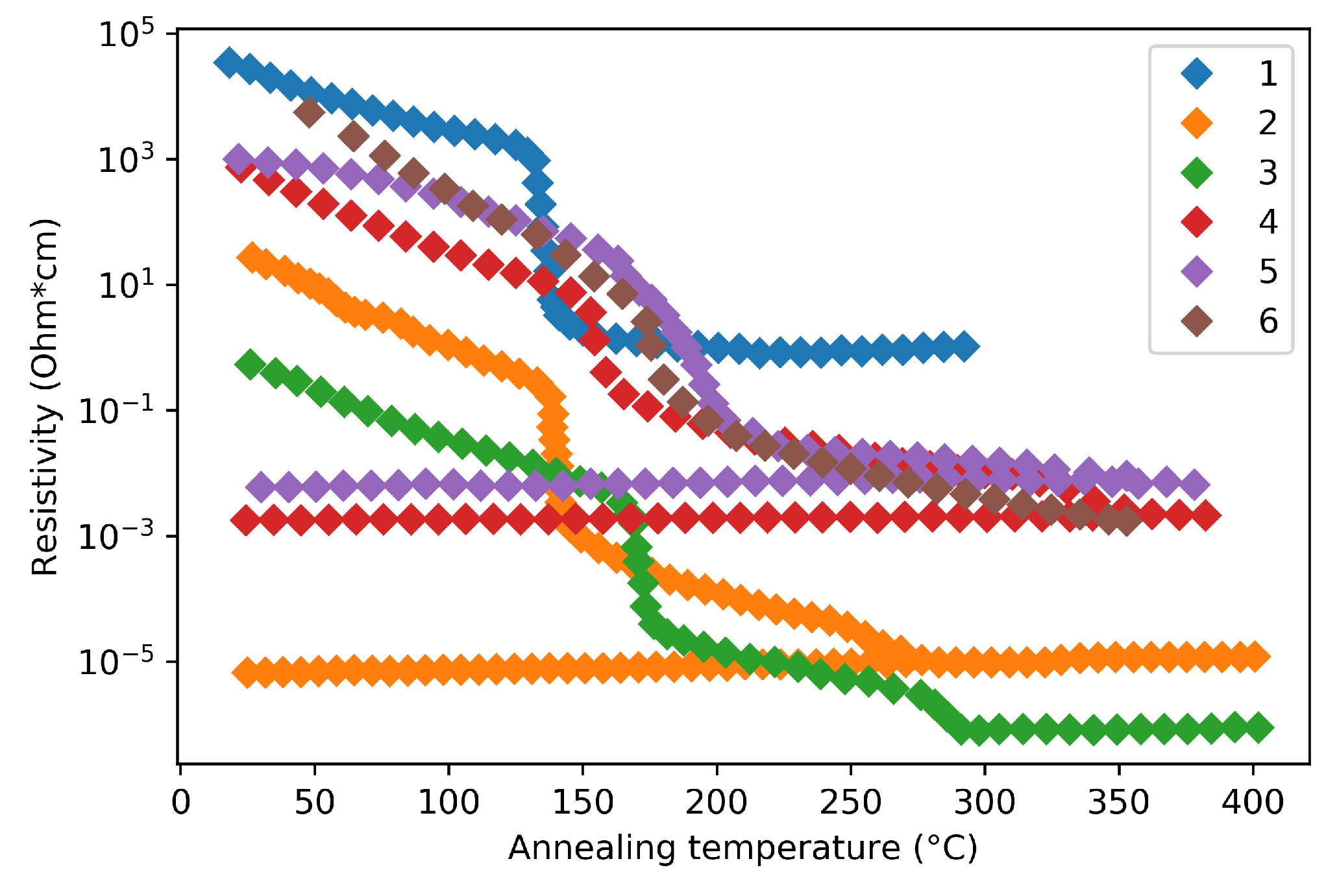
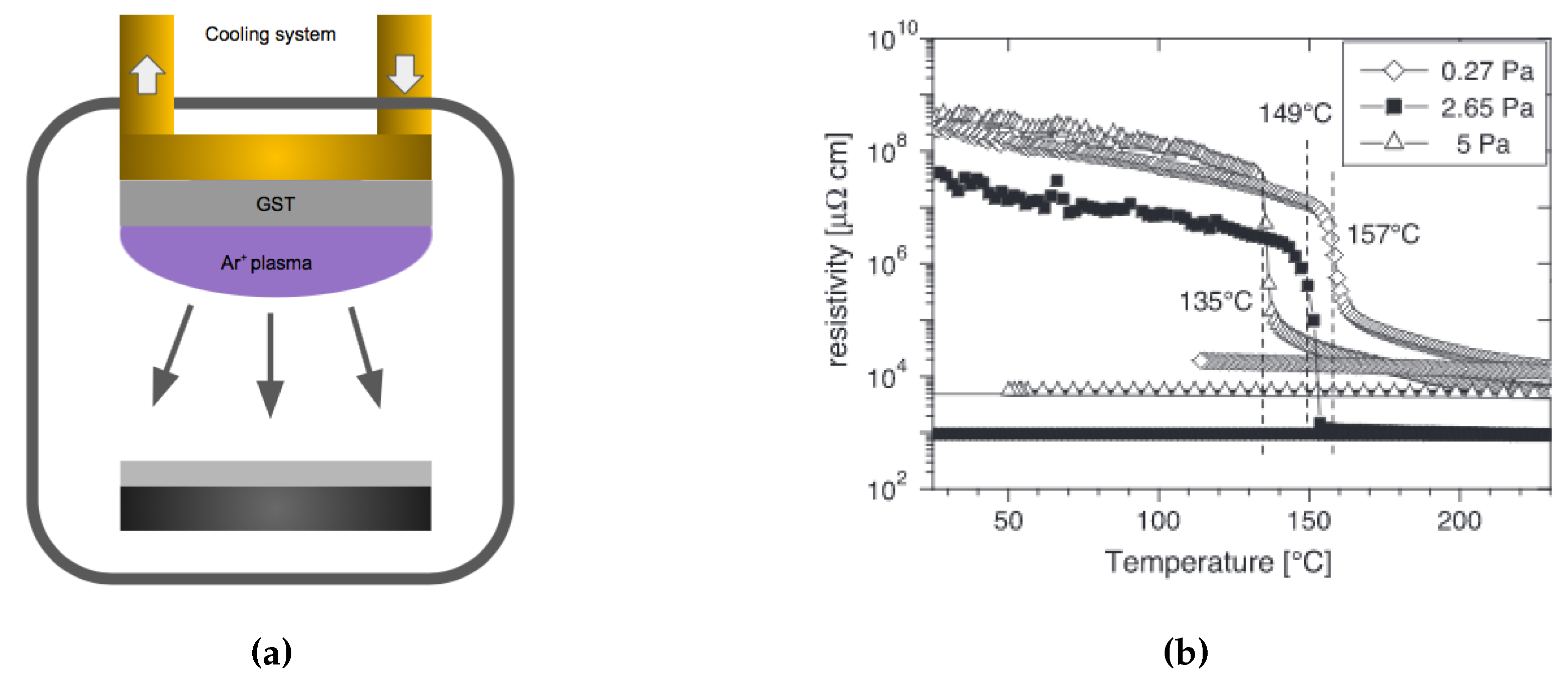
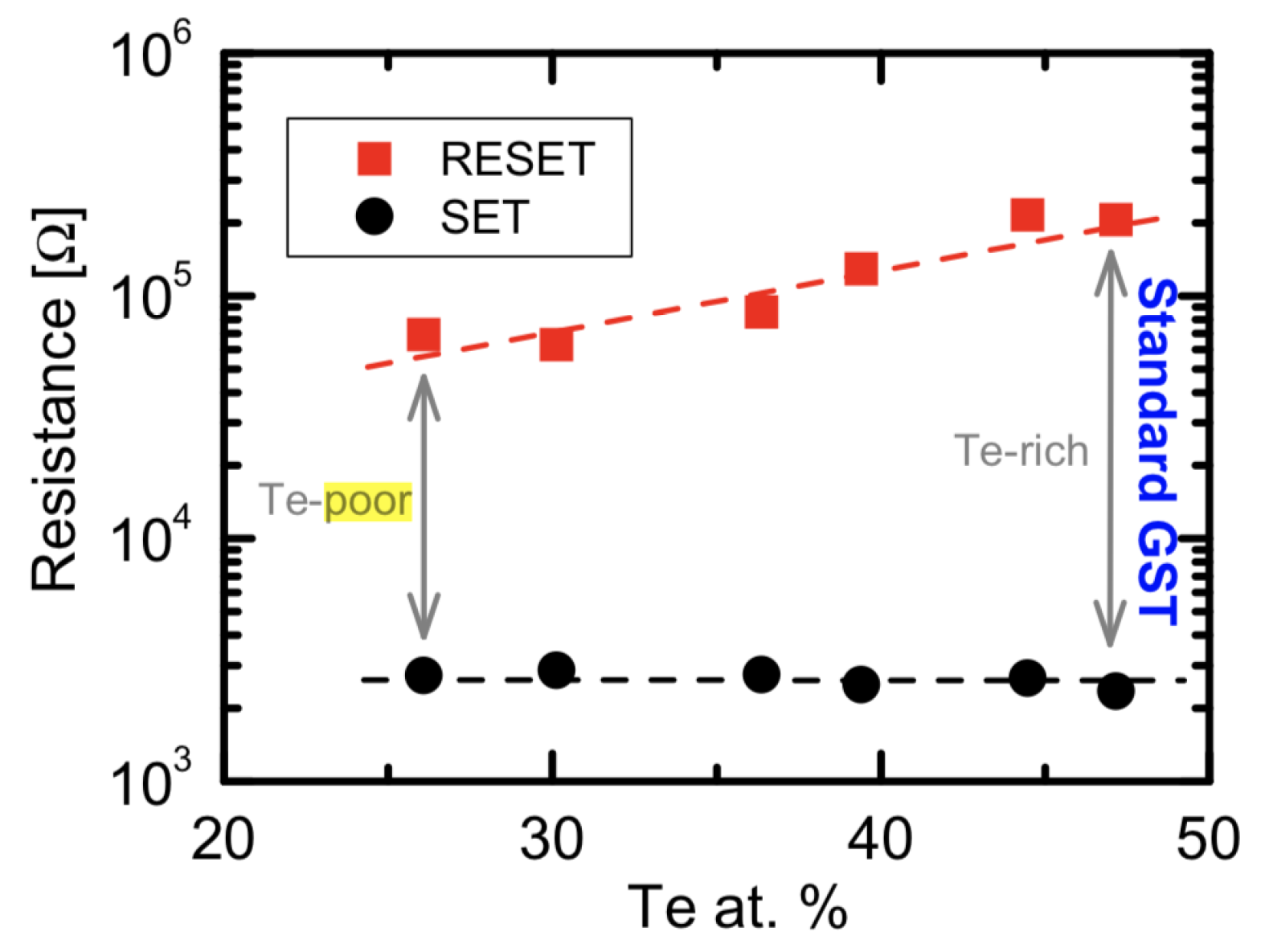
2.3. Electrical Properties

One of the fundamental properties of phase change materials is the large resistivity contrast between amorphous (high resistivity) and crystalline (low resistivity) phases. The as-deposited GST thin films are in the amorphous state. The resistivity of GST at different phases is generally characterized by a 4-point probe which is an electrical impedance measuring technique that can measure the sheet resistance of the thin films. The resistivity as a function of annealed temperature is usually used to characterize the phase transitions during the annealing process. In Figure 3, we show the resistivity of GST as a function of annealing temperature. This GST film is created by using magnetron sputtering. The sample is placed on a hot plate at discrete temperatures between 25 C to 350 C for 2 min, then the sample is cooled down to room temperature before 4-point measurement. There are two distinct transitions in the resistivity plot. The first transition near 150 C corresponds to the amorphous to face-centered-cubic (fcc) phase transition, while the second transition near 230 C is due to the fcc to hexagonal close-packed (hcp) phase [28]. The temperature dependence of resistivity has a slope between the first and second phase transition, which comes from the mixture states. Namely the mixed states between amorphous state and fcc state near the first transition, and the that of fcc and hcp states near the second transition.
The resistivity of the phase change material plays an important role since it determines the power efficiency and stability. There are several factors that can affect the phase change material’s resistivity characteristics, such as film thickness, heating rate, and fabrication methods and parameters. Figure 4a shows the effect of film thinness on the resistivity characteristic. In the very thin (less than 100nm) regime, with a smaller GST film thickness, the phase transition temperature and the resistivity at both amorphous and crystalline states increase. This phenomenon may be due to the segregation or loss of tellurium from the alloy, or it may be due to the limited amount of material available for nuclei formation as the films become very thin [29]. The problem of degradation of extremely thin films in PCMs was solved by Simpson et al. [30], where they were able to achieve broadly the same crystallization temperatures in a 2 nm GST thin film as the bulk material. In Section 3.1, we will introduce several types of modified cell structures that have been explored to circumvent this issue. Figure 4b shows the effect of heating rate on the crystallization behavior of amorphous GST thin films. The crystallization temperature from the amorphous to fcc state increases logarithmically with the heating rate. The overall effective activation energy for the crystallization is 2.34 eV at a low heating rate (less than 40 °C/minute) and 0.49 eV at a higher heating rate [31]. The difference in the effective activation energy for crystallization affects the nucleation and the growth of fcc crystalline structures.
Deposition methods and parameters can also lead to resistivity discrepancy. In fact, even the same deposition method can yield different phase transition characteristic due to the variation in experimental parameters, such as pressure and power. Therefore, the phase-change resistivity characteristics of GST thin films have been found varies between different research groups, as summarized in Figure 5.
Another critical issue is the GST degradation, most research on GST film studied on the un-sealed GST thin film which can lead to Te depletion [37,38]. The concentration of Te in the film can affect the material properties significantly. Figure 6 shows the programming window behavior as a function of tellurium atomic concentration from about 26% to 50%. With a lower tellurium percentage, the alloy experiences programming window narrowing [37]. The Te-poor alloys tend to have a lower conduction activation energies supporting a narrower energy-gap for the amorphous state, which results in a smaller resistance contrast between amorphous and crystalline states [39].

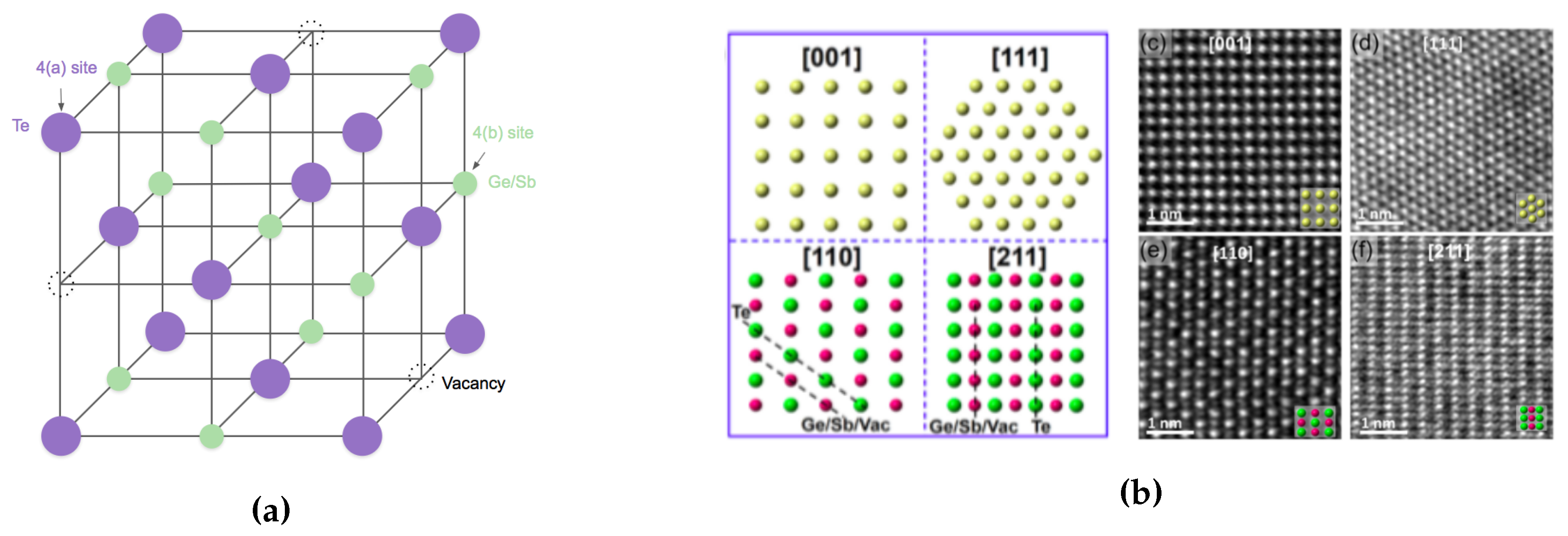
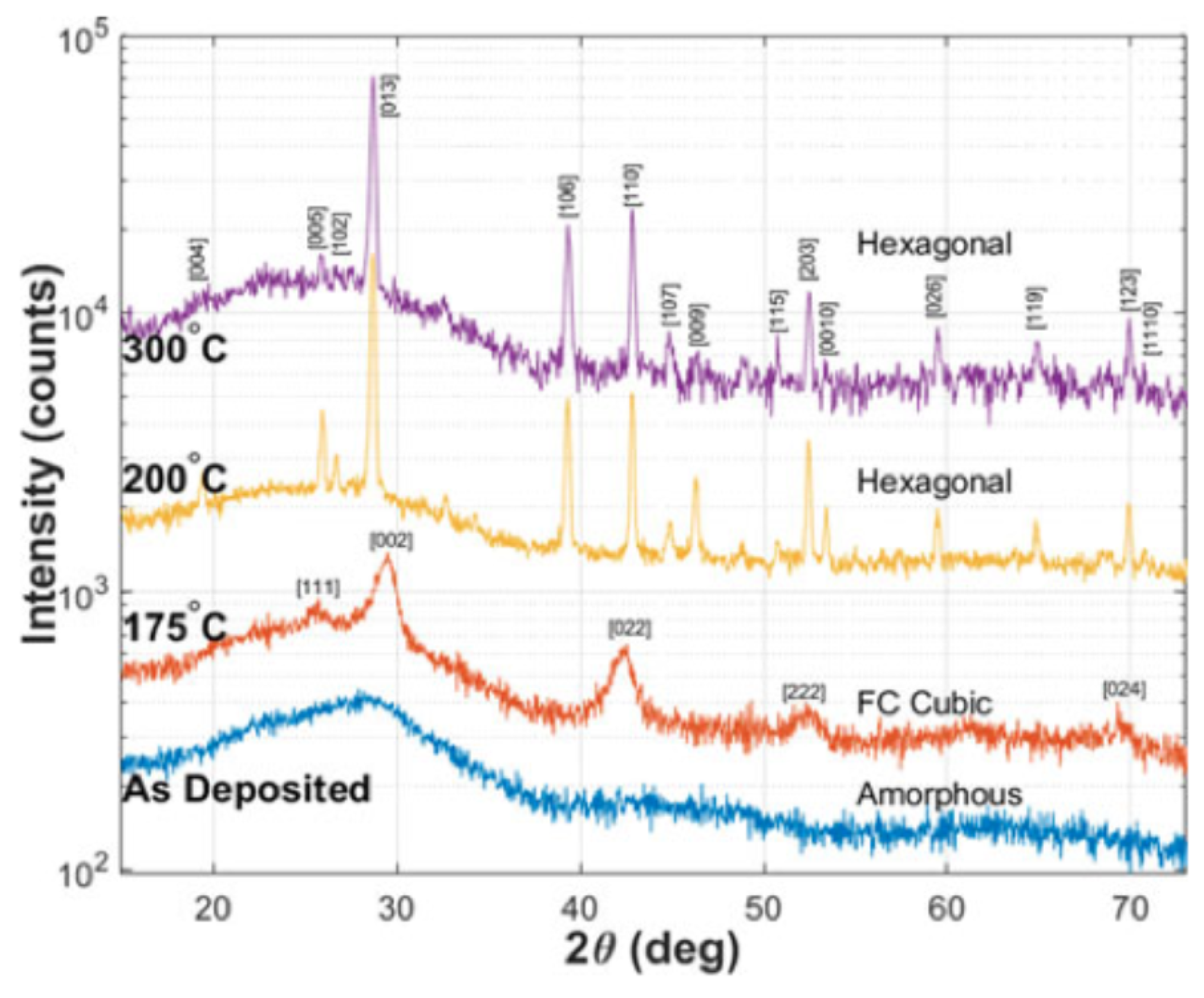
2.4. Structural Properties

It is important to understand the behavior of GST materials around the phase transition within the context of its crystal structure. Upon crystallization from the amorphous state at around 150 C , GST alloys form a poly-crystalline cubic (rock salt) state, with grain sizes of 10–20 nm. Yamada et al. proposed the crystal structure of GST at fcc state shown in Figure 7a. The 4(a) site is wholly occupied by only Te, and 4(b) site is randomly occupied by Ge, Sb atoms, with some vacancies with different probabilities depending on the composition of the materials [40,41]. Besides, the Ge2+xSb2Te5 and Ge2Sb2+xTe5 was studied by Yamada et al. [41] and Privitera et al. [42], respectively. Their results indicate the excess Ge or Sb atoms does not occupy the vacancies, but rather accumulated at grain boundaries [2]. To get a closer look of GST at the atomic level, High-Angle Annular Dark-Field Scanning Transmission Electron Microscopy (HAADF-STEM) has been used to study the crystal structures and defects of crystalline chalcogenides [43,44,45,46,47]. The atomistic models and the images obtained by HAADF-STEM on rocksalt GST are shown in Figure 7b. The bright dots correspond to the contribution of the whole atomic columns along the viewing direction, and the brightness of each dot is roughly proportional to Z 2 , where Z is the average atomic number (Ge 32, Sb 51, Te 52, vacancy 0) of the atomic column [47].
This phase-changing process of GST happens in a very short time range, as short as 50 ns. The reason for such a fast transition may because the fcc structure has a high-grade lattice symmetry which is similar to the amorphous state which has an isotropic atom distribution, indicating the composite atoms in the amorphous state do not need to travel long distances to be fixed in the fcc crystalline state [48,49]. Shinji et al. performed the reverse Monte Carlo simulation with experimental data from synchrotron-radiation x-ray diffraction [50]. Their results indicated that amorphous GST is characterized by even-folded ring structures which is the key for the fast crystallization speed. This finding is schematically depicted in Figure 8. The X-ray diffraction (XRD) is a rapid analytical technique primarily used for phase identification of GST material. The typical XRD patterns of GST thin films at amorphous, fcc and hcp states are shown in Figure 9. The film is sputtered by sputter deposition on a glass slide. The structural information is given by the peak positions and its relative intensity. Due to the nature of the amorphous state, there is no obvious peak for the as-deposited film. The film annealed at 175 is crystallized into a face-centered cubic (fcc) state indicated by XRD peaks [111], [002], [022], and [024]. Further annealing at temperatures above 175 leads to the transition from fcc structure to the hexagonal closest packed (hcp) state shown by the XRD peaks [013], [110], [203], and [026].

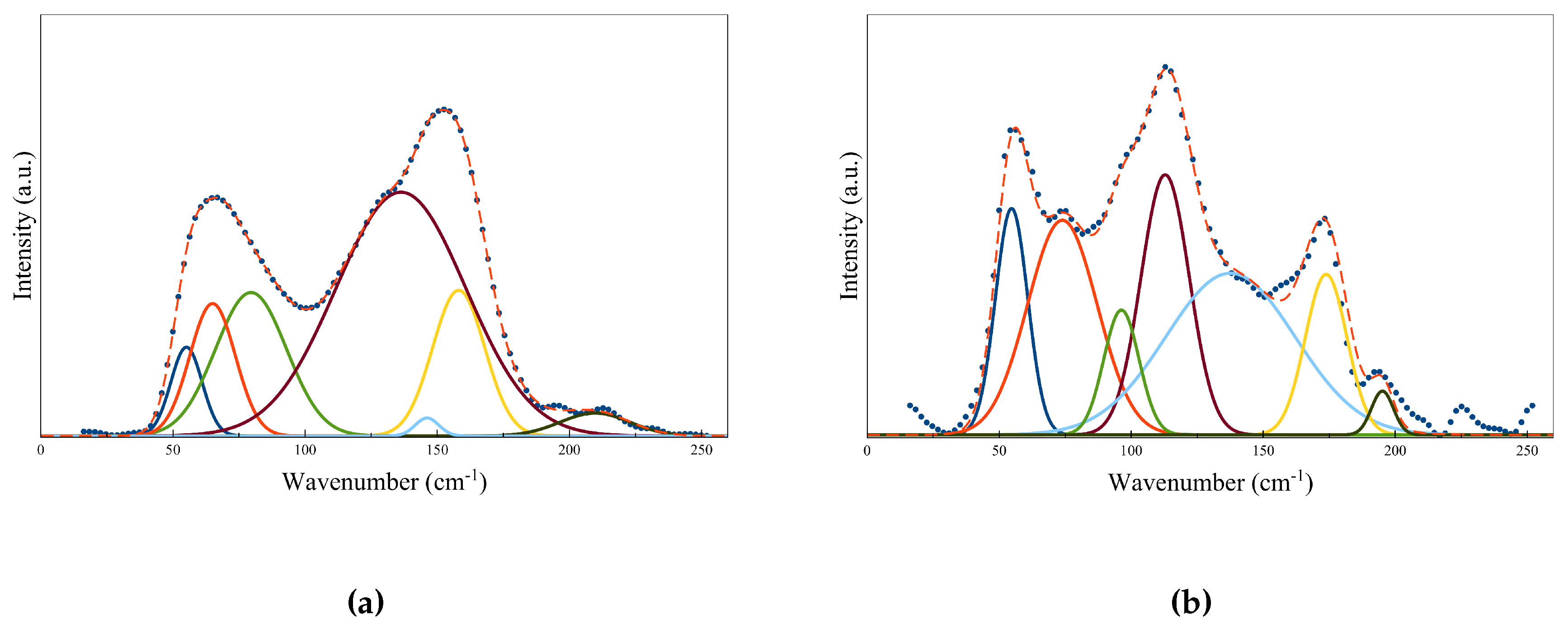
2.5. Local Structural Properties

Just as with pure semiconductors and semiconductor alloys, doping can be an effective approach to modify GST’s electrical and optical properties for a variety of applications. As such, it is important to understand how atomic substitution and distortion of the crystal occur before designing an appropriate doping scheme. To better understand those effects, it is crucial to start by studying the pure GST alloy at its local structural level. Raman spectroscopy is a typical method to characterize the local structure of both pure and doped GST at different states.
Figure 10a,b shows the Raman spectra for pure GST at both amorphous and hcp crystalline state, respectively. The local structure information was studied by decomposing the experimental Raman spectra into multiple Gaussian oscillators [51]. Different Gaussian peaks correspond to different vibration modes in the material. The peak positions are summarized in Table 2. By referring to [52,53], the peak positions of the Gaussian oscillators can be assigned as follows. The peaks at amorphous state can be attributed to defective octahedra, GeTe4-nGen (n = 0, 1, 2) edge and/or corner-sharing tetrahedra and SbTe3 pyramidal units. On the other hand, the peaks in Raman spectra for crystalline state can be assigned to defective octahedra, corner-sharing GeTe4-nGen (n = 0, 1, 2) and hexagonal Sb2Te3. Raman technique is also useful to study the doping in the local structure of GST matrix. When an element is chosen with a similar atomic radius, it is believed that doping most likely occurs via substitution. For instance, the Raman shifts by tungsten and nickel doping have been studied to provide information on the atomic substitution in the local GST matrix [51,52].

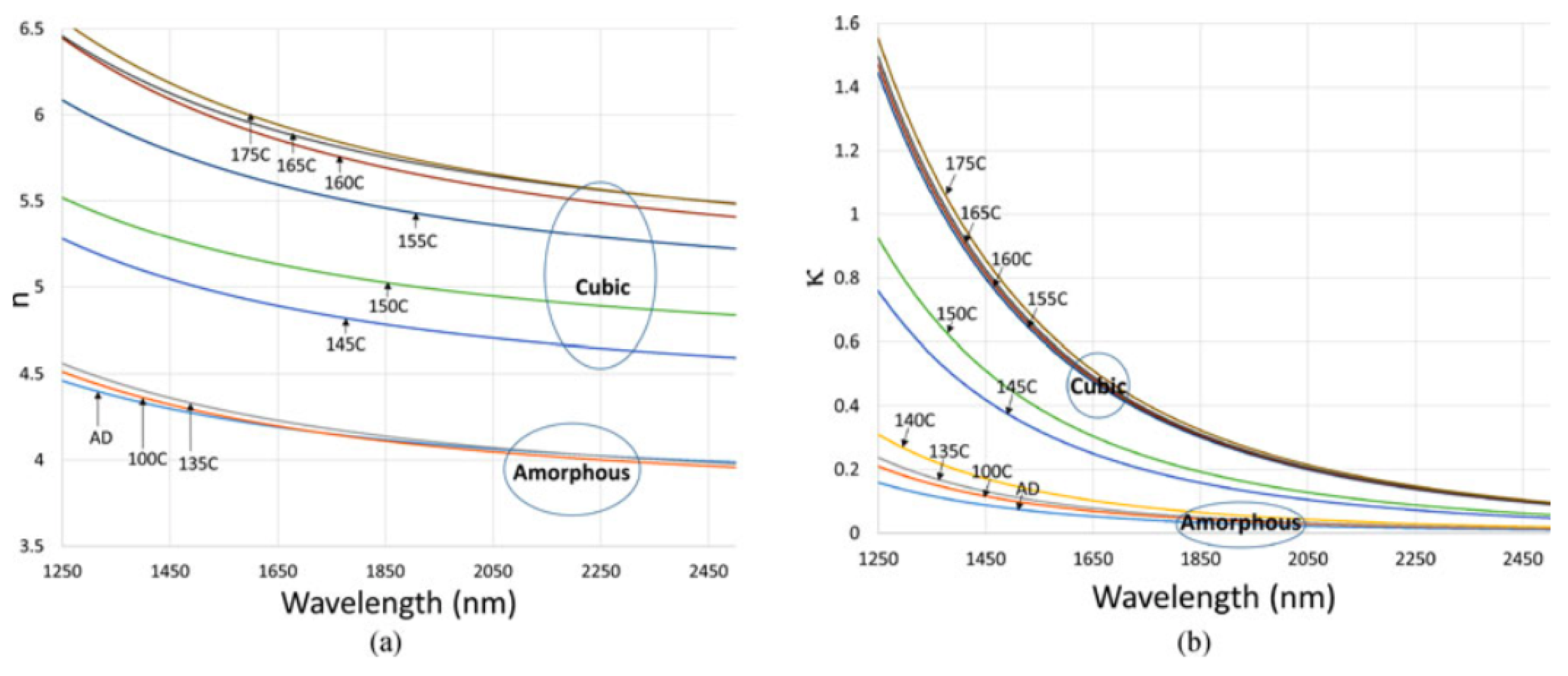
2.6. Optical Constants

The fast non-volatile phase transition of GST is accompanied by a large change of optical constants, which results in large contrast in optical reflectivity [40]. This large optical contrast is employed in optical data storage, such as rewritable DVD’s. The optical constants of GST are important in describing how the light wave interacts with the GST-based optical devices. Exact evaluation of the optical constants is critical for practical applications in integrated and free-space optical devices, such as spatial light modulators, filters, integrated modulators, and optical switches. Since the amorphous state of GST is constructed from predominantly covalent bonds, it tends to have a lower refractive index [54]. On the other hand, the large refractive index at crystalline state is a result of highly polarizable delocalized p-orbital resonant bonding [55]. Kolobov et al. demonstrate the remarkable change of the short-range order upon crystallization of amorphous GST [2] and GeTe [56] by performing the Extended x-ray-absorption fine structure spectroscopy (EXAFS) study. Since this short-range order change does not show in the conventional covalent semiconductors, suggesting the short-range order variation is related with the optical contrast in GST alloys. Wełnic et al. provided an explanation for the change of the optical absorption upon amorphization in Ge1Sb2Te4 and GeTe [57]. They conclude that the changes in the number of bonds and in the local order upon amorphization result in significant changes in the oscillator strength, which results in a profound optical contrast between amorphous and crystalline states. Shportko et al. also proposed the large optical contrast relays on the significant change in bonding which was studied by measurements of the electronic polarizability [55].
A standard technique for describing the dispersion relation in an absorbing material is through an oscillator model. the Lorentz, Harmonic, and Gaussian models as the standard and commonly used ones. For transparent materials, on the other hand, the index can be described by the Cauchy model or the Sellmeier relationship. The Cauchy model is given by:
n ( λ ) = A 0 + 10 6 A 1 λ 2 + 10 12 A 2 λ 4 + 10 18 A 3 λ 6
κ ( λ ) = B 0 + 10 6 B 1 λ 2 + 10 12 B 1 λ 4
where A, and B parameters are used to fit the refractive index of the material.
As an example, Figure 11, the fitted refractive index and extinction coefficient along the phase transition were reported [15] recently. The optical constants extraction of the optical constants was realized by fitting the measured reflection and transmission spectra from GST thin films to the above Cauchy model. The reflection and transmission of the samples in infrared were measured by Fourier-transform infrared spectroscopy (FTIR). By calculating the optical absorption coefficient, other researchers have reported similar dispersion relations for GST [58,59,60,61].
As shown in Table 3, the degree of the optical contrast change ( n c , k c - n a , k a ) at 405 nm wavelength were summarized. The larger content of Ge in the material, the higher degree of contrast in optical constants, which indicates that the GeTe-rich composition is suitable for the Blu-ray Discs from the viewpoint of optical constant [8].

3. Applications

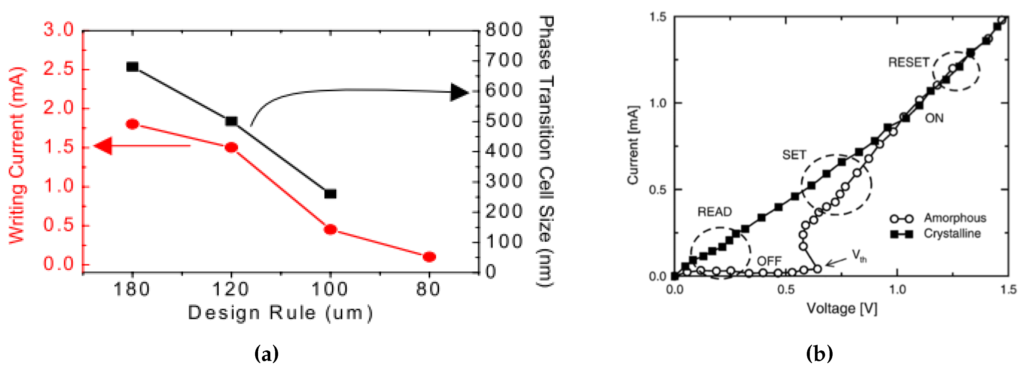
3.1. Phase-change Memory (PCM)

Nonvolatile memory devices have been the key elements for a wide variety of charge storage memories, such as flash memories, hard disk drives, and solid state drives. Even though the flash memories are widely used in the electronic products as the primary storage devices, new architectures are necessary to allow its scalability below the 16 nm technology node, due to the size limitation of flash memories [62]. Phase-change memory (PCM) has become an application of interest for non-volatile memories over the past few decades, given the simplicity of fabrication as well as the small footprint. The concept of phase-change memory originated in 1960s [63,64]. With the improvements in fabrication capability and material engineering, chalcogenide compounds, in particular, the Ge2Sb2Te5 (GST), have become the material of choice for the non-volatile phase transition memories [65,66]. Essentially, the change in electrical resistance that accompanies the change in phase is utilized as a mean of binary data representation. One of the benefits of PCM is that it offers a much faster-switching speed. Flash memories work by modulating the storage of charge. Changing the bit’s state requires removing the accumulated charge, which demands a relatively large voltage to manipulate charges. As this voltage burst requires time to build up power, the general write-times for common Flash devices is in the order of 100 μ s. In PCM devices, the memory element can be switched ON and OFF more quickly (in nanoseconds), therefore, PCM can provide much higher operation speed. Another advantage of PCM is its higher data storage stability since the information is stored in the form of structural difference instead of the electric charge in flash memories.
Depending on the size of the PCM devices, the typical pulse for the SET operation (refer to 1) has a time duration around 100–500 ns and the current is around 0.2 mA, while typical RESET (reset to 0) time is 50–100 ns with a higher current about 0.5 mA [67,68]. One of the major difficulties of the integration of PCM is that the high-density electronics requires high programming currents, especially for the RESET operation to switch the cell from crystalline to amorphous state. In fact, as shown in Figure 12a, in order to scale down the size of a PCM cell and integrate within consumer electronics, the writing current for each cell needs to be reduced down from mA to μ A [68]. The simulation results from Cho et al. [68] showed that a confined cell structure is effective in writing current reduction, footprint reduction, and contributes to a reduction in the degradation of the PCM cells over time.
As shown in Figure 12b, the resistivity of the set (crystalline) and reset (amorphous) state have large contrast below the threshold switching voltage (Vth). The largest power consumption happens at the reset programming stage since it needs to reach the melting temperature of the material. In the following sections, we will discuss the power consumption reduction by modifying the device structures (Section 3.1.1), and the phase change material itself (Section 4). It should also be noted that the resistivity of the re-amorphized state is smaller than the as-deposited amorphous state; this phenomenon can be explained through Figure 8 in Section 2.4.

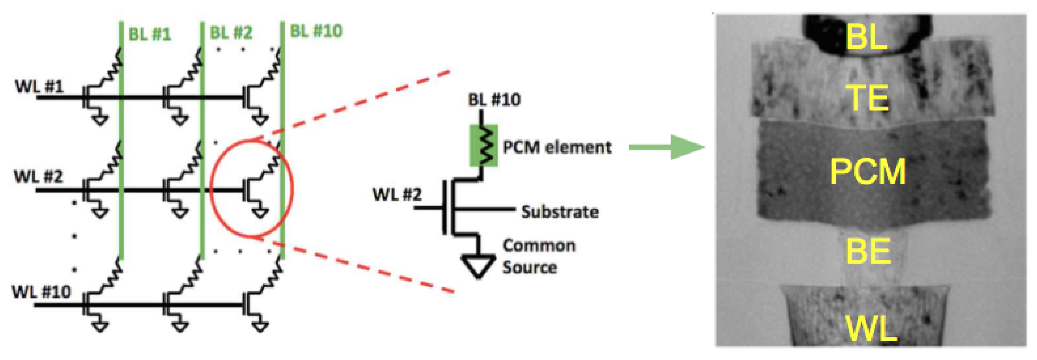
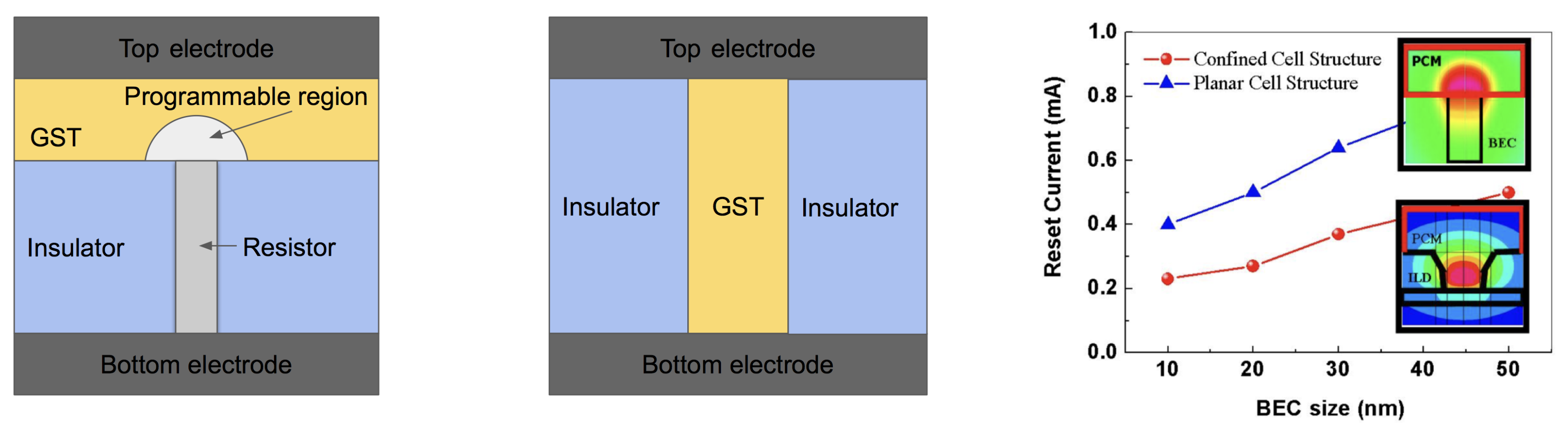
3.1.1. Device Architectures

To overcome the scaling limits for conventional Flash memory technology, one of the most attractive approach is the cross-point memory architecture, which allows for the most compact storage with 4 F 2 cell size where F is the minimum half pitch. The cross-point PCM devices generally require a selector device within each memory cell to reduce the unwanted leakage current through unselected cells during the read operation. As shown in Figure 13, each memory cell comprises a PCRAM device using a conventional mushroom-type device and a selection transistor. The cell can be accessed by a bit line connected to the gate of the transistor and a word line connected to the top electrode of PCM element [70,71]. Metal–oxide–semiconductor field-effect transistors (MOSFETs) and bipolar transistors (BJTs) are the transistors that have been used in the industry for decades for selector devices. Since MOSFETs are voltage-controlled (field driven), there is little to no power waste in MOSFETs-based selectors when powered on/idling as opposed to BJTs where a little current is consumed during power on/idling. The other advantage of MOSFETs is it only operate with one type of charge carrier, hole or electron, which leads to significant noise reduction. A 4-Mb MOSFET-selected phase-change memory was reported by Bedeschi et al. [72]. More recently, FET access devices with PCM memory cells were used to perform arithmetic operations using an accumulator-based computational scheme (computational memory) [73].
Like other resistive memories, the common PCRAM cell is a two terminal device, as shown in Figure 14 (left). It generally consists of a bottom and top electrodes, the PCM layer, and a conductive element plug (also called “resistor”, “heater”) which contributes to the heating of the phase-change material in the different phases and provides the electrical access to the phase-change material. As fabricated, the phase change material is generally in the crystalline state, since the process temperature of the (BEOL) metal interconnect layers is sufficient to crystallize the material [76].
One of the most promising approaches to the reduction of programming current is placing the PCM in a small confined structure [68], which gives a better thermal confinement of PCM and thus increasing the efficiency of Joule heating, as shown in Figure 14 (right). The bottom pillar-shaped electrode is often made of tungsten or TiN. In the case of TiN, special attention must be paid to the potential Ti-rich regions where Ti can easily chemically react with Te to produce Ti-Te compounds. Ti ions may also migrate due to the electric field during the operation. As an added benefit, the size of the phase transition cell for a confined cell structure is decreased, which enables the high storage density. In 2015, Intel and Micron jointly announced that they produced 3D Xpoint PCRAM chips with a storage capacity of 128 Gbit, and memory density of 0.62 Gb/mm 2 .
Other structures and auxiliary materials have shown a path towards hybrid optical-electrical memories. Mu et al. [78] demonstrated an electrically driven nano-scale guided wave plasmonic optical latch integrated with GST. The optimum dimensions are detailed in Figure 15. When the waveguide width is fixed to 30 nm, the thickness effect on the insertion loss is shown in Figure 15a. Figure 15b indicates a larger waveguide width can give a higher extinction ratio between ON and OFF state but suffers from a higher energy cost. Figure 15c,d denote the optimum waveguide width when both extinction ratio and energy cost are considered. Other shapes of the bottom electrode such as ring [79] or edge contact [80] have been also reported.
One of the major concerns for the highly confined structures discussed above is the fabrication and GST deposition process since it is not possible to use low-cost conventional sputtering processes due to the inherent poor step coverage. Therefore, we are going to discuss the fabrication methods that can provide good conformality, such as Metal-Organic Chemical Vapor Deposition (MOCVD) and atomic layer deposition (ALD) in Section 5.

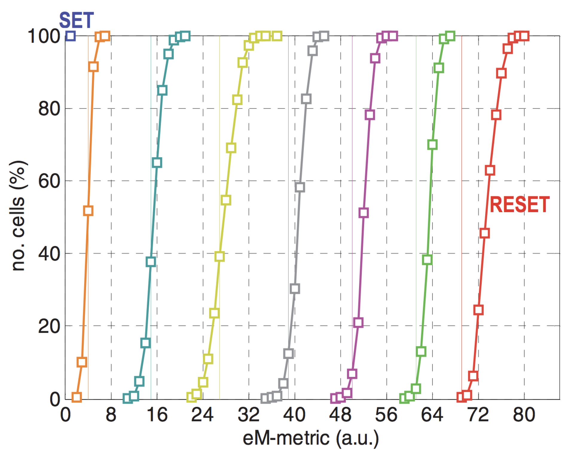
3.1.2. Multi-level Cell (MLC) Memories

Generally, in a Phase-Change Random-Access Memory (PCRAM) device, the storage of a binary 0 or a binary 1 is attributed to the amorphous and crystalline states of GST, respectively. However, by altering the temperature and the duration induced to the PCRAM cell, it is found that the resistance can set to be set to attain values in between those of crystalline and amorphous states. Based on this fact, Multi-level Cell (MLC) memories exploit these intermediate states in-between the crystalline and amorphous to store more than one bit per cell [81], which increases the memory capacity at the cell level. Therefore MLCs can effectively double or triple the data density in a memory device without increasing the footprint; each cell can store b = l o g 2 n bits of digital information, where n is the number of possible levels or states that a cell can store [82].
GST is a binary phase change material, however, by incomplete crystallization, the whole material or only crystallizing certain part of the material, over decade researchers were able to achieve numerous intermediate states between the amorphous and crystalline states [82,83,84]. As shown in Figure 16, Ref. [84] reported a 7-level cell using single pulse programming. It is crucial to note here, however, that one of the drawbacks of the MLC lies in the obvious possibility of more errors due to the reduced margin separating the states and increase in power required to program the memories.

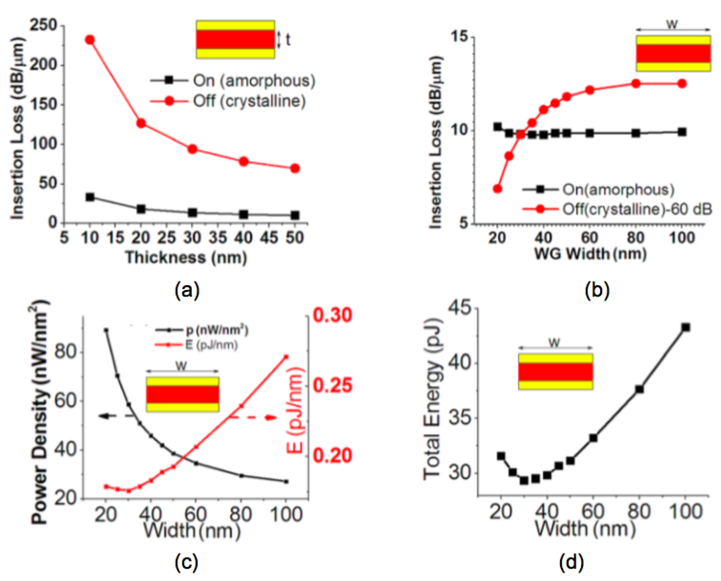
3.2. Light Modulators

Another very useful property of GST material is the large complex refractive index contrast between their amorphous and crystalline states and low loss in the infrared region [51,55,85]. This enables the writing of GST-based structures designed for telecom and mid-IR wavelengths where the losses are sufficiently low for highly versatile applications. Hendrickson et al. demonstrated a path towards electrically actuated phase-change pixels for transmissive and reflective spatial light modulators in the near and mid-infrared region.
More generally, since the optical properties of these two states in the devices differ dramatically, and this difference leads to a variety of important applications, such as, plasmonic devices [86], phase modulators [87], waveguide devices [88], chiral metamaterials [89,90], and low epsilon media [91].

3.2.1. Optical Limiters

Optical limiting has been sought after for the protection of delicate sensors and electronics from intense laser threats. Since GST has a relatively large refractive index over a broadband range, by using the GST and SiO2 as the high and low index films in a long-pass edge filter configuration, it has been possible to demonstrate the designed optical limiters has the over 30 dB extinction over a broad spectral band with ± 45 angles of incidence [15], as shown in Figure 17. The transition edge of the filter can be shifted by hundreds of nanometers by using the large refractive index difference between the amorphous and crystalline state of GST. It further demonstrates that GST can be used in multilayer configurations to realize complex optical filtering properties without inducing excessive stresses due to the phase change.

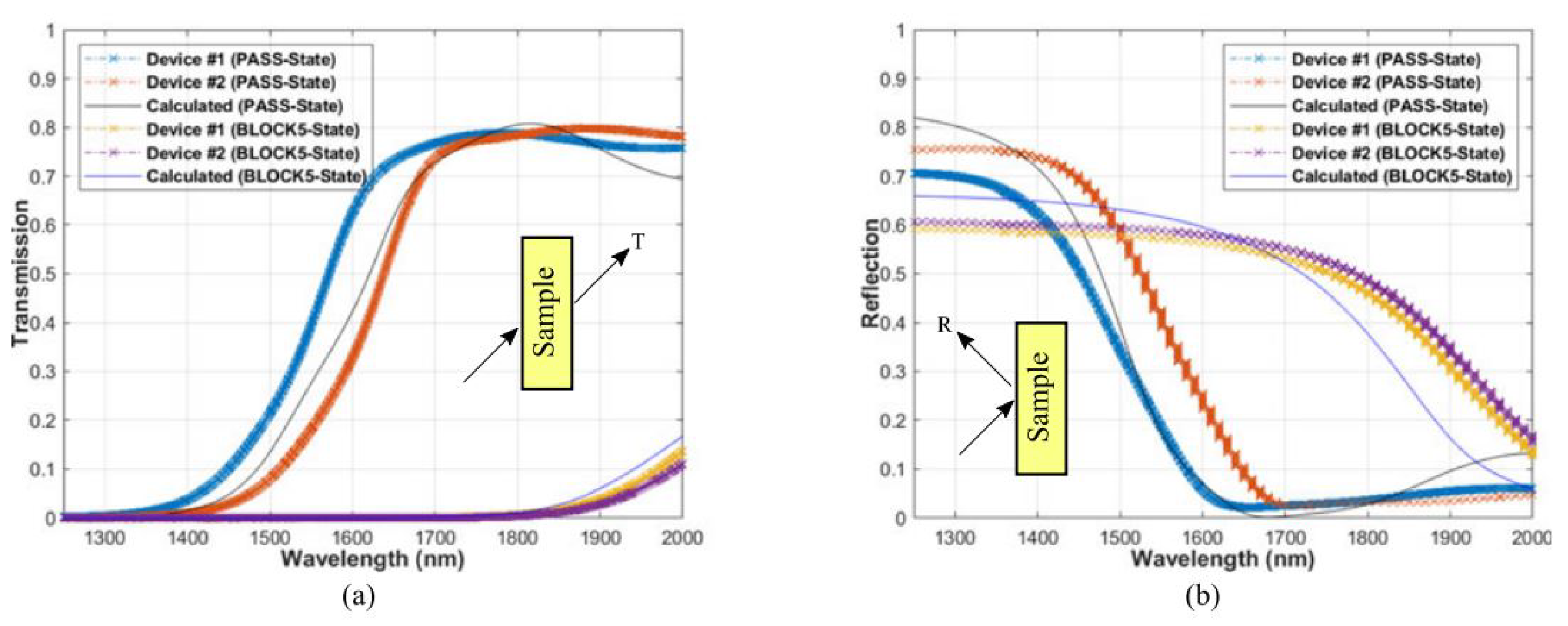
3.2.2. Meta-Surfaces

Metasurfaces or two-dimensional metamaterials where light does not typically penetrate through the surfaces have been demonstrated to have usefulness in lenses, hologram and polarization control [92,93]. However, optical loss is a common theme for all those devices, due to the metal elements in conventional metasurface devices. Another limitation is that conventional metasurfaces-based devices are not cost-effective since once a device is made, it only works for a certain functionality and wavelength. Therefore, there has been considerable interest recently in developing tunable all-dielectric metasurfaces for light modulation applications by using the phase change materials [94,95,96,97] instead of metallic elements used in earlier works.

4. Doping

GST is promising in both electrical and optical fields as discussed in the previous chapters, however, there are several issues that come to play in real applications, such as the stability of the amorphous state, power consumption and resistivity contrast in RF devices. One method to solve the problems is through doping other elements inside the GST material. A variety of elements such as C [98,99], O [100], N [100], Ni [101], Si [102], Al [103,104], Ti [105], W [52] and Cu [106] have been used to improve the device performance.

4.1. Resistivity at Amorphous State

GST has a quite large resistivity at amorphous state-several hundred Ω · m—which can limit the potential applications in the electrical devices, especially for high speeds applications. The large resistivity requires a high voltage or long wait time to dissipate sufficient power in the devices to induce the transition, as well as resulting in a large impedance difference between the amorphous and crystalline phases. In the past few years, different dopant elements have been studied to modify the electrical properties of the host GST materials. The dopant can exist in the grain boundaries to suppress the grain growth, which results in a higher transition temperature.

4.2. Amorphous State Stability

One of the main issues faced by PCRAMs and other GST-based devices is the instability of the amorphous state after repeated cycling of the phase transition. One of the methods to improve the stability is by incorporating dopant in the GST structure, such as Sn [107]. The reason for the improved stability of the amorphous state is that the material effectively becomes a multi-element material consisting of four or more elements, which can effectively suppress the movement of atoms due to different atomic radiuses and hence, increase the activation energy [20].

4.3. Operation Speed

Another challenge remaining in PCRAM technology, especially for high-speed cache-memory, is the operation speed. Generally, as the film goes thinner, the crystallization speed drops and phase transition temperature increases [29]. To increase the crystallization speed for very thin films, Yamada et al. [8] reported the Sn dopant in Ge2Sb2Te5 which could increase the crystallization speed and even a 5 nm thick film showed a crystallization time less than 50 ns. Since SnTe has a lower crystallization temperature and a higher melting point than GeTe, the probability of nucleation will be higher in amorphous SnTe than GeTe. Which means the crystallization process in GST can be accelerated by substituting Sn for Ge. Furthermore, since both SnTe and Ge2Sb2Te5 have a stable NaCl structure after crystallization, they tend to form a single-phase crystal after crystallization. It is strongly expected that Sn replaces Ge substitutionally, which is supported by the fact that both Sn and Ge belong to Group IV in the periodic table and possess relatively close atomic radii.
In 2017, Rao et al. introduced ScSbTe alloy to speed up the crystallization kinetics from tens of nanoseconds of GST down to 700 picoseconds, which comes from the reduced stochasticity of nucleation through geometrically matched and robust Sc-Te chemical bonds that stabilize crystal precursors in the amorphous state [108]. In other words, this compound geometrically matched very well to the base-alloy rock-salt crystalline product Sb 2 Te 3 , and the Sc 2 Te 3 bond is more robust as compared with Sb 2 Te 3 .

5. Deposition Methods

Different deposition methods affect the film composition, density, and stress hence the electrical and optical properties. Therefore, it is necessary to review the fabrication methods for GST. Sputtering (Section 5.1) and Pulsed Laser Deposition (PLD) (Section 5.2) tend to provide films with good density. A good conformal step coverage in fabrication means the created thin films have the same vertical and horizontal thickness. The non-conformal step coverage is good for lift-off to create GST optical device, while the conformal step coverage is critical in creating confined cell structures. Therefore, it is necessary to introduce the deposition methods for GST films that can provide a non-conformal step coverage or a good conformal step coverage. to have access to both conformal and nonconformal deposition methods. Evaporation (Section 5.3) is a typical directional deposition technique to create non-conformal step coverage which is preferred by the lift-off process. The techniques can provide good conformal step coverage include chemical vapor deposition (CVD) (Section 5.4), atomic layer deposition (ALD) (Section 5.5), and plasma enhanced chemical vapor deposition (PECVD). Evaporation is a typical directional deposition which is preferred by the lift-off process.

5.1. Sputtering

Sputtering is a widely used deposition method for a wide variety of thin films. It is particularly suited for GST because of its multi-element composite nature. Sputtering can produce high-quality dense films with preservation of the stoichiometry upon deposition. In sputtering, a target with the correct GST composition is typically used as the material source, see Figure 18a. Ar+ atoms are accelerated by an electrical field towards the target where the atomic species are sputtered out. These atoms and clusters land on the substrate to form the thin films. One of the strengths in sputtering is the preservation of the target stoichiometry, which occurs only after a certain length of time (known as target conditioning) to account for the different sputter yields of the constituent elements of the target. The sputtered films properties can be controlled by adjusting the working pressure, power, and the plasma gas. During DC sputtering, a higher argon pressure leads to a lower phase transition temperature [109], see Figure 18b. The argon gas also has an effect on the sputtered thin film surface morphology, Bakan et al. [110] reported the sputtered GST film tends to form cracks with a higher Ar flow rate (higher pressure), presumably due to the accumulation of stress. Therefore, the higher quality GST can be deposited by sputtering at a lower argon pressure.

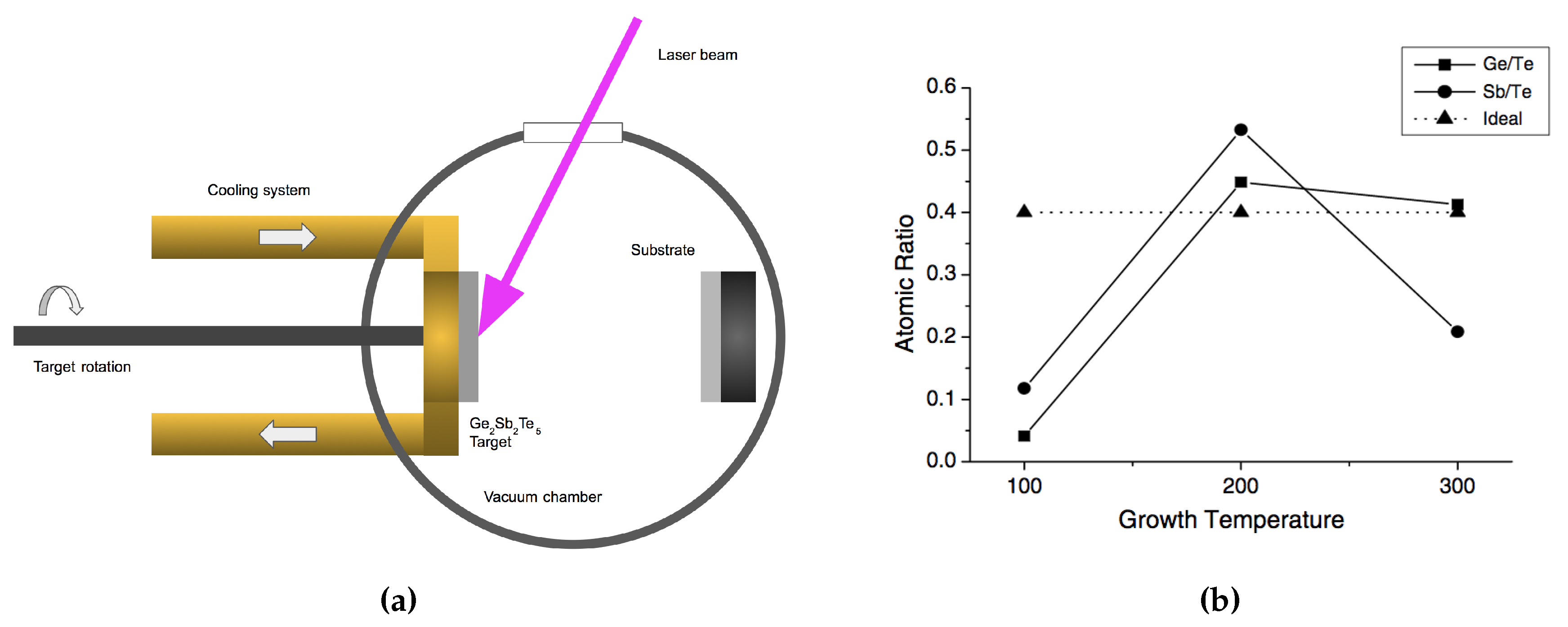
5.2. Pulsed Laser Deposition (PLD)
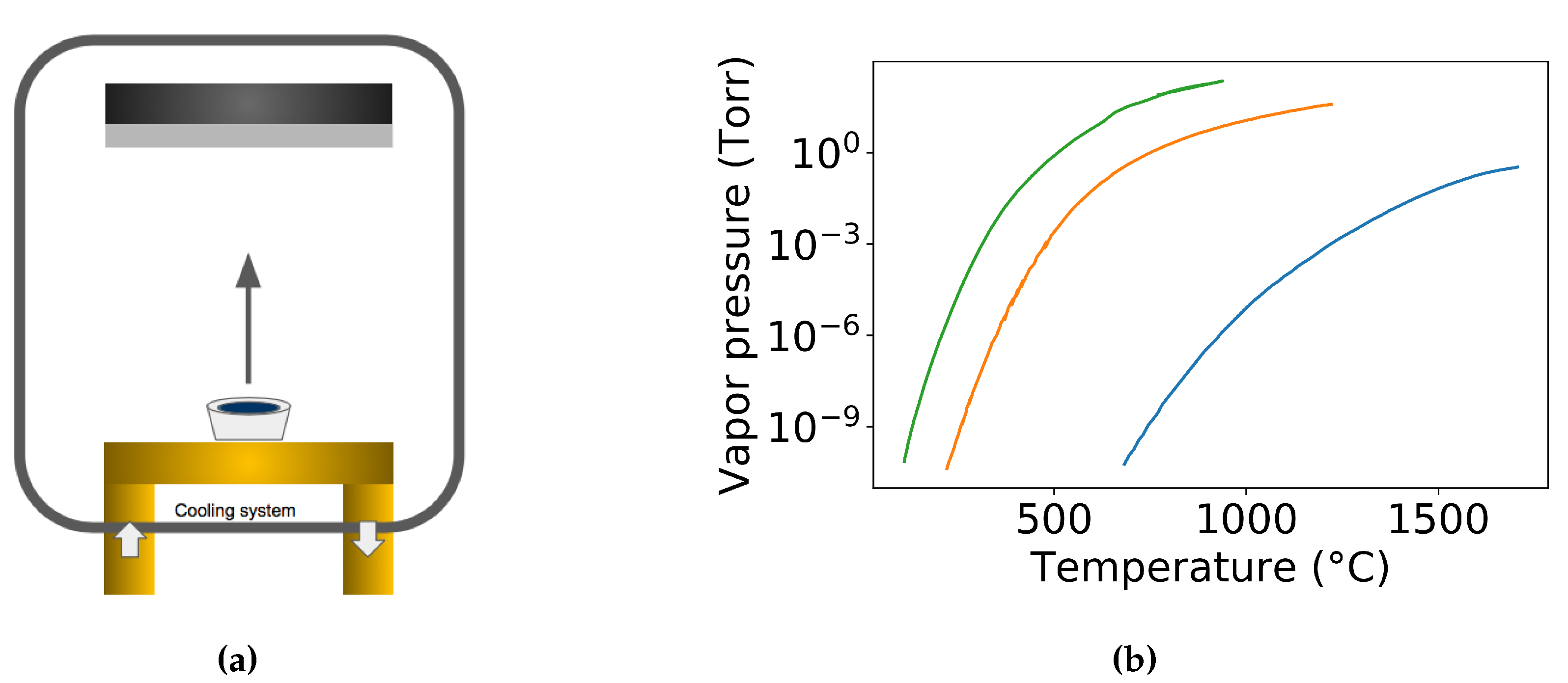
Pulsed laser deposition (PLD) is another useful deposition technique for creating GST. Like in sputtering, it enables stoichiometric transfer of target material, and the possibility of achieving congruent deposition [53,85,111]. As can be seen in Figure 19a, the GST target is irradiated by a focused laser beam through a UV-transparent window. A plasma plume forms from the irradiation spot. Both the GST target and the substrates need to be rotated during the ablation in order to avoid damaging to the target, and ensure a thickness homogeneity of the deposited films. A variety of growth conditions can be modified in a PLD system to modify the fabricated film properties, such as the temperature of heat-treatment, working pressure and laser energy. Among them, Yoon et al. studied the effect from the temperature of heat-treatment on the composition of GST nano-particles [111], as shown in Figure 19b. It is interesting to know the arriving species during the deposition. Therefore, researchers have been explored the dissociation of GST in the plasma by using mass spectroscopy [112,113]. Their finding shows the formations of single elements, binary Ge-Te, and Sb-Te compounds, and ternary non-Ge2Sb2Te5 compounds, and there may also exist other larger clusters which may lie outside the detection range of the mass spectrometer.

5.3. Evaporation

In evaporation, the arriving species to the substrate can be approximated to be strongly directional, see Figure 20a. Therefore, evaporation has the worst film conformality while it can provide the best directional deposition which is preferred by the lift-off patterning process. There are two approaches to deposit GST films in an evaporation system. One approach is to directly evaporation the Ge2Sb2Te5 alloy (Single source evaporation) [114,115], while the other method deals with the multi-source evaporation from the corresponding constituent elements [61].
In the direct evaporation process of GST, association or dissociation of the GST alloy can happen individually or simultaneously. The association does not change the stoichiometry of the deposition film from the source but may introduce new constitute from the association. However, the stoichiometry in dissociation usually changes along the deposition process. Drowart et al. performed a mass-spectroscopic investigation of the vapors to show that the molecular species normally changes during the transition from solid to the gas phase in the evaporation of compounds [117]. In the case of dissociation during the evaporation process, the compound may dissociate into smaller components that the constituents of the compounds can evaporate individually. The more volatile species in GST source tend to evaporate first, which can result in a non-congruent stoichiometry from the source, see Figure 20b. Besides, the more volatile species can also tend to be rich in the bottom of the deposited films, which can end up with a refractive index variation along the depth [118]. Mono-atomic vapor may be observed for alloys even in those cases where the pure element can form molecules. In 1966, Sommer et al. showed the exist of mono-atomic antimony vapor in the Pt−Sb [119], then in 1978 Lowe et al. found the mono-atomic antimony vapor in Au−Sb [120]. However, it is worth pointing out that due to the change in the chemical potential in the solid compound source, the vapor pressure of a compound constitute is different from that of the pure material at the same temperature [121]. The constituents of the compound remain homogeneous throughout the evaporation process. The variation of the ratio during the evaporation process depends on the stoichiometry of the initial compound. The more volatile constituent evaporates preferentially which induces a reversed proportions after the evaporation. The prepared thin films normally have a vertical stoichiometry gradient, which can modify the refractive index along the vertical direction [118]. In the direct evaporation, one has to be more careful to choose the appropriate starting concentration of the constituent to compensate for the different volatilities in order to obtain the right composition from the evaporation [122].
In the multi-source evaporation configuration, the constituents are evaporated from their corresponding sources at different temperatures and subsequently joint condenses on the substrate, which circumvents the decomposition problem as encountered in the direct evaporation of compounds. Furthermore, the multi-source evaporation technique also provides the possibility for doping. Wang et al. reported indium-doped Ge2Sb2Te5 thin films by thermal evaporating the single-element In, Ge, Sb, and Te sources [123].

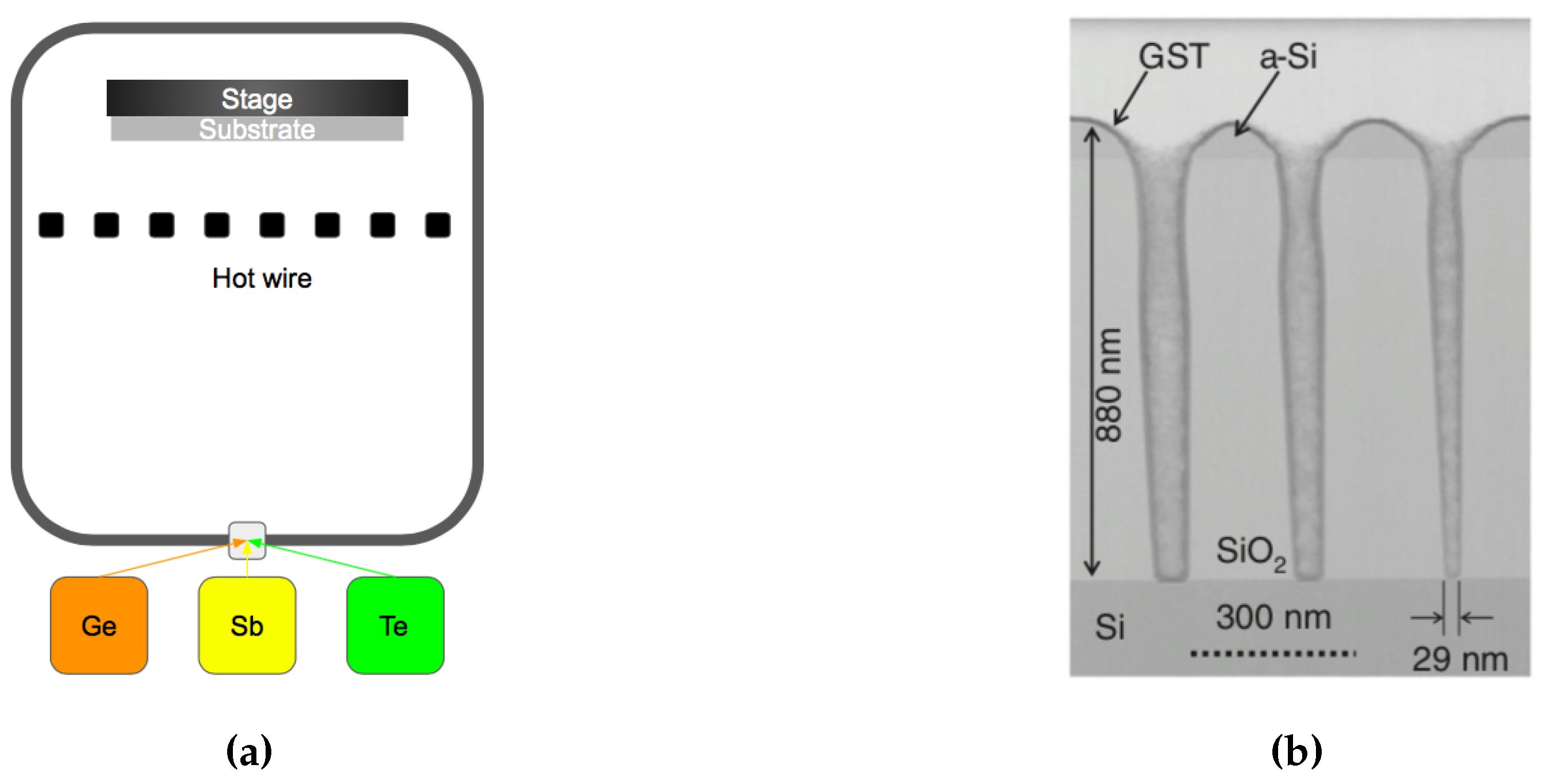
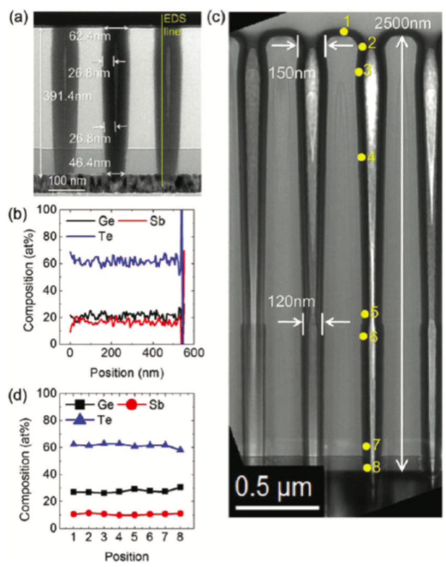
5.4. Chemical Vapor Deposition (CVD)

One of the critical challenges for creating PCM devices is the continued downscaling and the reduction of the set/reset current. The most promising approach is to move towards into 3-D architectures, where holes are first etched then filled with Ge2Sb2Te5. Unfortunately, conventional physical vapor deposition (PVD) methods, such as sputtering and evaporation, are not suitable for high-aspect-ratio filling due to the poor step coverage. Therefore, it is useful to review the deposition method that can provide better conformal coverage. Chemical vapor deposition (CVD) is based on a reaction that takes place directly on the surfaces, which leads to a good conformal step coverage on most structures. In CVD methods, alkyl and alkyl-amino compounds of Ge, Sb, and Te are used as precursors in the fabrication of GST [124,125,126]. The schematic of the CVD system is shown in Figure 21a. This method can provide a very high growth rate by using the hot-wire CVD set-up system [127], see Figure 21b. However, the atoms or the ligands introduced by the precursors can behave as contaminants in the GST-based memory cell. One drawback lies in this fabrication method is unlike the co-sputtering technique, it is a challenge for doping the GST materials in the chemical vapor deposition methods.

5.5. Atomic Layer Deposition (ALD)

In non-volatile memories, high integration density desired GST thin films with good conformality. The self-limiting film growth mechanism of Atomic Layer Deposition (ALD) ensures a superior growth conformality. This deposition method is considered as a subclass of chemical vapor deposition. In earlier demonstrations, researchers have attempted atomic layer deposition of tellurium-containing phase changing materials by using plasma-assisted, partially CVD-like process [129,130]. However, the high reactivity required in ALD for Telluride can raise safety issues. To overcome this limitation, people have developed the alkylsilyl tellurium-based ALD precursors for tellurium which is sufficiently volatile, thermally stable and highly reactive [35,131]. In 2012, Eom et al. reported a robust thermal ALD of the G–S–T films by using silyl–Te and alkoxy–Ge and alkoxy–Sb metal–organic precursors at low temperature (≈ 70 ) without using any reactive gas [132]. The cross-section transmission TEM images shows good uniformity along the contact hole surface and the composition is close to Ge2Sb2Te5, as shown in Figure 22.

6. Conclusions

Germanium-antimony-telluride has proven to be a very useful material in both the (continuously evolving) electronic as well as the (recently emerging) optical fields of study, with new technologies based on GST continuously under development. During recent decades, impressive progress has been made in the fabrication and optimization of GST-based devices. This review serves to highlight recent progress in both materials development as well as in recent device implementations, with an outlook towards both optical as well as electronic future applications.

Author Contributions

Conceptualization, I.A.; Validation, P.G., A.M.S, and I.A.; Writing—original draft preparation, P.G., A.M.S., and I.A.; Writing—review and editing P.G., A.M.S., and I.A.

Funding

This research was funded by the National Science Foundation under Grant Nos. 1710273 and 1709200 and the University of Dayton graduate school.

Acknowledgments

The authors gratefully acknowledge the support from Department of Electro-Optics and Photonics, Department of Physics, and Graduate School at the University of Dayton.

Conflicts of Interest

The authors declare no conflict of interest.

References

  1. Wuttig, M.; Yamada, N. Phase-change materials for rewriteable data storage. Nat. Mater. 2007, 6, 824. [Google Scholar] [CrossRef] [PubMed]
  2. Kolobov, A.V.; Fons, P.; Frenkel, A.I.; Ankudinov, A.L.; Tominaga, J.; Uruga, T. Understanding the phase-change mechanism of rewritable optical media. Nat. Mater. 2004, 3, 703. [Google Scholar] [CrossRef] [PubMed]
  3. Qureshi, M.K.; Srinivasan, V.; Rivers, J.A. Scalable high performance main memory system using phase-change memory technology. Acm Sigarch Comput. Archit. News 2009, 37, 24–33. [Google Scholar] [CrossRef]
  4. Yamada, N.; Ohno, E.; Akahira, N.; Nishiuchi, K.; Nagata, K.; Takao, M. High speed overwritable phase change optical disk material. Jpn. J. Appl. Phys. 1987, 26, 61. [Google Scholar] [CrossRef]
  5. Yamada, N.; Otoba, M.; Kawahara, K.; Miyagawa, N.; Ohta, H.; Akahira, N.; Matsunaga, T. Phase-change optical disk having a nitride interface layer. Jpn. J. Appl. Phys. 1998, 37, 2104. [Google Scholar] [CrossRef]
  6. Satoh, I.; Fukushima, Y.; Takagi, Y.; Azumatani, Y.; Hamasaka, H. Multi-layered Optical Disk with Track and Layer Identification. US Patent 5428597, 27 June 1995. [Google Scholar]
  7. Ohta, T. Phase-change optical memory promotes the DVD optical disk. J. Optoelectron. Adv. Mater. 2001, 3, 609–626. [Google Scholar]
  8. Yamada, N.; Kojima, R.; Uno, M.; Akiyama, T.; Kitaura, H.; Narumi, K.; Nishiuchi, K. Phase-change material for use in rewritable dual-layer optical disk. In Proceedings of the Optical Data Storage 2001, Santa Fe, NM, USA, 10 January 2002; International Society for Optics and Photonics: Washington, DC, USA, 2002; Volume 4342, pp. 55–64. [Google Scholar]
  9. Kuwahara, M.; Takehara, S.; Kashihara, Y.; Watabe, K.; Nakano, T.; Tanaka, M.; Nakamura, N.; Ohsawa, H.; Satoh, H. Experimental study of high-density rewritable optical disk using a blue-laser diode. Jpn. J. Appl. Phys. 2003, 42, 1068. [Google Scholar] [CrossRef]
  10. Nakayama, K.; Kojima, K.; Hayakawa, F.; Imai, Y.; Kitagawa, A.; Suzuki, M. Submicron nonvolatile memory cell based on reversible phase transition in chalcogenide glasses. Jpn. J. Appl. Phys. 2000, 39, 6157. [Google Scholar] [CrossRef]
  11. Lai, S.; Lowrey, T. OUM-A 180 nm nonvolatile memory cell element technology for stand alone and embedded applications. In Proceedings of the International Electron Devices Meeting. Technical Digest, Washington, DC, USA, 2–5 December 2001. [Google Scholar]
  12. Lai, S. Current status of the phase change memory and its future. In Proceedings of the IEEE International Electron Devices Meeting 2003, Washington, DC, USA, 8–10 December 2003. [Google Scholar]
  13. Yi, J.; Ha, Y.; Park, J.; Kuh, B.; Horii, H.; Kim, Y.; Park, S.; Hwang, Y.; Lee, S.; Ahn, S.; et al. Novel cell structure of PRAM with thin metal layer inserted GeSbTe. In Proceedings of the IEEE International Electron Devices Meeting 2003, Washington, DC, USA, 8–10 December 2003. [Google Scholar]
  14. Koba, I.M. High-resolution Spatial Light Modulator for 3-dimensional Holographic Display. US Patent 6819469, 16 November 2004. [Google Scholar]
  15. Sarangan, A.; Duran, J.; Vasilyev, V.; Limberopoulos, N.; Vitebskiy, I.; Anisimov, I. Broadband Reflective Optical Limiter Using GST Phase Change Material. IEEE Photonics J. 2018, 10, 1–9. [Google Scholar] [CrossRef]
  16. Gholipour, B.; Zhang, J.; MacDonald, K.F.; Hewak, D.W.; Zheludev, N.I. An all-optical, non-volatile, bidirectional, phase-change meta-switch. Adv. Mater. 2013, 25, 3050–3054. [Google Scholar] [CrossRef] [PubMed]
  17. Sieber, P.E.; Werner, D.H. Reconfigurable broadband infrared circularly polarizing reflectors based on phase changing birefringent metasurfaces. Opt. Express 2013, 21, 1087–1100. [Google Scholar] [CrossRef] [PubMed]
  18. Guerin, S.; Hayden, B.; Hewak, D.W.; Vian, C. Synthesis and screening of phase change chalcogenide thin film materials for data storage. ACS Comb. Sci. 2017, 19, 478–491. [Google Scholar] [CrossRef] [PubMed]
  19. Phillips, J.C. Topology of covalent non-crystalline solids I: Short-range order in chalcogenide alloys. J. Non-Cryst. Solids 1979, 34, 153–181. [Google Scholar] [CrossRef]
  20. Ueno, O.; Kobayashi, H. Optical Recording Medium. US Patent 5254382, 19 October 1993. [Google Scholar]
  21. Zhang, W.; Wuttig, M.; Mazzarello, R. Effects of stoichiometry on the transport properties of crystalline phase-change materials. Sci. Rep. 2015, 5, 13496. [Google Scholar] [CrossRef] [PubMed]
  22. Peng, C.; Mansuripur, M. Amorphization induced by subnanosecond laser pulses in phase-change optical recording media. Appl. Opt. 2004, 43, 4367–4375. [Google Scholar] [CrossRef] [PubMed]
  23. Loke, D.; Lee, T.; Wang, W.; Shi, L.; Zhao, R.; Yeo, Y.; Chong, T.; Elliott, S. Breaking the speed limits of phase-change memory. Science 2012, 336, 1566–1569. [Google Scholar] [CrossRef] [PubMed]
  24. Ovshinsky, S.R.; Hudgens, S.J.; Czubatyj, W.; Strand, D.A.; Wicker, G.C. Electrically Erasable Phase Change Memory. US Patent 5166758, 24 November 1992. [Google Scholar]
  25. Reinberg, A.R.; Zahorik, R.C. Small Electrode for a Chalcogenide Switching Device and Method for Fabricating Same. US Patent 5952671, 14 September 1999. [Google Scholar]
  26. Pirovano, A.; Lacaita, A.L.; Benvenuti, A.; Pellizzer, F.; Bez, R. Electronic switching in phase-change memories. IEEE Trans. Electron Devices 2004, 51, 452–459. [Google Scholar] [CrossRef]
  27. Yang, J.J.; Strukov, D.B.; Stewart, D.R. Memristive devices for computing. Nat. Nanotechnol. 2013, 8, 13. [Google Scholar] [CrossRef] [PubMed]
  28. Kato, T.; Tanaka, K. Electronic properties of amorphous and crystalline Ge2Sb2Te5 films. Jpn. J. Appl. Phys. 2005, 44, 7340. [Google Scholar] [CrossRef]
  29. Cheng, H.Y.; Raoux, S.; Chen, Y.C. The impact of film thickness and melt-quenched phase on the phase transition characteristics of Ge2Sb2Te5. J. Appl. Phys. 2010, 107, 074308. [Google Scholar] [CrossRef]
  30. Simpson, R.; Krbal, M.; Fons, P.; Kolobov, A.; Tominaga, J.; Uruga, T.; Tanida, H. Toward the ultimate limit of phase change in Ge2Sb2Te5. Nano lett. 2009, 10, 414–419. [Google Scholar] [CrossRef] [PubMed]
  31. Choi, Y.; Jung, M.; Lee, Y.K. Effect of heating rate on the activation energy for crystallization of amorphous Ge2Sb2Te5 thin film. Electrochem. Solid-State Lett. 2009, 12, F17–F19. [Google Scholar] [CrossRef]
  32. Lazarenko, P.; Sherchenkov, A.; Kozyukhin, S.; Babich, A.; Timoshenkov, S.; Gromov, D.; Shuliatyev, A.; Redichev, E. Electrical Properties of the Ge2Sb2Te5 Thin Films for Phase Change Memory Application; AIP Publishing: New York, NY, USA, 2016; Volume 1727, p. 020013. [Google Scholar]
  33. Kiouseloglou, A.; Navarro, G.; Sousa, V.; Persico, A.; Roule, A.; Cabrini, A.; Torelli, G.; Maitrejean, S.; Reimbold, G.; De Salvo, B.; et al. A novel programming technique to boost low-resistance state performance in Ge-rich GST phase change memory. IEEE Trans. Electron. Devices 2014, 61, 1246–1254. [Google Scholar] [CrossRef]
  34. Zhu, Y.; Zhang, Z.; Song, S.; Xie, H.; Song, Z.; Li, X.; Shen, L.; Li, L.; Wu, L.; Liu, B. Ni-doped GST materials for high speed phase change memory applications. Mater. Res. Bull. 2015, 64, 333–336. [Google Scholar] [CrossRef]
  35. Leskelä, M.; Pore, V.; Hatanpää, T.; Heikkilä, M.; Ritala, M.; Schrott, A.; Raoux, S.; Rossnagel, S. Atomic layer deposition of materials for phase-change memories. ECS Trans. 2009, 25, 399–407. [Google Scholar]
  36. Fallica, R.; Battaglia, J.L.; Cocco, S.; Monguzzi, C.; Teren, A.; Wiemer, C.; Varesi, E.; Cecchini, R.; Gotti, A.; Fanciulli, M. Thermal and electrical characterization of materials for phase-change memory cells. J. Chem. Eng. Data 2009, 54, 1698–1701. [Google Scholar]
  37. Boniardi, M.; Redaelli, A. Phase Change Memory: Device scaling and challenges for material engineering in the GeSbTe compound system. Microelectron. Eng. 2015, 137, 1–4. [Google Scholar] [CrossRef]
  38. D’Arrigo, G.; Mio, A.M.; Boniardi, M.; Redaelli, A.; Varesi, E.; Privitera, S.; Pellegrino, G.; Spinella, C.; Rimini, E. Crystallization properties of Sb-rich GeSbTe alloys by in-situ morphological and electrical analysis. Mater. Sci. Semicond. Process. 2017, 65, 100–107. [Google Scholar] [CrossRef]
  39. Boniardi, M.; Redaelli, A.; Tortorelli, I.; Lavizzari, S.; Pirovano, A.; Pellizzer, F.; Varesi, E.; Erbetta, D.; Bresolin, C.; Modelli, A.; et al. Electrical and thermal behavior of Tellurium poor GeSbTe compounds for phase change memory. In Proceedings of the 2012 4th IEEE International Memory Workshop, Milan, Italy, 20–23 May 2012; pp. 1–3. [Google Scholar]
  40. Yamada, N. Erasable phase-change optical materials. MRS Bull. 1996, 21, 48–50. [Google Scholar] [CrossRef]
  41. Yamada, N.; Matsunaga, T. Structure of laser-crystallized Ge2Sb2+xTe5 sputtered thin films for use in optical memory. J. Appl. Phys. 2000, 88, 7020–7028. [Google Scholar] [CrossRef]
  42. Privitera, S.; Rimini, E.; Bongiorno, C.; Zonca, R.; Pirovano, A.; Bez, R. Crystallization and phase separation in Ge2Sb2+xTe5 thin films. J. Appl. Phys. 2003, 94, 4409–4413. [Google Scholar] [CrossRef]
  43. Pennycook, S.J. A scan through the history of STEM. In Scanning Transmission Electron Microscopy; Springer: New York, NY, USA, 2011; pp. 1–90. [Google Scholar]
  44. Jiang, Y.; Wang, Y.; Sagendorf, J.; West, D.; Kou, X.; Wei, X.; He, L.; Wang, K.L.; Zhang, S.; Zhang, Z. Direct atom-by-atom chemical identification of nanostructures and defects of topological insulators. Nano Lett. 2013, 13, 2851–2856. [Google Scholar] [CrossRef] [PubMed]
  45. Rao, F.; Song, Z.; Cheng, Y.; Liu, X.; Xia, M.; Li, W.; Ding, K.; Feng, X.; Zhu, M.; Feng, S. Direct observation of titanium-centered octahedra in titanium–antimony–tellurium phase-change material. Nat. Commun. 2015, 6, 10040. [Google Scholar] [CrossRef] [PubMed]
  46. Zheng, Y.; Xia, M.; Cheng, Y.; Rao, F.; Ding, K.; Liu, W.; Jia, Y.; Song, Z.; Feng, S. Direct observation of metastable face-centered cubic Sb2Te3 crystal. Nano Res. 2016, 9, 3453–3462. [Google Scholar] [CrossRef]
  47. Zhang, B.; Zhang, W.; Shen, Z.; Chen, Y.; Li, J.; Zhang, S.; Zhang, Z.; Wuttig, M.; Mazzarello, R.; Ma, E.; et al. Element-resolved atomic structure imaging of rocksalt Ge2Sb2Te5 phase-change material. Appl. Phys. Lett. 2016, 108, 191902. [Google Scholar] [CrossRef]
  48. Chen, M.; Rubin, K.A.; Barton, R. Compound materials for reversible, phase-change optical data storage. Appl. Phys. Lett. 1986, 49, 502–504. [Google Scholar] [CrossRef]
  49. Yamada, N.; Ohno, E.; Nishiuchi, K.; Akahira, N.; Takao, M. Rapid-phase transitions of GeTe-Sb2Te3 pseudobinary amorphous thin films for an optical disk memory. J. Appl. Phys. 1991, 69, 2849–2856. [Google Scholar] [CrossRef]
  50. Kohara, S.; Kato, K.; Kimura, S.; Tanaka, H.; Usuki, T.; Suzuya, K.; Tanaka, H.; Moritomo, Y.; Matsunaga, T.; Yamada, N.; et al. Structural basis for the fast phase change of Ge2Sb2Te5: Ring statistics analogy between the crystal and amorphous states. Appl. Phys. Lett. 2006, 89, 201910. [Google Scholar] [CrossRef]
  51. Guo, P.; Sevison, G.A.; Burrow, J.A.; Agha, I.; Sarangan, A. Electrical and optical properties of nickel-doped Ge2Sb2Te5 films produced by magnetron co-sputtering. In Nanoengineering: Fabrication, Properties, Optics, and Devices XV; International Society for Optics and Photonics: Washington, DC, USA, 2018; Volume 10730, p. 107300L. [Google Scholar]
  52. Guo, S.; Hu, Z.; Ji, X.; Huang, T.; Zhang, X.; Wu, L.; Song, Z.; Chu, J. Temperature and concentration dependent crystallization behavior of Ge 2 Sb 2 Te 5 phase change films: tungsten doping effects. RSC Adv. 2014, 4, 57218–57222. [Google Scholar] [CrossRef]
  53. Němec, P.; Nazabal, V.; Moréac, A.; Gutwirth, J.; Beneš, L.; Frumar, M. Amorphous and crystallized Ge–Sb–Te thin films deposited by pulsed laser: Local structure using Raman scattering spectroscopy. Mater. Chem. Phys. 2012, 136, 935–941. [Google Scholar] [CrossRef]
  54. Cao, T.; Zhang, L.; Simpson, R.E.; Cryan, M.J. Mid-infrared tunable polarization-independent perfect absorber using a phase-change metamaterial. J. Opt. Soc. Am. B 2013. [Google Scholar] [CrossRef]
  55. Shportko, K.; Kremers, S.; Woda, M.; Lencer, D.; Robertson, J.; Wuttig, M. Resonant bonding in crystalline phase-change materials. Nat. Mater. 2008, 7, 653–658. [Google Scholar] [CrossRef] [PubMed]
  56. Kolobov, A.; Fons, P.; Tominaga, J.; Ankudinov, A.; Yannopoulos, S.; Andrikopoulos, K. Crystallization-induced short-range order changes in amorphous GeTe. J. Phys. Condens. Matter 2004, 16, S5103. [Google Scholar] [CrossRef]
  57. Wełnic, W.; Botti, S.; Reining, L.; Wuttig, M. Origin of the optical contrast in phase-change materials. Phys. Rev. Lett. 2007, 98, 236403. [Google Scholar] [CrossRef] [PubMed]
  58. Pankove, J.I. Optical Processes in Semiconductors; Courier Corporation: New York, NY, USA, 1975. [Google Scholar]
  59. Othman, A.A.; Osman, M.A.; Amer, H.H.; Dahshan, A. Annealing dependence of optical properties of Ga20S75Sb5 and Ga20S40Sb40 thin films. Thin Solid Film. 2004, 253–257. [Google Scholar] [CrossRef]
  60. Salem, A.; El-Gendy, Y.; Sakr, G.; Soliman, W. Optical properties of thermochromic Cu2HgI4 thin films. J. Phys. D: Appl. Phys. 2008, 41, 025311. [Google Scholar] [CrossRef]
  61. El-Gendy, Y. Refractive index, oscillator parameters and optical band gap of e-beam evaporated Ga10Ge10Te80 films. J. Phys. D: Appl. Phys. 2009, 42, 115408. [Google Scholar] [CrossRef]
  62. Association, S.I. International Technology Roadmap for Semiconductors 2005 Edition; Semiconductor Industry Association: Washington, DC, USA, 2006. [Google Scholar]
  63. Ovshinsky, S.R. Reversible electrical switching phenomena in disordered structures. Phys. Rev. Lett. 1968, 21, 1450. [Google Scholar] [CrossRef]
  64. Neale, R.; Nelson, D.; Moore, G.E. Nonvolatile and reprogrammable, the read-mostly memory is here. Electronics 1970, 43, 56–60. [Google Scholar]
  65. Rios, C.; Hosseini, P.; Wright, C.D.; Bhaskaran, H.; Pernice, W.H.P. Tunable Nanophotonic Circuits based on Phase-change Materials; University of Exeter: Exeter, UK, 2013. [Google Scholar]
  66. Mun, B.H.; You, B.K.; Yang, S.R.; Yoo, H.G.; Kim, J.M.; Park, W.I.; Yin, Y.; Byun, M.; Jung, Y.S.; Lee, K.J. Flexible one diode-one phase change memory array enabled by block copolymer self-assembly. ACS Nano 2015, 9, 4120–4128. [Google Scholar] [CrossRef] [PubMed]
  67. Ahn, S.; Song, Y.; Jeong, C.; Shin, J.; Fai, Y.; Hwang, Y.; Lee, S.; Ryoo, K.; Lee, S.; Park, J.; et al. Highly manufacturable high density phase change memory of 64Mb and beyond. In Proceedings of the IEDM Technical Digest. IEEE International Electron Devices Meeting, 2004, San Francisco, CA, USA, 13–15 December 2004; pp. 907–910. [Google Scholar]
  68. Cho, S.; Yi, J.; Ha, Y.; Kuh, B.; Lee, C.; Park, J.; Nam, S.; Horii, H.; Cho, B.; Ryoo, K.; et al. Highly scalable on-axis confined cell structure for high density PRAM beyond 256Mb. In Proceedings of the Digest of Technical Papers. 2005 Symposium on VLSI Technology, 2005, Kyoto, Japan, 14–16 June 2005; pp. 96–97. [Google Scholar]
  69. Pirovano, A.; Lacaita, A.L.; Pellizzer, F.; Kostylev, S.A.; Benvenuti, A.; Bez, R. Low-field amorphous state resistance and threshold voltage drift in chalcogenide materials. IEEE Trans. Electron. Devices 2004, 51, 714–719. [Google Scholar] [CrossRef]
  70. Rajendran, B.; Alibart, F. Neuromorphic computing based on emerging memory technologies. IEEE J. Emerg. Sel. Top. Circuits Syst. 2016, 6, 198–211. [Google Scholar] [CrossRef]
  71. Wang, L.; Lu, S.R.; Wen, J. Recent Advances on Neuromorphic Systems Using Phase-Change Materials. Nanoscale Res. Lett. 2017, 12, 347. [Google Scholar] [CrossRef] [PubMed]
  72. Bedeschi, F.; Bez, R.; Boffino, C.; Bonizzoni, E.; Buda, E.; Casagrande, G.; Costa, L.; Ferraro, M.; Gastaldi, R.; Khouri, O.; et al. 4-Mb MOSFET-selected phase-change memory experimental chip. In Proceedings of the 30th European Solid-State Circuits Conference, Leuven, Belgium, 23–23 September 2004; pp. 207–210. [Google Scholar]
  73. Hosseini, P.; Sebastian, A.; Papandreou, N.; Wright, C.D.; Bhaskaran, H. Accumulation-based computing using phase-change memories with FET access devices. IEEE Electron. Device Lett. 2015, 36, 975–977. [Google Scholar] [CrossRef]
  74. Eryilmaz, S.B.; Kuzum, D.; Jeyasingh, R.; Kim, S.; BrightSky, M.; Lam, C.; Wong, H.S.P. Brain-like associative learning using a nanoscale non-volatile phase change synaptic device array. Front. Neurosci. 2014, 8, 205. [Google Scholar] [CrossRef] [PubMed]
  75. Close, G.; Frey, U.; Breitwisch, M.; Lung, H.; Lam, C.; Hagleitner, C.; Eleftheriou, E. Device, circuit and system-level analysis of noise in multi-bit phase-change memory. In Proceedings of the 2010 International Electron Devices Meeting, San Francisco, CA, USA, 6–8 December 2010. [Google Scholar]
  76. Wong, H.S.P.; Raoux, S.; Kim, S.; Liang, J.; Reifenberg, J.P.; Rajendran, B.; Asheghi, M.; Goodson, K.E. Phase change memory. Proc. IEEE 2010, 98, 2201–2227. [Google Scholar] [CrossRef]
  77. Im, D.; Lee, J.; Cho, S.; An, H.; Kim, D.; Kim, I.; Park, H.; Ahn, D.; Horii, H.; Park, S.; et al. A unified 7.5 nm dash-type confined cell for high performance PRAM device. In Proceedings of the 2008 IEEE International Electron Devices Meeting, San Francisco, CA, USA, 15–17 December 2008; pp. 1–4. [Google Scholar]
  78. Mu, J.; Han, Z.; Grillanda, S.; Melloni, A.; Michel, J.; Kimerling, L.C.; Agarwal, A. Towards ultra-subwavelength optical latches. Appl. Phys. Lett. 2013, 1031, 141119–171101. [Google Scholar] [CrossRef]
  79. Song, Y.; Ryoo, K.; Hwang, Y.; Jeong, C.; Lim, D.; Park, S.; Kim, J.; Lee, S.; Kong, J.; Ahn, S.; et al. Highly reliable 256Mb PRAM with advanced ring contact technology and novel encapsulating technology. In Proceedings of the 2006 Symposium on VLSI Technology, 2006. Digest of Technical Papers, Honolulu, HI, USA, 13–15 June 2006; pp. 118–119. [Google Scholar]
  80. Ha, Y.; Yi, J.; Horii, H.; Park, J.; Joo, S.; Park, S.; Chung, U.I.; Moon, J. An edge contact type cell for phase change RAM featuring very low power consumption. In Proceedings of the 2003 Symposium on VLSI Technology. Digest of Technical Papers, Kyoto, Japan, 10–12 June 2003; pp. 175–176. [Google Scholar]
  81. Seong, N.H.; Yeo, S.; Lee, H.H.S. Tri-level-cell phase change memory: Toward an efficient and reliable memory system. Acm Sigarch Comput. Archit. News 2013, 41, 440–451. [Google Scholar] [CrossRef]
  82. Bedeschi, F.; Fackenthal, R.; Resta, C.; Donze, E.M.; Jagasivamani, M.; Buda, E.C.; Pellizzer, F.; Chow, D.W.; Cabrini, A.; Calvi, G.M.A.; et al. A bipolar-selected phase change memory featuring multi-level cell storage. IEEE J. Solid-State Circuits 2009, 44, 217–227. [Google Scholar] [CrossRef]
  83. Nirschl, T.; Philipp, J.; Happ, T.; Burr, G.W.; Rajendran, B.; Lee, M.H.; Schrott, A.; Yang, M.; Breitwisch, M.; Chen, C.F.; et al. Write strategies for 2 and 4-bit multi-level phase-change memory. In Proceedings of the 2007 IEEE International Electron Devices Meeting, Washington, DC, USA, 10–12 December 2007; pp. 461–464. [Google Scholar]
  84. Stanisavljevic, M.; Athmanathan, A.; Papandreou, N.; Pozidis, H.; Eleftheriou, E. Phase-change memory: Feasibility of reliable multilevel-cell storage and retention at elevated temperatures. In Proceedings of the 2015 IEEE International Reliability Physics Symposium, Monterey, CA, USA, 19–23 April 2015. [Google Scholar]
  85. Němec, P.; Moreac, A.; Nazabal, V.; Pavlišta, M.; Přikryl, J.; Frumar, M. Ge–Sb–Te thin films deposited by pulsed laser: An ellipsometry and Raman scattering spectroscopy study. J. Appl. Phys. 2009, 106, 103509. [Google Scholar] [CrossRef]
  86. Gholipour, B.; Karvounis, A.; Yin, J.; Soci, C.; MacDonald, K.F.; Zheludev, N.I. Phase-change-driven dielectric-plasmonic transitions in chalcogenide metasurfaces. Npg Asia Mater. 2018, 10, 533–539. [Google Scholar] [CrossRef]
  87. Hosseini, P.; Wright, C.D.; Bhaskaran, H. An optoelectronic framework enabled by low-dimensional phase-change films. Nature 2014, 511, 206–211. [Google Scholar] [CrossRef] [PubMed]
  88. Liang, H.; Soref, R.; Mu, J.; Majumdar, A.; Li, X.; Huang, W.P. Simulations of Silicon-on-Insulator Channel-Waveguide Electrooptical 2 x 2 Switches and 1 x 1 Modulators Using a Ge2Sb2Te5 Self-Holding Layer. J. Lightw. Technol. 2015, 33. [Google Scholar] [CrossRef]
  89. Yin, X.; Schäferling, M.; Metzger, B.; Giessen, H. Interpreting chiral nanophotonic spectra: The plasmonic Born–Kuhn model. Nano Lett. 2013, 13, 6238–6243. [Google Scholar] [CrossRef] [PubMed]
  90. Borisenko, K.B.; Shanmugam, J.; Williams, B.A.; Ewart, P.; Gholipour, B.; Hewak, D.W.; Hussain, R.; Jávorfi, T.; Siligardi, G.; Kirkland, A.I. Photo-induced optical activity in phase-change memory materials. Sci. Rep. 2015, 5, 8770. [Google Scholar] [CrossRef] [PubMed]
  91. Piccinotti, D.; Gholipour, B.; Yao, J.; MacDonald, K.F.; Hayden, B.E.; Zheludev, N.I. Optical Response of Nanohole Arrays Filled with Chalcogenide Low-Epsilon Media. Adv. Opt. Mater. 2018, 6, 1800395. [Google Scholar] [CrossRef]
  92. Guo, P.; Lombardo, D.; Sarangan, A. Vanadium dioxide switchable components based on wiregrids for mid-infrared applications. In Nanoengineering: Fabrication, Properties, Optics, and Devices XIV; International Society for Optics and Photonics: Washington, DC, USA, 2017; Volume 10354, p. 1035411. [Google Scholar]
  93. Burrow, J.A.; Yahiaoui, R.; Sarangan, A.; Agha, I.; Mathews, J.; Searles, T.A. Polarization-dependent electromagnetic responses of ultrathin and highly flexible asymmetric terahertz metasurfaces. Opt. Express 2017, 25, 32540–32549. [Google Scholar] [CrossRef]
  94. Chu, C.H.; Tseng, M.L.; Chen, J.; Wu, P.C.; Chen, Y.H.; Wang, H.C.; Chen, T.Y.; Hsieh, W.T.; Wu, H.J.; Sun, G.; et al. Active dielectric metasurface based on phase-change medium. Laser Photonics Rev. 2016, 10, 986–994. [Google Scholar]
  95. Wang, Q.; Rogers, E.T.; Gholipour, B.; Wang, C.M.; Yuan, G.; Teng, J.; Zheludev, N.I. Optically reconfigurable metasurfaces and photonic devices based on phase change materials. Nat. Photonics 2016, 10, 60. [Google Scholar] [CrossRef]
  96. Makarov, S.V.; Zalogina, A.S.; Tajik, M.; Zuev, D.A.; Rybin, M.V.; Kuchmizhak, A.A.; Juodkazis, S.; Kivshar, Y. Light-Induced Tuning and Reconfiguration of Nanophotonic Structures. Laser Photonics Rev. 2017, 11, 1700108. [Google Scholar]
  97. Guo, Z.; Yang, X.; Shen, F.; Zhou, Q.; Gao, J.; Guo, K. Active-Tuning and Polarization-Independent Absorber and Sensor in the Infrared Region Based on the Phase Change Material of Ge2Sb2Te5 (GST). Sci. Rep. 2018, 8, 12433. [Google Scholar] [CrossRef] [PubMed]
  98. Zhou, X.; Xia, M.; Rao, F.; Wu, L.; Li, X.; Song, Z.; Feng, S.; Sun, H. Understanding Phase-Change Behaviors of Carbon-Doped Ge2Sb2Te5 for Phase-Change Memory Application. Acs Appl. Mater. Interfaces 2014, 6, 14207–14214. [Google Scholar] [CrossRef]
  99. Li, T.; Wu, L.; Ji, X.; Zheng, Y.; Liu, G.; Song, Z.; Shi, J.; Zhu, M.; Song, S.; Feng, S. Carbon doping induced Ge local structure change in as-deposited Ge2Sb2Te5 film by EXAFS and Raman spectrum. AIP Adv. 2018, 8, 025201. [Google Scholar] [CrossRef]
  100. Privitera, S.; Rimini, E.; Zonca, R. Amorphous-to-crystal transition of nitrogen- and oxygen-doped Ge2Sb2Te5 films studied by in situ resistance measurements. Appl. Phys. Lett. 2004, 85, 3044–3046. [Google Scholar] [CrossRef]
  101. Guo, P.; Burrow, J.A.; Sevison, G.A.; Sood, A.; Asheghi, M.; Hendrickson, J.R.; Goodson, K.E.; Agha, I.; Sarangan, A. Improving the performance of Ge2Sb2Te5 materials via nickel doping: Towards RF-compatible phase-change devices. Appl. Phys. Lett. 2018, 113, 171903. [Google Scholar] [CrossRef]
  102. Jeong, S.M.; Kim, K.H.; Choi, S.M.; Lee, H.L. Influence of silicon doping on the properties of sputtered Ge2Sb2Te5 thin film. Jpn. J. Appl. Phys. 2009, 48, 045503. [Google Scholar] [CrossRef]
  103. Wei, S.; Li, J.; Wu, X.; Zhou, P.; Wang, S.; Zheng, Y.; Chen, L.; Gan, F.; Zhang, X.; Li, G. Phase change characteristics of aluminum doped Ge2Sb2Te5 films prepared by magnetron sputtering. Optics Express 2007, 15, 10584. [Google Scholar] [CrossRef]
  104. Guoqiang, W.; Jun, L. Improved thermal and electrical properties of Al- doped Ge2Sb2Te5 films for phase-change random access memory. J. Phys. D: Appl. Phys 2012, 45. [Google Scholar]
  105. Wei, S.J.; Zhu, H.F.; Chen, K.; Xu, D.; Li, J.; Gan, F.X.; Zhang, X.; Xia, Y.J.; Li, G.H. Phase change behavior in titanium-doped Ge2Sb2Te5 films. Appl. Phys. Lett. 2011, 98, 231910. [Google Scholar] [CrossRef]
  106. Ding, K.; Ren, K.; Rao, F.; Song, Z.; Wu, L.; Liu, B.; Feng, S. Study on the Cu-doped Ge 2 Sb 2 Te 5 for low-power phase change memory. Mater. Lett. 2014, 125, 143–146. [Google Scholar] [CrossRef]
  107. Lee, M.L.; Yong, K.T.; Gan, C.L.; Ting, L.H.; Daud, S.B.M.; Shi, L. Crystallization and thermal stability of Sn-doped Ge2Sb2Te5 phase change material. J. Phys. D: Appl. Phys. 2008, 41, 215402. [Google Scholar] [CrossRef]
  108. Rao, F.; Ding, K.; Zhou, Y.; Zheng, Y.; Xia, M.; Lv, S.; Song, Z.; Feng, S.; Ronneberger, I.; Mazzarello, R.; et al. Reducing the stochasticity of crystal nucleation to enable subnanosecond memory writing. Science 2017, 358, 1423–1427. [Google Scholar] [CrossRef] [PubMed]
  109. Dieker, H.; Wuttig, M. Influence of deposition parameters on the properties of sputtered Ge2Sb2Te5 films. Thin Solid Film. 2005, 478, 248–251. [Google Scholar] [CrossRef]
  110. Bakan, G. Electrothermal characterization of phase-change films and devices. Anadolu Univ. Sci. Technol. A Appl. Sci. Eng. 2017, 18, 1057–1065. [Google Scholar] [CrossRef]
  111. Yoon, H.; Jo, W.; Lee, E.; Lee, J.; Kim, M.; Lee, K.; Khang, Y. Generation of phase-change Ge–Sb–Te nanoparticles by pulsed laser ablation. J. Non-Cryst. Solids 2005, 351, 3430–3434. [Google Scholar] [CrossRef]
  112. Wágner, T.; Havel, J.; Houška, J.; Peña-Méndez, E.M.; Přikryl, J.; Pavlišta, M.; Frumar, M. Thin films of Ge2Sb2Te5 prepared by pulsed laser deposition, properties and plume particles analysis. In Proceedings of the European Symposium on Phase Change and Ovonic Science, Zermatt, Switzerland, 1–4 September 2007; pp. 1–4. [Google Scholar]
  113. Houška, J.; Peña-Méndez, E.M.; Kolář, J.; Přikryl, J.; Pavlišta, M.; Frumar, M.; Wágner, T.; Havel, J. Laser desorption time-of-flight mass spectrometry of atomic switch memory Ge2Sb2Te5 bulk materials and its thin films. Rapid Commun. Mass Spectrom. 2014, 28, 699–704. [Google Scholar] [CrossRef] [PubMed]
  114. Orava, J.; Wágner, T.; Šik, J.; Přikryl, J.; Frumar, M.; Beneš, L. Optical properties and phase change transition in Ge2Sb2Te5 flash evaporated thin films studied by temperature dependent spectroscopic ellipsometry. J. Appl. Phys. 2008, 104, 043523. [Google Scholar] [CrossRef]
  115. Wagner, T.; Orava, J.; Prikryl, J.; Kohoutek, T.; Bartos, M.; Frumar, M. Medium-term thermal stability of amorphous Ge2Sb2Te5 flash-evaporated thin films with regards to change in structure and optical properties. Thin Solid Film. 2009, 517, 4694–4697. [Google Scholar] [CrossRef]
  116. Kitamura, M.; Morikawa, T.; Ohyanagi, T.; Tai, M.; Kinoshita, M.; Akita, K.; Takaura, N. Chemical Vapor Deposition GeTe/Sb2Te3 Super-Lattice Phase Change Memory. Int. Conf. Solid State Devices Mater. Fukuoka 2013, 546–547. [Google Scholar] [CrossRef]
  117. Drowart, J.; Goldfinger, P. Investigation of inorganic systems at high temperature by mass spectrometry. Angew. Chem. Int. Ed. Engl. 1967, 6, 581–596. [Google Scholar] [CrossRef]
  118. Adam, J.L.; Zhang, X. Chalcogenide Glasses: Preparation, Properties and Applications; Woodhead publishing: Cambridge, UK, 2014. [Google Scholar]
  119. Sommer, A. Characteristics of evaporated antimony films as a function of the antimony source. J. Appl. Phys. 1966, 37, 2789–2791. [Google Scholar] [CrossRef]
  120. Lowe, R. Evaporation of Antimony from PtSb. J. Appl. Phys. 1968, 39, 2476–2477. [Google Scholar] [CrossRef]
  121. Wöltgens, H.W. Combinatorial Material Synthesis Applied to Ge-Sb-Te Based Phase Change Materials. Verlag nicht ermittelbar. Ph.D. Thesis, RWTH Aachen University, Aachen, Germany, 2003. [Google Scholar]
  122. Kooi, B.; Groot, W.; De Hosson, J.T.M. In situ transmission electron microscopy study of the crystallization of Ge2Sb2Te5. J. Appl. Phys. 2004, 95, 924–932. [Google Scholar] [CrossRef]
  123. Wang, K.; Steimer, C.; Wamwangi, D.; Ziegler, S.; Wuttig, M. Effect of indium doping on Ge2Sb2Te5 thin films for phase-change optical storage. Appl. Phys. A 2005, 80, 1611–1616. [Google Scholar] [CrossRef]
  124. Kim, R.Y.; Kim, H.G.; Yoon, S.G. Structural properties of Ge2Sb2Te5 thin films by metal organic chemical vapor deposition for phase change memory applications. Appl. Phys. Lett. 2006, 89, 102107. [Google Scholar] [CrossRef]
  125. Lee, J.; Park, H.; Cho, S.; Park, Y.; Bae, B.; Park, J.; Park, J.; An, H.; Bae, J.; Ahn, D.; et al. Highly scalable phase change memory with CVD GeSbTe for sub 50 nm generation. In Proceedings of the 2007 IEEE Symposium on VLSI Technology, Kyoto, Japan, 12–14 June 2007; pp. 102–103. [Google Scholar]
  126. Choi, B.J.; Choi, S.; Shin, Y.C.; Hwang, C.S.; Lee, J.W.; Jeong, J.; Kim, Y.J.; Hwang, S.Y.; Hong, S.K. Cyclic PECVD of Ge2Sb2Te5 films using metallorganic sources. J. Electrochem. Soc. 2007, 154, H318–H324. [Google Scholar] [CrossRef]
  127. Abrutis, A.; Plausinaitiene, V.; Skapas, M.; Wiemer, C.; Salicio, O.; Pirovano, A.; Varesi, E.; Rushworth, S.; Gawelda, W.; Siegel, J. Hot-wire chemical vapor deposition of chalcogenide materials for phase change memory applications. Chem. Mater. 2008, 20, 3557–3559. [Google Scholar] [CrossRef]
  128. Fujisaki, Y.; Sasago, Y.; Kobayashi, T. Amorphous thin GeSbTe phase-change films prepared by radical-assisted metal-organic chemical vapor deposition. Thin Solid Film. 2015, 583, 55–59. [Google Scholar] [CrossRef]
  129. Choi, B.J.; Choi, S.; Shin, Y.C.; Kim, K.M.; Hwang, C.S.; Kim, Y.J.; Son, Y.J.; Hong, S.K. Combined Atomic Layer and Chemical Vapor Deposition, and Selective Growth of Ge2Sb2Te5 Films on TiN/W Contact Plug. Chem. Mater. 2007, 19, 4387–4389. [Google Scholar] [CrossRef]
  130. Lee, J.; Choi, S.; Lee, C.; Kang, Y.; Kim, D. GeSbTe deposition for the PRAM application. Appl. Surf. Sci. 2007, 253, 3969–3976. [Google Scholar] [CrossRef]
  131. Ritala, M.; Pore, V.; Hatanpää, T.; Heikkilä, M.; Leskelä, M.; Mizohata, K.; Schrott, A.; Raoux, S.; Rossnagel, S.M. Atomic layer deposition of Ge2Sb2Te5 thin films. Microelectron. Eng. 2009, 86, 1946–1949. [Google Scholar] [CrossRef]
  132. Eom, T.; Choi, S.; Choi, B.J.; Lee, M.H.; Gwon, T.; Rha, S.H.; Lee, W.; Kim, M.S.; Xiao, M.; Buchanan, I.; Cho, D.Y.; Hwang, C.S. Conformal Formation of (GeTe2)1-x(Sb2Te3)x Layers by Atomic Layer Deposition for Nanoscale Phase Change Memories. Chem. Mater. 2012, 24, 2099–2110. [Google Scholar] [CrossRef]
Figure 1. The transition temperature as a function of composition. The black lines represent the position of the know GeTe-Sb 2 Te 3 pseudobinary line as well as the observed valley of lowest crystallization along the Sb 2 Te 3 -Ge 2 Te 3 compositions. Adapted with permission from Reference [18]. ©2017 American Chemical Society.
Applsci 09 00530 g001
Figure 2. The ’SET’, ’RESET’ and ’READ’ pulses for a PCM device.
Applsci 09 00530 g002
Figure 3. Resistivity of GST as a function of annealed temperature.
Applsci 09 00530 g003
Figure 4. Crystallization behavior of amorphous GST thin films by in situ electrical sheet resistance measurement at a wide range of annealing temperatures with (a) different film thickness, Adapted with permission from Reference [29]. ©2010 American Institute of Physics. and (b) different heating rates. Adapted with permission from Reference [31]. ©The Electrochemical Society.
Applsci 09 00530 g004
Figure 5. Reported GST resistivity as a function of annealing temperature during phase transition. The technical details of curve 1–6 are listed in Table 1.
Applsci 09 00530 g005
Figure 6. Programming window behavior as a function of Te at.%. Decreasing Te at.% results in a narrower resistance window. Adapted with permission from Reference [37]. ©2015 Elsevier.
Applsci 09 00530 g006
Figure 7. (a) Schematic image of crystal structures of NaCl state of Ge2Sb2Te5. Te atoms occupy one sub-lattice of the crystal while the Ge, Sb and vacancies randomly occupy the second sub-lattice. (b) Atomistic models and STEM-HAADF images of rocksalt GST. Adapted with permission from Reference [47]. ©2016 American Institute of Physics.
Applsci 09 00530 g007
Figure 8. Schematic presentation for the possible ring size transformation in crystal-liquid-amorphous phase change record and amorphous-crystal phase change erase in Ge2Sb2Te5. Stage I and II: recording process in optical storage; stage III: erasing process in optical storage. Adapted with permission from Reference [50]. ©2006 American Institute of Physics.
Applsci 09 00530 g008
Figure 9. XRD spectra of as-deposited (amorphous) and GST films annealed at 175 C , 200 C , and 300 C on fused silica. Adapted with permission from Reference [15]. ©2018 IEEE.
Applsci 09 00530 g009
Figure 10. The experimental Raman spectra and the corresponding fitted spectra of GST at (a) amorphous state and (b) hcp crystalline state. Adapted with permission from Reference [51]. ©2018 International Society for Optics and Photonics.
Applsci 09 00530 g010
Figure 11. Reflection and transmission spectra of 350 nm GST films on fused silica annealed at (a) 145 C, and (b) 175 C. Adapted with permission from Reference [15]. ©2018 IEEE.
Applsci 09 00530 g011
Figure 12. (a) The required writing current and phase transition cell size as a function of the design rule of the PCM devices. Adapted with permission from Reference [68]. ©2005 IEEE. (b) I-V curve of a GST PCM cell in the crystalline and in the amorphous states. Adapted with permission from Reference [69]. ©2004 IEEE.
Applsci 09 00530 g012
Figure 13. (Left) Schematic of 10 × 10 PCM cell array. Adapted with permission from Reference [74]. ©2014 Frontiers. (Middle) Schematic of a single memory cell. Adapted with permission from Reference [74]. ©2014 Frontiers. (Right) TEM image for a 90 nm node mushroom PCM cell. Adapted with permission from Reference [75]. ©2010 IEEE.
Applsci 09 00530 g013
Figure 14. (Left) The conventional planar cell structure. (Middle) Confined cell structure. (Right) The comparison of reset current between confined and planar cell structure along with contact diameter. Adapted with permission from Reference [77]. ©2008 IEEE.
Applsci 09 00530 g014
Figure 15. The insertion loss per unit of the latch: (a) as a function of the GST thickness when the waveguide width is fixed to 30 nm, (b) as a function of the waveguide width when the GST thickness is fixed to 50 nm. (c) Electrical power density and energy cost per unit of length, (d) total energy required by the switching-off operation as a function of waveguide width. Adapted with permission from Reference [78]. ©2013 American Institute of Physics.
Applsci 09 00530 g015
Figure 16. Resistance distribution of a 7-level cell using single pulse programming. Adapted with permission from Reference [84]. ©IEEE.
Applsci 09 00530 g016
Figure 17. Measured (a) transmission and (b) reflection (at 45-deg incidence) compared to the calculated results for the PASS and BLOCK states. Adapted with permission from Reference [15]. ©2018 IEEE.
Applsci 09 00530 g017
Figure 18. (a) Schematic of the sputtering technique for creating GST-225 films. (b) Electrical resistivity as a function of temperature for samples prepared at different argon pressures. The samples prepared at higher pressures show a decrease of their crystallization temperature. Adapted with permission from Reference [109]. ©2005 Elsevier.
Applsci 09 00530 g018
Figure 19. (a) Schematic of the laser ablation technique for GST thin film deposition. (b) Atomic ratio as a function of heat treatment temperature of GST nanoparticles. Adapted with permission from Reference [111]. ©2005 Elsevier.
Applsci 09 00530 g019
Figure 20. (a) Schematic of the evaporation technique for creating GST films. (b) Vapor pressure of Ge, Sb and Te [116].
Applsci 09 00530 g020
Figure 21. (a) Schematic of the hot wire chemical vapor deposition for GST thin films. (b) Cross-sectional TEM images of deep holes filled with GST made by radical-assisted MOCVD. Adapted with permission from Reference [128]. ©2015 Elsevier.
Applsci 09 00530 g021
Figure 22. Cross-section transmission TEM images showing the conformal deposition of (Ge−Te2)0.66(Sb2Te3)0.33 film on contact hole. (a) Completely filled contact hole with the TiN interfacial layer when ncys = 200. (b) EDS line profile of the three elements along the line shown in (a). (c) Cross-section TEM image of the (Ge−Te2)0.66(Sb2Te3)0.33 film ( n c y s = 60 ) on the contact hole with an aspect ratio of 20. (d) EDS profile of the three elements along the (Ge−Te2)0.66(Sb2Te3)0.33 in the side wall of the hole marked by numbers in c. Adapted with permission from Reference [132]. ©2012 ACS Publications.
Applsci 09 00530 g022
Table 1. The fabrication method and thickness of the films in Figure 5.
LabelFabrication MethodFilm Thickness (nm)Reference
1Thermal evaporation100–200[32]
2Sputtering-[33]
3Sputtering50[34]
4Sputtering-[35]
5Atomic Layer Deposition60[35]
6Sputtering98[36]
Table 2. The assignments of phonon modes in GST material by using seven Gaussian oscillators.
Peak Position (cm 1 )
Amorphous556580136146158209
Crystalline (hcp)557294113142173195
Table 3. The stoichiometry effect on difference between index (n) and extinction coefficient (k) of GST at amorphous and crystalline state at 405 nm wavelength [8]. All these compounds are on the pseudobinary line connecting GeTe and Sb2Te3.
CompositionContrast of Optical Constant
GeTe
Ge8Sb2Te11−1.48 + i1.35
Ge6Sb2Te9−1.45 + i1.27
Ge4Sb2Te7−1.26 + i1.09
Ge2Sb2Te5−1.20 + i1.05
Sb2Te3

