1. Introduction
Optical delay lines (ODLs) are key components in many applications, such as optical signal processing and buffering in optical networks, beamforming and filtering in microwave photonic systems, biomedical sensing, and 3D light detection and ranging (LiDAR) [
1,
2,
3,
4,
5,
6]. Tunable optical true-time delay lines allow flexible control of the propagation delay of an optical signal. Tunable ODLs can be implemented using bulk optics, switched fiber spools, or integrated photonic chips [
5].
The attractive possibility of the on-chip integration of many optical functionalities into a compact module has been driving the photonic integrated circuits (PICs) to realize a collection of devices for optical synchronization, buffering, multiplexing, and true-time delay in versatile applications for the last two decades. Integrated on-chip ODLs exhibit multiple advantages compared to bulk optics or fiber-based ODLs, such as a reduced cost, size, weight, and power consumption [
3,
4,
5,
6,
7,
8,
9,
10,
11,
12]. Ring resonators and photonic crystals are the most common elements used to construct controllable PICs, able to continuously tune the group delay up to several hundreds of picoseconds and even a few nanoseconds [
4]. Ring resonators exploit their resonant spectral behavior to achieve compact-footprint devices at the expense of narrow bandwidth [
13]. The miniaturization of ODL components also improves the tuning speed. In an integrated chip, the ODLs can be conveniently combined with other functional devices such as optical modulators, filters, lasers, and photodiodes, offering more powerful optical and microwave processing capabilities than a single component does [
1]. The integrated optical delay lines have been demonstrated for a variety of applications [
14,
15,
16,
17,
18,
19].
Many different integration platforms can be utilized to make ODLs. Basic trade-offs between the integration density and waveguide propagation loss need to be considered before choosing the proper platform. The silicon photonics platform based on the silicon-on-insulator (SOI) is regarded as one of the most promising technologies for large-scale high-density photonic integration because of its large index contrast, small bending radius, and use of compatible fabrication facilities in semiconductor foundries [
5,
17]. Currently, there are several semiconductor foundries and research institutes providing the multi-project-wafer (MPW) process for SOI-based photonic integration, which can reduce the research and development cost for realizing tunable ODLs. Therefore, our design is based on the SOI platform.
There are two commonly used approaches to tune the SOI-based ODLs: Tuning with thermal heating or carrier-induced effects. Both tuning mechanisms change the refractive index of the waveguide and then change the phase. However, the carrier-induced effect via carrier injection or depletion requires the formation of a PN junction in the waveguide, and the refractive index change is associated with a loss change. Therefore, thermal tuning is usually the choice for its simple device structure and low optical loss as long as the tuning speed is not the major concern. In fact, the thermal tuning speed can be as short as a few µs for the local heating of a compact SOI waveguide [
20]. The high thermal resistance of the silica cladding on a SOI structure can also reduce the thermal crosstalk and power consumption.
Tunable ODLs based on ring resonators have been demonstrated by several groups [
21,
22,
23,
24,
25]. Most of the designs are for optical signal processing or buffering. In these applications, the critical requirements include a large enough true delay, wide bandwidth, and low higher-order phase variations that will lead to dispersion and signal distortions. Therefore, multiple stages of ring resonators are employed to achieve the desired delay with large bandwidth and low distortion [
4]. However, the manufacturing variations in the associated multiple rings will result in fluctuations in the device characteristics.
In this work, we design an optical delay line based on a single-stage racetrack (ring) resonator equipped with two tuning heaters: One to tune the coupling coefficient and another one to tune the round-trip phase. The design aims at applications for optical and biomedical sensing where the optical signal usually has a narrow linewidth. The application examples include, but are not limited to, the optical phase arrays of LiDAR [
26,
27], laser linewidth measurement [
28], and interferometry-type biomedical sensing with laser Doppler or swept-source coherent tomography [
29,
30].
The delay-bandwidth product (DBP) is limited for a given type of ODL, and the DBP is smaller for resonant-type delay lines, like ring resonators. For the above applications, the linewidth of laser sources is typically less than a few MHz or even on the order of kHz. Therefore, a long delay can be realized with a simple resonator by using a design with a higher quality factor and smaller bandwidth. In such cases, the wavelength of the resonant peak needs to be stabilized and aligned to the laser wavelength. The ODL design demonstrated in this paper can achieve a true delay ranging from tens of picoseconds to hundreds of picoseconds at a stable wavelength.
2. Proposed Architecture and Operation Principles
Figure 1 illustrates a schematic of the proposed tunable ODL structure. The circuit implements a combination of racetrack resonator, balanced Mach–Zehnder interferometer (MZI), and two tuning heaters. The balanced MZI with a heater at its lower arm is to tune the coupling coefficient for the light to couple into or out of the racetrack loop from the straight waveguide. It is well known that the maximal group delay occurs at the resonant condition, and the coupling coefficient determines the quality factor of the loop and, thus, the delay time [
31]. However, the tuning of the coupling coefficient also gives rise to a phase change that will shift the resonant wavelength. In order to achieve a large change in the group delay with a single racetrack resonator, the operation wavelength needs to be aligned to the resonant peak. Therefore, the phase change while tuning the coupling coefficient has to be compensated with a phase change in the racetrack section by another thermal heater. This thermal heater can also be used for correcting the error in the resonant wavelength due to the manufacturing fluctuation.
An MZI consisting of two 3 dB multimode interference (MMI) couplers operating at the wavelength of 1550 nm is used as the equivalent tunable coupler for the racetrack resonator, while the racetrack resonator itself is constructed by connecting one output port of the MZI to one of its input ports. The lengths of the two arms of the MZI are equal. A thermal heater (Heater 2) is placed above the lower arm of the MZI to produce a phase change. The change in the phase relationship between the light traveling through the two arms by the thermo-optic effect can change the optical power coupled into the racetrack resonator [
24,
32] and, thus, achieve tunability of the coupling efficiency. Another thermal heater (Heater 1) is placed above the racetrack waveguide to control the resonant wavelength position. The device characteristics can be easily formulated in matrix forms [
21,
24]. The coupler at the input/output end of the MZI can be written as
where
k is the coupling coefficient of the coupler. The matrix for the two paths between the two couplers is
where
and
θ0 are the phases of the path with and without tuning, respectively, and
is the propagation loss for the two arms in the MZI. The output and input light can be related to the matrix multiplication
McMpMc as
Using Equation (3), as well as adding the phase shift,
, and the propagation loss,
, caused by the racetrack path, the transfer function of this tunable ODL can be derived and expressed by
Equation (4) is obtained by describing the racetrack path with
, where
are defined in
Figure 1. The group delay can thus be obtained from the derivative of the phase of
H(ω) to the optical angular frequency,
ω. It is usually expressed by the normalized group delay as [
24]
where
From Equations (4) and (5), the group delay can be tuned by the two phases
and
.
Equation (4) can also be written in a form similar to the formula for a simple all-pass ring (APR) resonator. By treating the MZI as a tunable coupler, the output and input of the coupler can be described by a generalized matrix as
where
r and
r’ are the transmission coefficients of the MZI at the trough ports and
k is the overall coupling coefficient of the MZI, which can be written as
Then, the transfer function can be written as
where
with
Equation (10) is of a similar form as the transfer function of a simple APR resonator [
31]. It is equivalent to Equation (4) by substituting all the parameters of Equations (7)–(11) into Equation (10). For a simple APR with a lossless coupler,
and
the transfer function is reduced to a simpler form:
It is well known that, for given ring parameters of a simple APR, the group delay is maximal at the resonant condition where is an integer multiple of 2π. Under this resonant condition, the light is mostly localized in the ring. For a racetrack resonator with tunable coupling, the denominator of Equation (10) can be rewritten as , so the resonant condition for this tunable racetrack resonator occurs at , where m can be an arbitrary positive integer. In addition to the phase tuning on the racetrack path, the phase of the tunable coupler, given in Equations (7)–(9), will also change the resonant condition.
The normalized group delay for a racetrack resonator with tunable coupling can be derived from Equations (5) and (10) as
From Equation (13), the group delay is a function of both and Therefore, the tuning of for tuning the group delay will change the resonant wavelength where the peak group delay is located. Equation (13) is obtained by neglecting the contribution of group delay caused by the MZI. This assumption is reasonable for a MZI with balanced arms.
In order to achieve a large group delay with a single-stage racetrack resonator, it is desired to operate the device at the peak group delay condition, i.e., the resonant condition. The peak group delay for a simple APR can be derived from Equations (5) and (12) as
It is clear from Equation (14) that the peak group delay depends on the coupling coefficient. Moreover, the peak group delay increases as the coupling coefficient is chosen to approach the critical coupling condition, i.e.,
[
24,
31]. For tunable racetrack resonators, the peak group delay occurs when
= 1. Under such a resonant condition,
The last equality of Equation (15) is obtained by replacing
and
with Equations (7) and (8), respectively. From Equations (13) and (15), the peak group delay is expressed as
Note that is also a function of . Therefore, the peak group delay can be adjusted by simply tuning . It can be easily shown that Equation (16) becomes Equation (14) for a simple APR if and = 1.
With the analytic formula, Equation (16), it can be clearly seen that the peak group delay can be tuned by changing but is insensitive to However, the peak wavelength also changes when tuning . Thus, the stabilization of the peak wavelength can be done by tuning without affecting the peak group delay value. We will demonstrate by simulating the tuning of the group delay with a stable peak wavelength by realizing the tunable ODL on a SOI platform.
The derived analytic formula of our design stated in Equation (13) is calculated by using python. The parameters
and
are calculated to be
=
0.996, and
=
0.9916 by assuming a
1 dB/cm propagation loss for all the passive waveguide sections in the tunable delay line,
L2 =
173.832 µm, and
L1 =
336.664 µm. The coupling coefficient of the MMI coupler
k = 0.5. The 3D plots for the calculated normalized group delay versus
are depicted in
Figure 2. The normalized group delay can be tuned by changing
. The tuning of group delay is more pronounced near the resonant condition of which the wavelength will change by tuning
The peak normalized group delay happens at a
π phase angle of
.
3. Device Structure and Simulation Results
The feasibility of using this type of structure to tune the group delay has been experimentally demonstrated using silica waveguides of 3 × 3 µm
2 core size [
24]. The incorporation of a thermal phase shifter in a SOI-based photonic circuit has been reported and proved to be consistent with simulation results [
33,
34,
35,
36,
37,
38]. We demonstrate here the operation of such a push–pull tunable delay line with device simulators. To demonstrate the device performance as close to the real device as possible, the simulation needs to account for multiple physical domains and the interactions of thermal, electrical, and optical parameters. The temperature profile around the waveguide region by injecting electric current into the heater stripe needs to be obtained in order to calculate the change in the refractive index. The change in the effective refractive index for light passing through the waveguide is then calculated by finding the light field distribution with an optical waveguide mode solver. Then, the tunable delay characteristics can be obtained by using a photonic circuit simulator that accounts for the refractive index change from thermal tuning.
The tunable ODLs are designed on the SOI platform with a silicon waveguide layer of 220 nm in thickness and a 2 µm thick silicon dioxide layer between the silicon layer and the silicon substrate. The silicon waveguide layer is buried with silicon dioxide. This platform is commercially available for MPW services. The heating metal layer is located 0.6 µm above the waveguide layer. The whole structure is covered with a thick silicon dioxide layer. All the waveguides in an ODL are etched into strip waveguides of 0.45 µm in width. The length of the two MZI arms is the same with L2 = 173.832 µm, and the circumference of the racetrack resonator is L1 = 336.664 µm. The length and width of the heaters on the racetrack resonator and the lower MZI arm are the same, i.e., 100 and 1.2 µm, respectively. The length of L1 and L2 can be chosen to meet the practical application requirements such as the free spectral range and the range of delay time. From Equation (16), the delay time can be larger for a longer L1, which gives a larger . Here, L1 and L2 are just chosen as examples for device simulation. L2 needs to accommodate the bending waveguides of the MZI and the heater length for phase shifting. The waveguide loss is assumed to be 1 dB/cm.
The group delay can be tuned in a continuous manner by properly varying the input power of the heater. By using the Lumerical DEVICES HEAT transport solver [
39], we first simulate the temperature profile around the waveguide with different input powers. The thermal crosstalk to the neighbor components is included. This result is then imported into MODE Solution where the optical waveguide modes are calculated. The overlapping of the optical mode and the temperature profile is then analyzed to obtain the changes in the effective refractive index and phase as a function of the input power of the heaters [
39]. These thermally induced changes on the refractive index and phase are then imported to the Lumerical INTERCONNECT module to calculate the group delay for each set of input powers to the heaters. We use a uniform heat source on the heater to model the heat generated in the heater and keep the bottom of the substrate fixed at room temperature. The top surface of the simulation region is bounded by air. A temperature monitor is placed around the waveguide region, which will automatically store the temperature map into an output file for each input power to the heaters.
3.1. Thermal Heating Simulation
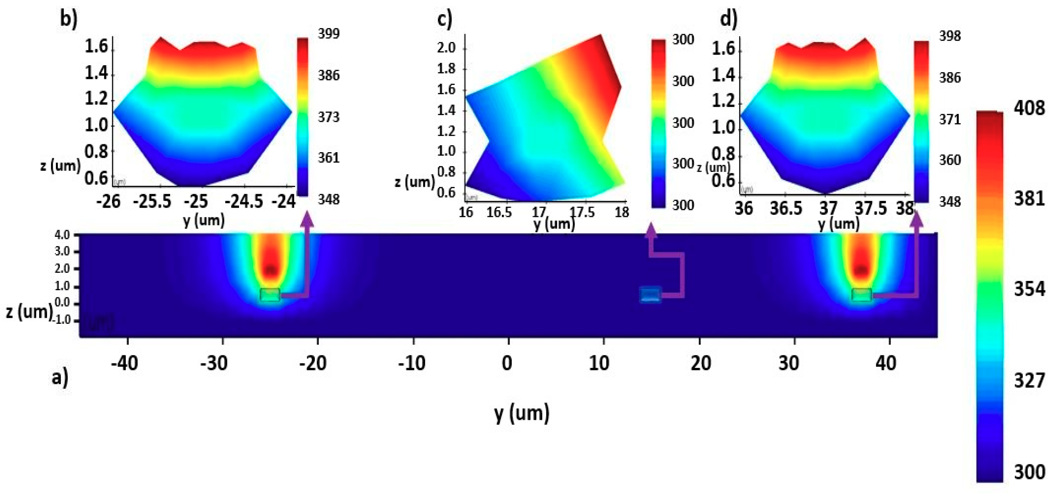
Figure 3a shows the temperature profile around the simulation region, and the temperature varies from 300 to 408 K for an input heater power of 30 mW to each heater.
Figure 3b, d illustrates the temperature profile around the lower arm of the MZI waveguide region and the racetrack resonator waveguide region, respectively. As expected, the temperature profile around the two heaters is almost identical and the thermal heating to the waveguides beneath the heaters can be clearly seen. On the other hand,
Figure 3c illustrates the temperature profile around the upper arm of the MZI waveguide region, where the temperature remains unchanged. This result implies that the heating in this structure is very localized, and no thermal crosstalk happens. In our design, thermal crosstalk is avoided by keeping a safe spacing between the two arms of the MZI waveguides.
To characterize the optical response, including the changes in the effective refractive index and phase as a function of the input heater power, the temperature map from the previous heat transport simulation needs to be imported into the finite difference eigenmode (FDE) solver of MODE Solutions. An index perturbation grid attribute is used to convert the temperature map into a change in refractive index of the material based on a user-specified thermal-optic coefficient. In the simulation, the thermal coefficients, (dn/dT), of 1.855 × 10
−4 and 1.317 × 10
−5 (K
−1) are used for silicon and silicon dioxide, respectively [
40]. The temperature data files are loaded into the temperature grid attribute of the Lumerical MODE Solution FDE solver to calculate the effective refractive index n
eff and the change in effective refractive index Δn
eff of the TE mode for different input powers of the heaters.
Figure 4a shows the change in the effective index for the racetrack waveguide and lower waveguide of the MZI. The phase shift in
can be obtained with less than 30 mW of heating power.
Figure 4b shows that the effective index change of the upper MZI waveguide (w/o heater) is three orders of magnitude smaller than that of the heated waveguide. Therefore, the heating power that comes from the two heaters does not affect the waveguide of the upper arm of the MZI. That is, no thermal crosstalk occurs in our design. The change in the effective refractive index for the upper arm racetrack waveguide and lower arm of the balanced Mach–Zehnder interferometer (BMZI) waveguide as a function of the input power of the heater is shown in
Figure 4a, and its accuracy level of the change in refractive index is within six decimal digits.
3.2. Integrated ODL Simulation Results
The Lumerical INTERCONNECT [
39] is used to model the integrated ODL of which the functional blocks are shown in
Figure 5. It is constructed with three MODE waveguides, two thermal modulators, two 3 dB couplers, two DC source components, and an optical network analyzer. In each component block, we import the exact file that comes from the previous MODE simulation. The waveguide and modulator properties are imported from data saved from MODE simulations. Data of the upper modulator modeling the index perturbation due to Heater 1 can be loaded into “Optical Modulator 1,” and data of the lower modulator modeling index perturbation due to Heater 2 can be loaded into “Optical Modulator 2.” The response of the devices was measured by means of the Optical Network Analyzer that allows the power transmission spectrum and group delay spectrum to be characterized.
Figure 6a depicts the group delay, power transmission, and wavelength at the resonant condition as a function of the input power of Heater 2 when the input power of Heater 1 is fixed at 0 mW. It corresponds to the case where only the coupling coefficient of the ODL is tuned. By tuning the input power of Heater 2 from 0 to 8 mW, the group delay, measured at the resonant peak, varies from 17.81 to 150.07 ps, while the corresponding power transmission efficiency, measured at the transmission dip in the spectrum, can be kept above 80% (<1 dB loss) over the tuning range. However, the peak wavelength varies from 1550.74 to 1550.86 nm during tuning. That is, the wavelength drifts at a rate of 0.015 nm/mW with respect to the power of Heater 2. This wavelength drift will result in a change in the group delay for a fixed wavelength and alter the tuning curve. Similarly,
Figure 6b shows the results for tuning the racetrack loop phase with Heater 1 by fixing the input power of Heater 2 at 0 mW. The peak group delay and power transmission are almost constant during Heater 1 tuning, but the wavelength varies linearly with a slope of 0.03 nm/mW. Thus, Heater 1 can be used to correct the resonant wavelength without affecting the group delay and power transmission.
Figure 7 shows contour plots of the wavelength and maximum (peak) group delay of the proposed ODL as a function of the input power of the two heaters. The contour plots will be used to illustrate how to tune the group delay and keep the peak wavelength intact.
Figure 7a shows the tuning of the peak wavelength versus the power to Heater 1 and 2, as indicated by the red arrow in
Figure 7a. This figure shows only one of the peaks among the multiple peaks caused by the ring resonance.
Figure 7b shows that the peak group delay can be continuously tuned by simply changing the input power to Heater 2 while it remains unchanged in tuning Heater 1. From
Figure 6, the wavelength drift rate is different for tuning Heater 2 and Heater 1. Moreover, the wavelength shifts to the same direction (longer wavelength) for tuning both heaters. To stabilize the wavelength in tuning the group delay, the two heaters need to be operated at the push–pull mode. That is, the heater power to Heater 1 must be decreased when the power to heater 2 increases. As indicated by the orange arrows in
Figure 7a, b as an example, the input power of Heater 2 is increased to increase the group delay; then, the input power to Heater 1 needs to be decreased to maintain the same peak wavelength.
The dashed blue line in
Figure 7a indicates the data points with the same resonant wavelength during the push–pull mode, i.e., 1550.89 nm.
Figure 8a shows the tuning spectrum for the push–pull operation. As the wavelength drift rate for tuning Heater 1 is about double that for tuning Heater 2, the input power for Heater 2 and Heater 1 is of a step of 2 and 1 mW, respectively, for the spectra shown in
Figure 8a. The resonant wavelength remains fixed during group delay tuning.
Figure 8b summarizes the maximal group delay, power transmission, and wavelength by tuning the two heaters together at the push–pull mode. As shown in
Figure 8b, the tuning of the input power of Heater 2, from 0 to 8 mW, causes the maximal group delay to vary from 17.81 to 150.81 ps with a similar power transmission change from 97.57% to 81.17% while the wavelength remains constant.
Figure 9 and
Figure 10 show that the group delay can be tuned over one free spectral range (FSR) by using <30 mW of the Heater 1 power when the input power of Heater 2 is 0 to 8 mW for different group delays. Due to the periodic delay-time characteristics of the ring resonance,
Figure 9 and
Figure 10 indicate that the proposed tunable delay lines can be tuned to track the wavelength of the input light sources over a wide wavelength range and provide the needed group delay.


