Synthesis, Structure and Photoluminescence Properties of 2D Organic–Inorganic Hybrid Perovskites

Abstract
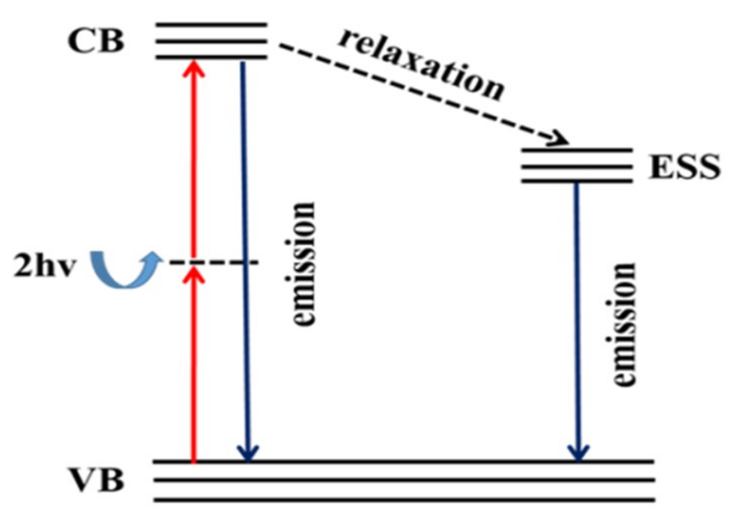
1. Introduction
2. Experiment
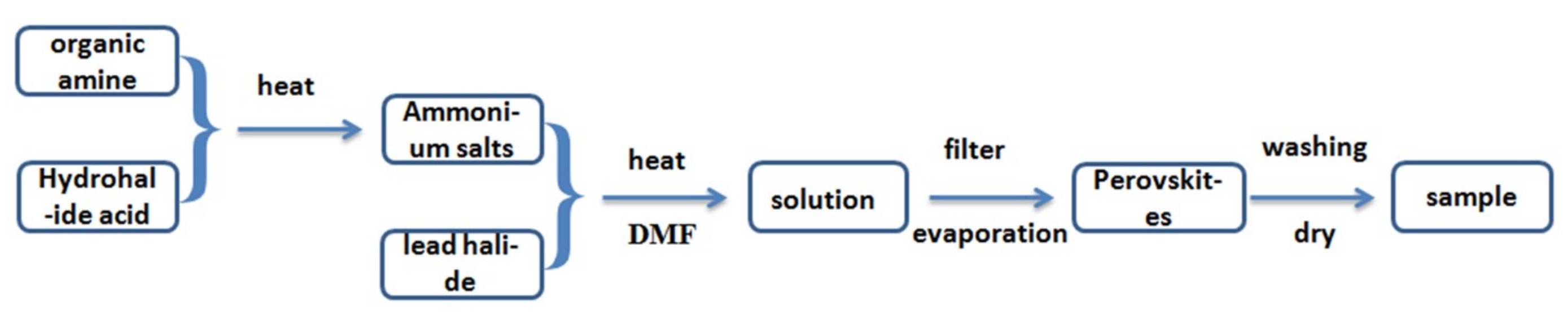
2.1. Synthesis of Organic Ammonium Salts
2.2. Synthesis of Perovskite Crystals
2.3. Synthesis of Perovskitenanosheet
2.4. Characterization
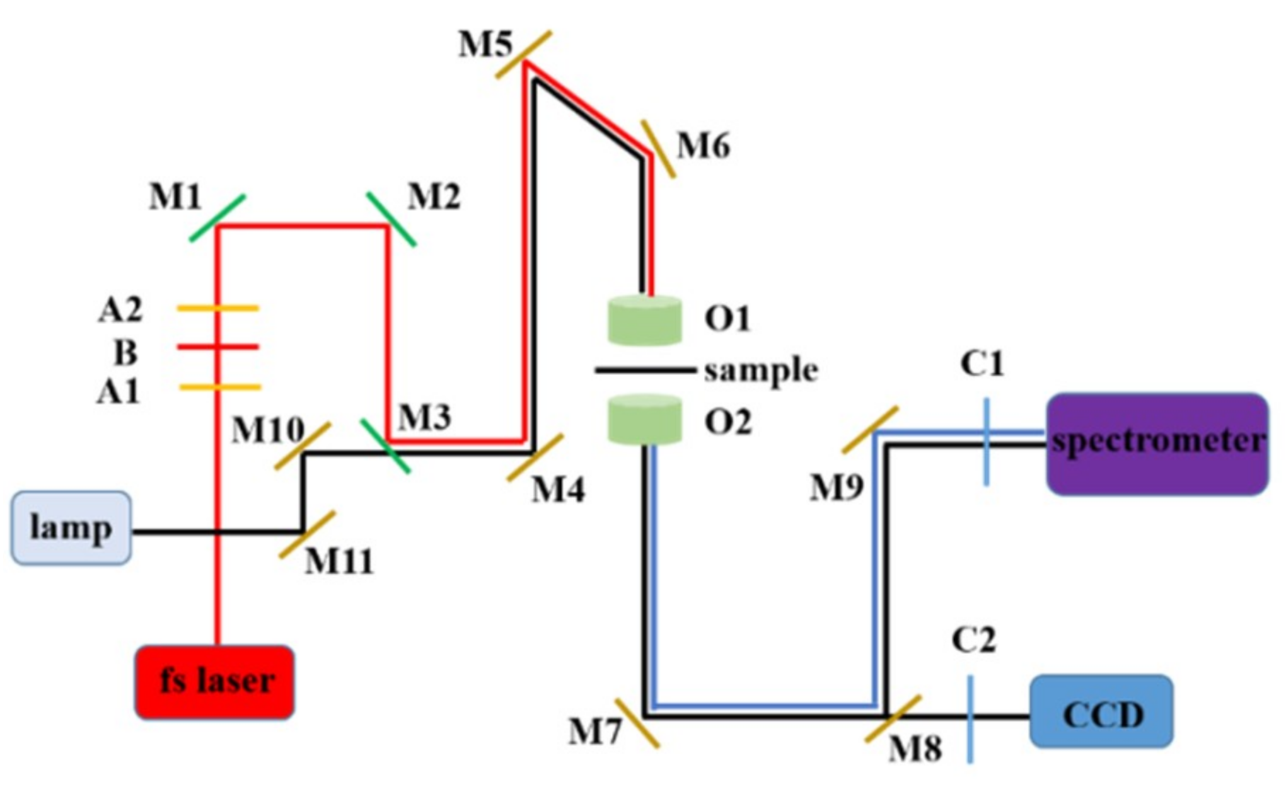
2.5. The Experimental Optical Path
3. Results and Discussion
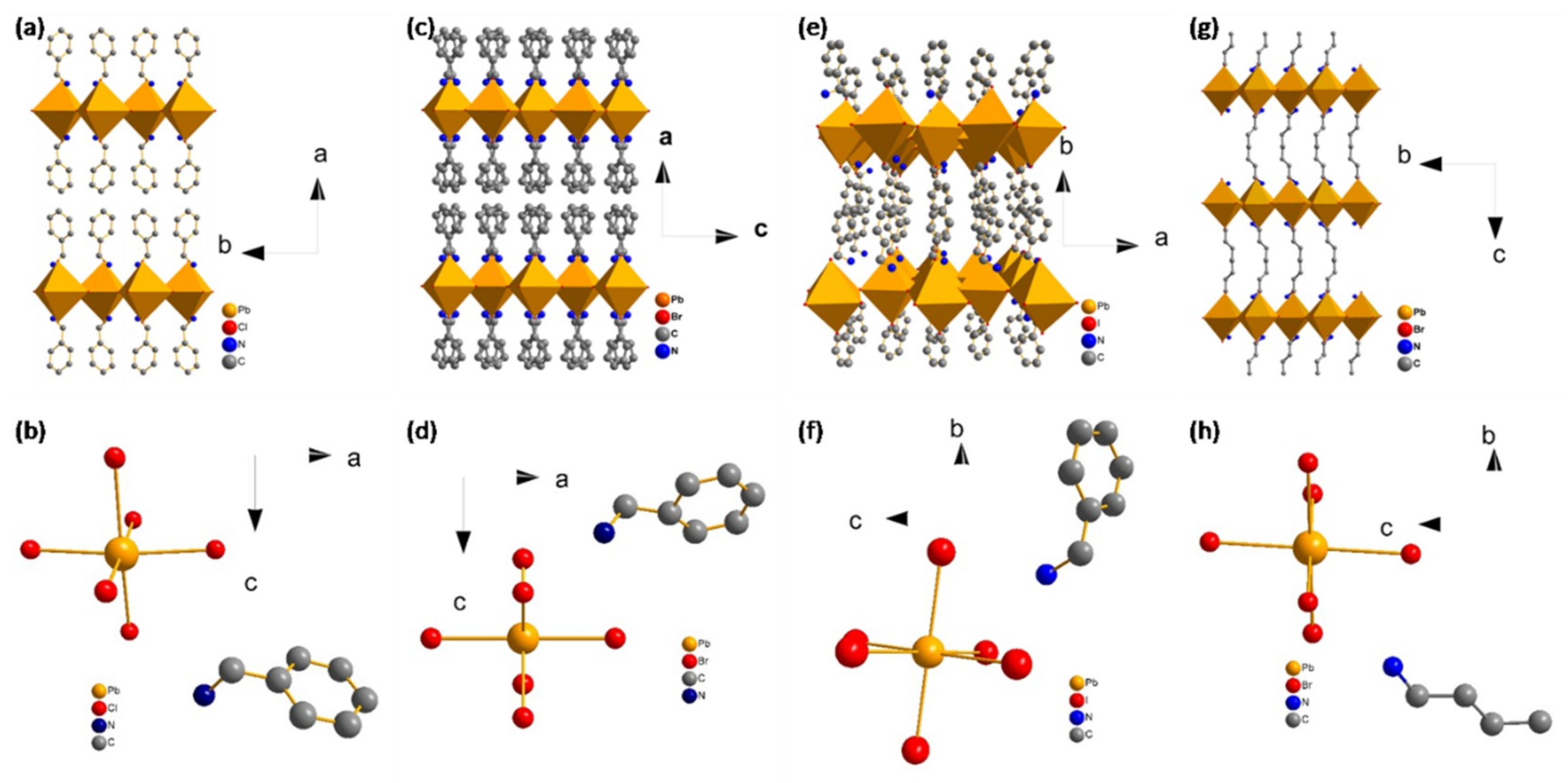
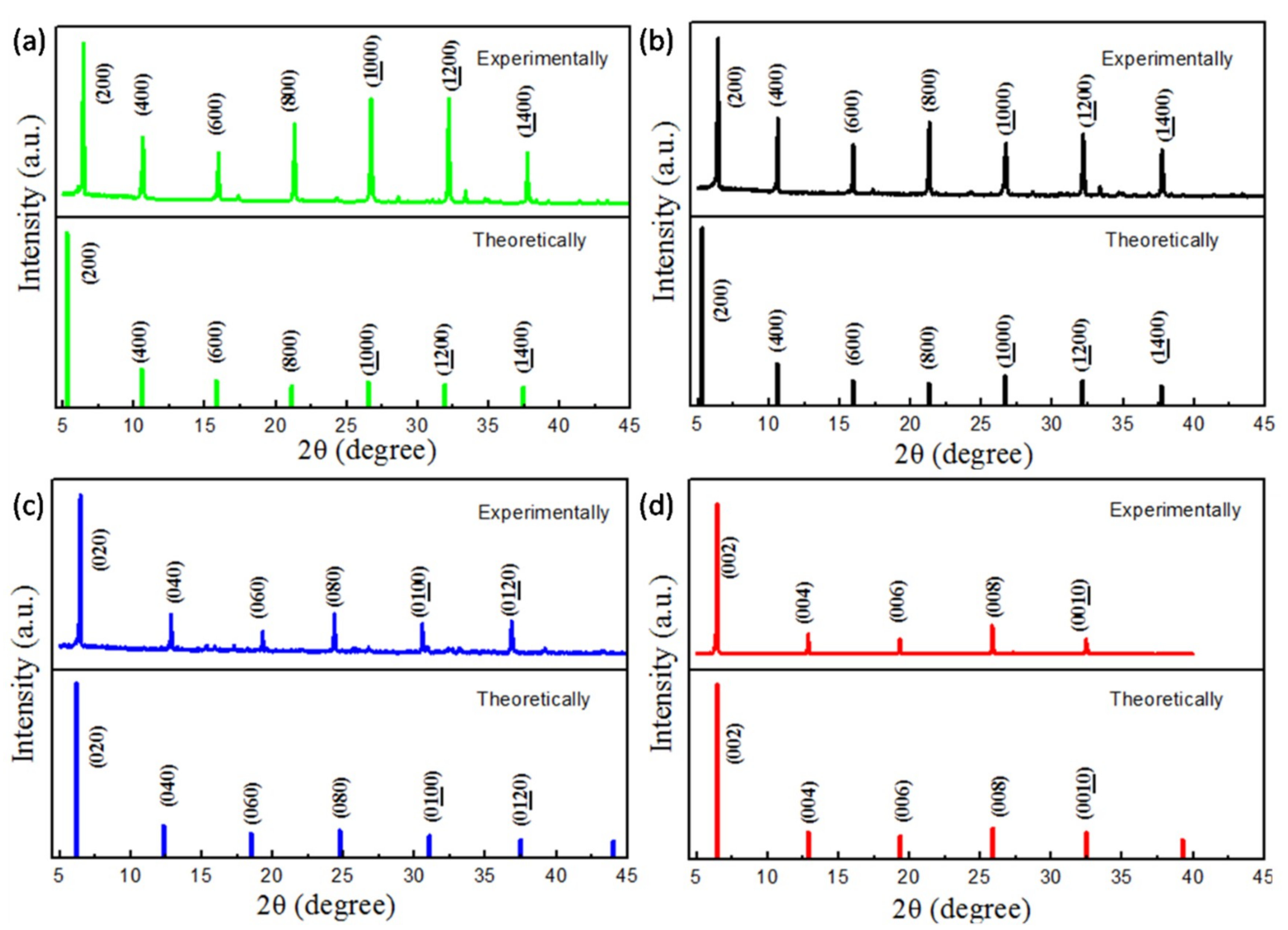
3.1. Structure Characterization
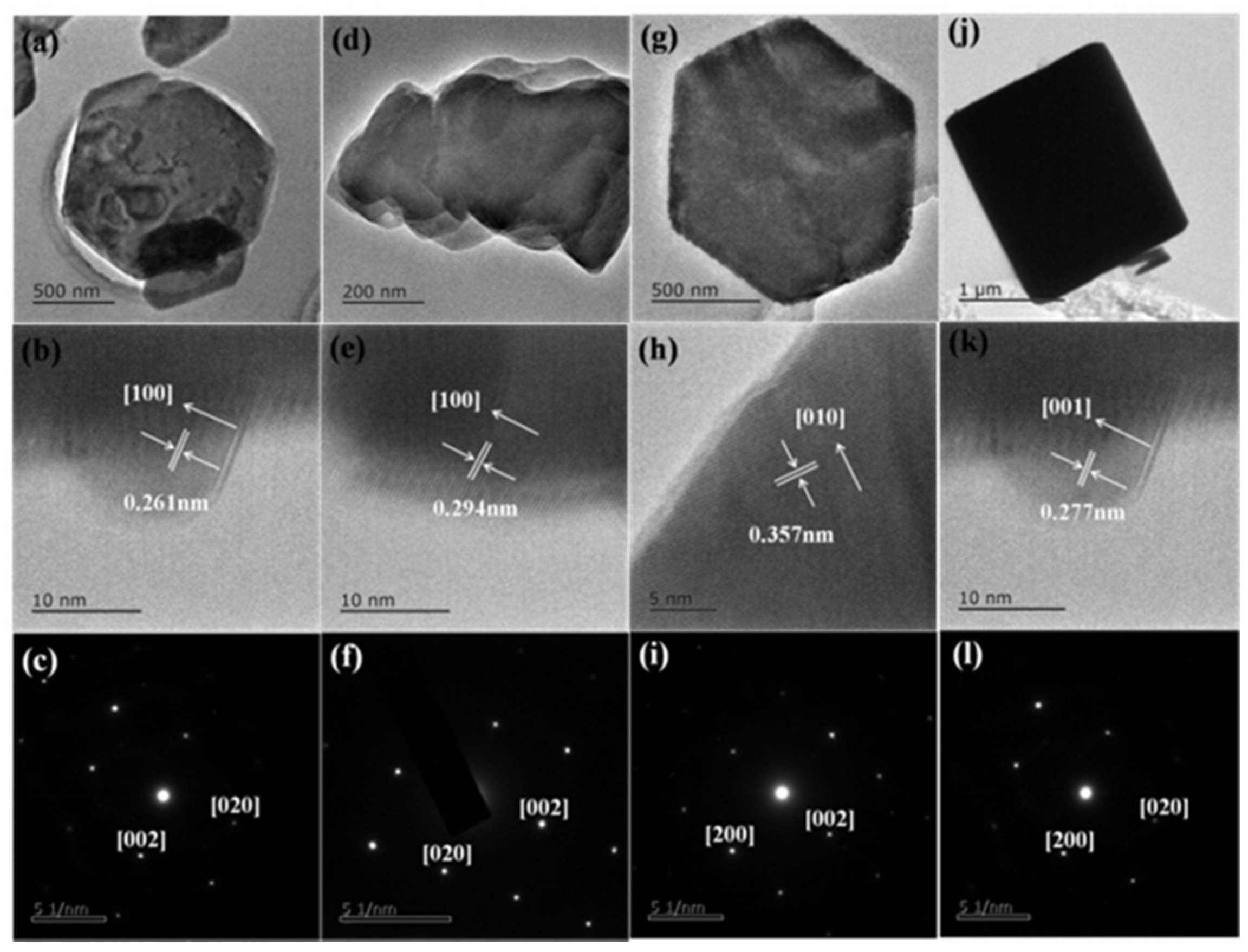
3.2. Morphology Characterization
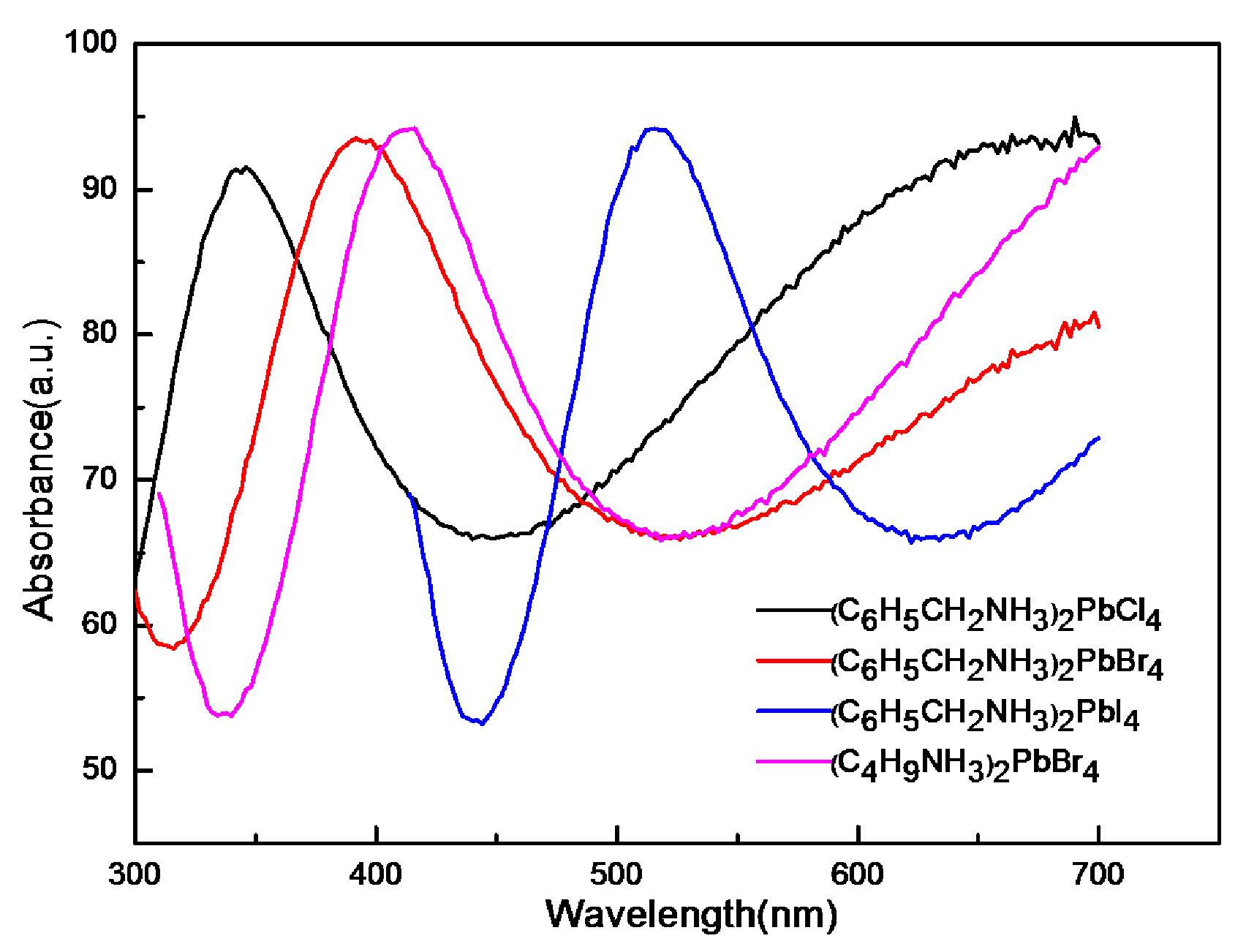
3.3. Absorption Spectrum
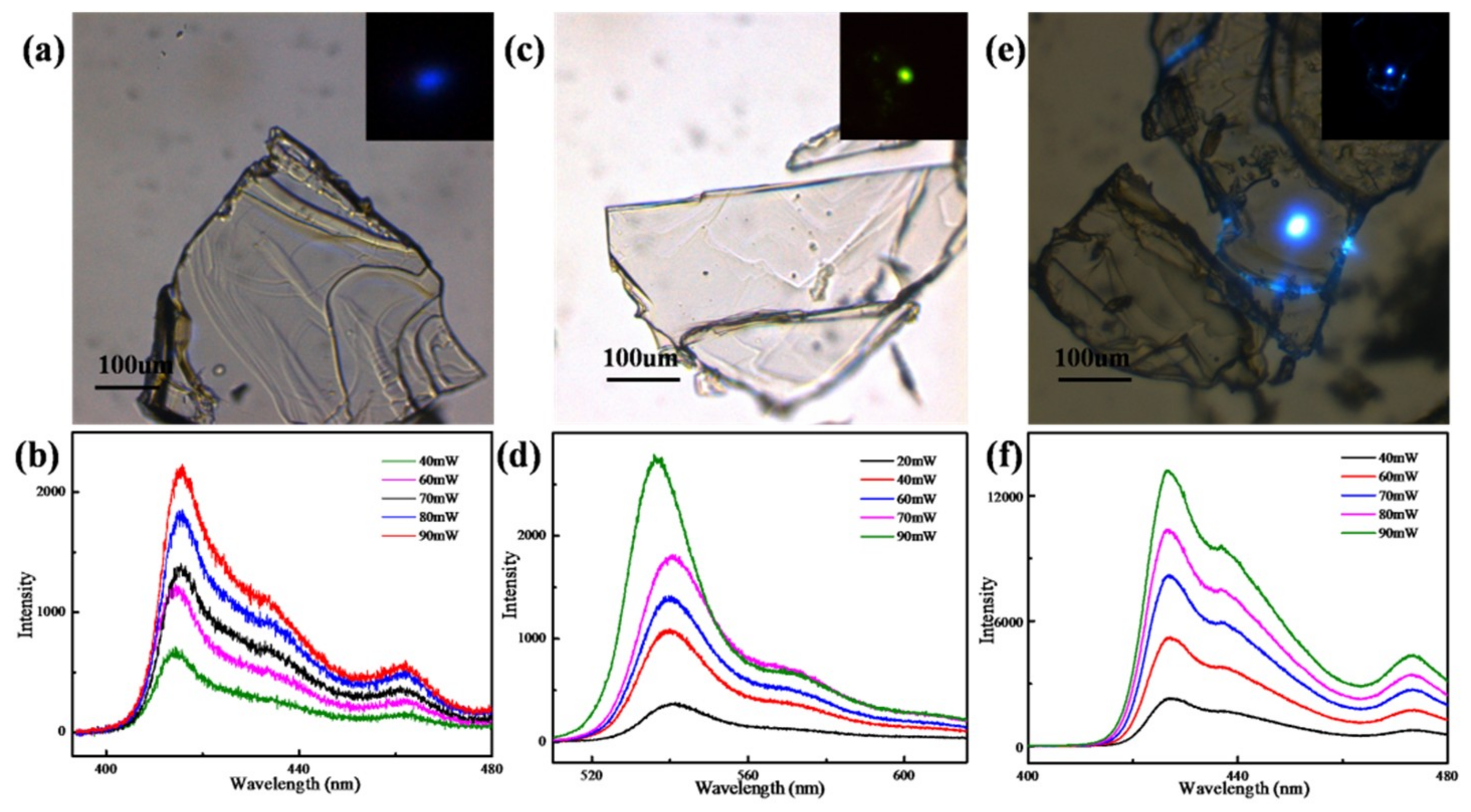
3.4. The Laser Power Effect on the PL Intensity
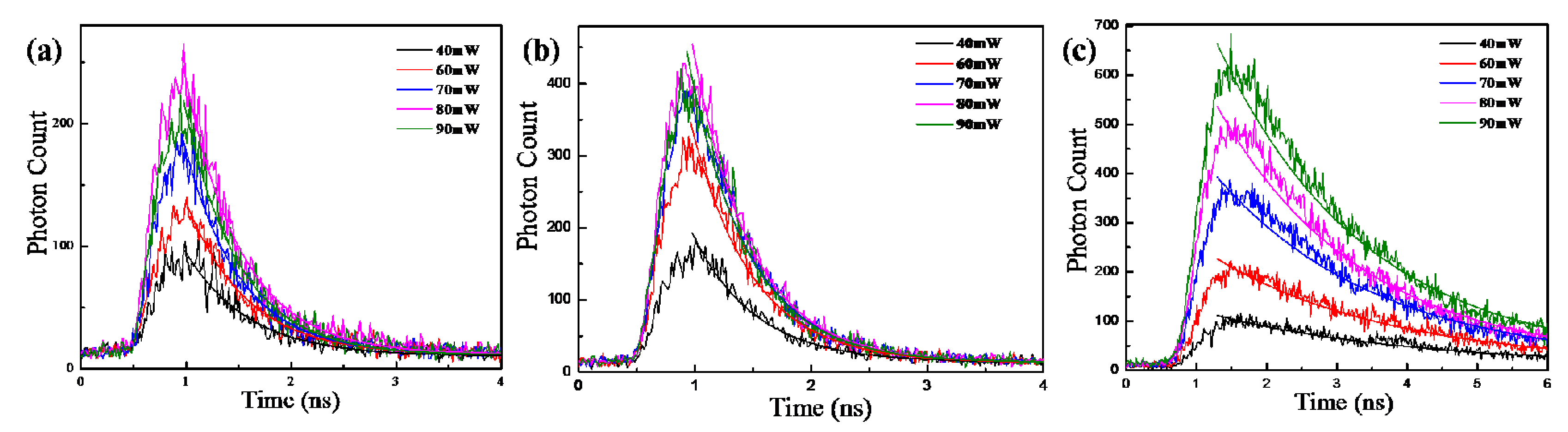
3.5. The Laser Power Effect on the PL Lifetime
4. Conclusions
Author Contributions
Funding
Acknowledgments
Conflicts of Interest
References
- Saparov, B.; Mitzi, D.B. Organic Inorganic Perovskites: Structural Versatility for Functional Materials Design. Chem. Rev. 2016, 116, 4558–4596. [Google Scholar] [CrossRef]
- Li, W.; Wang, Z.; Deschler, F.; Gao, S.; Friend, R.H.; Cheetham, A.K. Chemically diverse and multifunctional hybrid organic inorganic perovskites. Nat. Rev. Mater. 2017, 2, 16099. [Google Scholar] [CrossRef]
- Shi, E.; Gao, Y.; Finkenauer, B.P.; Akriti Coffey, A.H.; Dou, L. Two-dimensional halide perovskite nanomaterials and heterostructures. Chem. Soc. Rev. 2018, 47, 6046–6072. [Google Scholar] [CrossRef] [PubMed]
- Tian, Y.; Merdasa, A.; Unger, E.; Abdellah, M.; Zheng, K.; Mckibbin, S.; Mikkelsen, A.; Pullerits, T.; Yartsev, A.; Sundstrom, V.; et al. Enhanced Organo-Metal Halide Perovskite Photoluminescence from Nanosized Defect-Free Crystallites and Emitting Sites. J. Phys. Chem. Lett. 2015, 6, 4171–4177. [Google Scholar] [CrossRef] [PubMed]
- Kim, T.W.; Uchida, S.; Matsushita, T.; Cojocaru, L.; Jono, R.; Kimura, K.; Matsubara, D.; Shirai, M.; Mastsumoto, H.; Kondo, T.; et al. Self-Organized Superlattice and Phase Coexistence inside Thin Film Organometal Halide Perovskite. Adv. Mater. 2018, 30, 1705230. [Google Scholar] [CrossRef]
- Dong, L.Y.; Sun, S.J.; Deng, Z.Y.; Li, W.; Wei, F.X.; Qi, Y.J.; Li, Y.C.; Li, X.D.; Lu, P.X.; Ramamurty, U. Elastic properties and thermal expansion of lead-free halide double perovskite Cs2AgBiBr6. Comput. Mater. Sci. 2018, 141, 49–58. [Google Scholar]
- Zhang, L.; Liang, W.Z. How the Structures and Properties of Two-Dimensional Layered Perovskites MAPbI3 and CsPbI3 Vary with the Number of Layers. J. Phys. Chem. Lett. 2017, 8, 1517–1523. [Google Scholar] [CrossRef]
- Mitzi, D.B. Templating and structural engineering in organic–inorganic perovskites. J. Chem. Soc. Dalton Trans. 2001, 1, 1–12. [Google Scholar] [CrossRef]
- Hong, X.; Ishihara, T.; Nurmikko, A.V. Photoconductivity and electroluminescence in lead iodide based natural quantum well structures. Solid State Commun. 1992, 84, 657–661. [Google Scholar] [CrossRef]
- Mitzi, D.B. ChemInform Abstract: Synthesis, Structure, and Properties of Organic-Inorganic Perovskites and Related Materials. ChemInform 2010, 30. [Google Scholar] [CrossRef]
- Umebayashi, T.; Asai, K.; Kondo, T.; Nakao, A. Electronic structures of lead iodide based low-dimensional crystals. Phys. Rev. B 2003, 67, 155405. [Google Scholar] [CrossRef]
- Yuan, Z.; Shu, Y.; Tian, Y.; Xin, Y.; Ma, B.W. A facile one-pot synthesis of deep blue luminescent lead bromide perovskite microdisks. Chem. Commun. 2015, 51, 16385–16388. [Google Scholar] [CrossRef] [PubMed]
- Yaffe, O.; Chernikov, A.; Norman, Z.M.; Zhong, Y.; Velauthapillai, A.; Zande, A.; Owen, J.S.; Heinz, T.F. Excitons in ultrathin organic-inorganic perovskite crystals. Phys. Rev. B 2015, 92, 045414. [Google Scholar] [CrossRef]
- Brenner, T.M.; Egger, D.A.; Kronik, L.; Hodes, G.; Cahen, D. Hybrid organic—Inorganic perovskites: Low-cost semiconductors with intriguing charge-transport properties. Nat. Rev. Mater. 2016, 1, 15007. [Google Scholar] [CrossRef]
- Han, X.B.; Wang, K.; Long, H.; Hu, H.B.; Chen, J.W.; Wang, B.; Lu, P.X. Highly sensitive detection of the lattice distortion in single bent ZnO nanowires by second harmonic generation microscopy. ACS Photonics 2016, 3, 1308–1314. [Google Scholar] [CrossRef]
- Zhang, S.J.; Audebert, P.; Wei, Y.; AIC, A.; Lanty, G.; Brehier, A.; Galmiche, L.; Clavier, G.; Boissiere, C.; Lauret, J.S.; et al. Preparations and Characterizations of Luminescent Two Dimensional Organic-inorganic Perovskite Semiconductors. Materials 2010, 3, 3385–3406. [Google Scholar] [CrossRef]
- Kawano, N.; Koshimizu, M.; Sun, Y.; Yahaba, N.; Fujimoto, Y.; Yanagida, T.; Asai, K. Effects of Organic Moieties on Luminescence Properties of Organic–Inorganic Layered Perovskite-Type Compounds. J. Phys. Chem. C 2014, 118, 9101–9106. [Google Scholar] [CrossRef]
- Qin, P.L.; Lei, H.W.; Zheng, X.L.; Liu, Q.; Tao, H.; Yang, G.; Ke, W.J.; Xiong, L.B.; Qin, M.C.; Zhao, X.Z.; et al. Copper-Doped Chromium Oxide Hole-Transporting Layer for Perovskite Solar Cells: Interface Engineering and Performance Improvement. Adv. Mater. Interfaces 2016, 3, 1500799. [Google Scholar] [CrossRef]
- Deng, Q.R.; Li, Y.Q.; Chen, L.A.; Wang, S.G.; Wang, G.M.; Sheng, Y.L.; Shao, G.S. The effects of electron and hole transport layer with the electrode work function on perovskite solar cells. Mod. Phys. Lett. B 2016, 30, 1650341. [Google Scholar] [CrossRef]
- Qin, P.L.; He, Q.; Dan, O.Y.; Fang, G.J.; Choy, W.C.H.; Li, G. Transition metal oxides as hole-transporting materials in organic semiconductor and hybrid perovskite based solar cells. Sci. China Chem. 2017, 60, 472–489. [Google Scholar] [CrossRef]
- Qin, X.; Dong, H.L.; Hu, W.P. Green light-emitting diode from bromine based organic inorganic halide perovskite. Sci. China Mater. 2015, 58, 186–191. [Google Scholar] [CrossRef]
- Tan, Z.K.; Moghaddam, R.S.; Lai, M.L.; Docampo, P.; Higler, R.; Deschler, F.; Price, M.; Sadhanala, A.; Pazos, L.M.; Credgington, D.; et al. Bright light emitting diodes based on organometal halide perovskite. Nat. Nanotechnol. 2014, 9, 687–692. [Google Scholar] [CrossRef] [PubMed]
- Xu, L.T.; Li, F.; Wei, L.; Zhou, J.X.; Liu, S. Design of Surface Plasmon Nanolaser Based on MoS2. Appl. Sci. 2018, 8, 2110. [Google Scholar] [CrossRef]
- Xu, L.T.; Li, F.; Liu, S.; Yao, F.Q.; Liu, Y.H. Low Threshold Plasmonic Nanolaser Based on Graphene. Appl. Sci. 2018, 8, 2186. [Google Scholar] [CrossRef]
- Xu, L.T.; Li, F.; Liu, Y.; Yao, F.Q.; Liu, S. Surface Plasmon Nanolaser: Principle, Structure, Characteristics and Applications. Appl. Sci. 2019, 9, 861. [Google Scholar] [CrossRef]
- Stoumpos, C.C.; Malliakas, C.D.; Peters, J.; Liu, Z.F.; Sebastian, M.; Im, J.; Chasapis, T.; Wibowo, A.; Chung, D.Y.; Freeman, A.; et al. Crystal Growth of the Perovskite Semiconductor CsPbBr3: A New Material for High Energy Radiation Detection. Crys. Grow. Des. 2013, 13, 2722–2727. [Google Scholar] [CrossRef]
- Dou, L.; Yang, Y.M.; You, J.; Hong, Z.R.; Chang, W.H.; Li, G.; Yang, Y. Solution processed hybrid perovskite photodetectors with high detectivity. Nat. Commun. 2014, 5, 5404. [Google Scholar] [CrossRef]
- Kojima, A.; Teshima, K.; Shirai, Y.; Miyasaka, T. Organometal Halide Perovskites as Visible Light Sensitizers for Photovoltaic Cells. J. Am. Chem. Soc. 2009, 131, 6050–6051. [Google Scholar] [CrossRef]
- Kawano, N.; Koshimizu, M.; Asai, K. The Effect of Wannier and Frenkel Exciton Resonance on the Luminescence Properties of Organic Inorganic Layered Perovskite-Type Compounds. J. Am. Chem. Soc. 2012, 116, 22992–22995. [Google Scholar] [CrossRef]
- Slavney, A.H.; Hu, T.; Lindenberg, A.M.; Karunadasa, H.I. A Bismuth-Halide Double Perovskite with Long Carrier Recombination Lifetime for Photovoltaic Applications. J. Am. Chem. Soc. 2016, 138, 2138–2141. [Google Scholar] [CrossRef]
- Hu, X.; Zhou, H.; Jiang, Z.; Wang, X.; Yuan, S.P.; Lan, J.Y.; Fu, Y.P.; Zhang, X.H.; Zheng, W.H.; Wang, X.X.; et al. Direct Vapor Growth of Perovskite CsPbBr3 Nanoplate Electroluminescence Devices. ACS Nano. 2017, 11, 9869–9876. [Google Scholar] [CrossRef] [PubMed]
- Chen, J.; Gan, L.; Zhuge, F.; Li, H.; Song, J.; Zeng, H.; Zhai, T. A Ternary Solvent Method for Large Sized Two Dimensional Perovskites. Angew. Chem. Int. Ed. 2017, 56, 2390–2394. [Google Scholar] [CrossRef] [PubMed]
- Luo, D.; Yang, W.; Wang, Z.; Wang, Z.P.; Sadhanala, A.; Hu, Q.; Su, R.; Shivanna, R.; Trindade, G.F.; Watts, J.F.; et al. Enhanced photovoltage for inverted planar heterojunction perovskite solar cells. Science 2018, 360, 1442–1446. [Google Scholar] [CrossRef]
- Chen, C.; He, Y.C.; Du, Z.P.; Yuan, H.; Wu, Y.X. Preparation and properties of perovskite-type La0.5Pb0.5MnO3 by stearic acid method. Mater. Lett. 2013, 110, 264–266. [Google Scholar] [CrossRef]
- Liao, W.Q.; Zhang, Y.; Hu, C.L.; Mao, J.G.; Ye, H.Y.; Li, P.F.; Huang, S.D.; Xiong, R.G. A lead halide perovskite molecular ferroelectric semiconductor. Nat. Commun. 2015, 6, 7338. [Google Scholar] [CrossRef] [PubMed]
- Papavassiliou, G.C.; Mousdis, G.A.; Raptopoulou, C.P. Preparation and characterization of perovskite (C6H5CH2NH3)2PbI4, [C6H5C2H4SC(NH2)2]3PbI5 and (C10H7CH2NH3)2PbI3 organic inorganic hybrid compounds. Z. Nat. B 1999, 54, 1405–1409. [Google Scholar]
- Dou, L.; Wong, A.B.; Yu, Y.; Lai, M.L.; Kornienko, N.; Eaton, S.W.; Fu, A.; Bischak, C.G.; Ma, J.; Ding, T.; et al. Atomically thin twodimensionalorganicinorganic hybrid perovskites. Science 2015, 349, 1518–1521. [Google Scholar] [CrossRef]
- Xu, W.; Mcleod, J.A.; Yang, Y.; Wang, Y.; Wu, Z.W.; Bai, S.; Yuan, Z.C.; Song, T.; Wang, Y.S.; Si, J.J.; et al. Iodomethane Mediated Organometal Halide Perovskite with Record Photoluminescence Lifetime. ACS Appl. Mater. Interfaces 2016, 8, 23181. [Google Scholar] [CrossRef]
- Li, F.; He, Z.C.; Li, M.Y.; Zhang, J.P.; Han, J.B.; Lu, P.X. Photoinduced energy transfer in a CdTe quantum dot copper phthalocyanine system via two photon excitation. Mater. Lett. 2014, 132, 263–266. [Google Scholar] [CrossRef]
- Li, F.; Lu, P.X.; Long, H.; Yang, G.; Li, Y.H.; Zheng, Q.G. Nonlinear absorption in CuPc-doped PMMA thin film in the femtosecond regime: Experimental and theoretical studies. Opt. Express 2008, 16, 14571–14581. [Google Scholar] [CrossRef]
- Li, F.; He, Z.; Li, M.; Lu, P. Three-photon absorption of copper phthalocyanine solution by femtosecond Z-scan technique. Mater. Lett. 2013, 111, 81–84. [Google Scholar] [CrossRef]
- Li, F.; Li, X. Theoretical investigation on nonlinear absorption of multilevel organic molecular system in ns, ps and fs regime. Opt. Commun. 2012, 285, 5217–5222. [Google Scholar] [CrossRef]
- Liu, W.W.; Li, X.H.; Song, Y.L.; Zhang, C.; Han, X.B.; Long, H.; Wang, B.; Wang, K.; Lu, P.X. Cooperative Enhancement of Two Photon Absorption Induced Photoluminescence from a 2D Perovskite Microsphere Hybrid Dielectric Structure. Adv. Funct. Mater. 2018, 28, 1707550. [Google Scholar] [CrossRef]


| Unit: nm | ||||
|---|---|---|---|---|
| (C6H5CH2NH3)2PbCl4 | (C6H5CH2NH3)2PbBr4 | (C6H5CH2NH3)2PbI4 | (C4H9NH3)2PbBr4 | |
| C1–C2 | 0.1463 | 0.1494 | 0.1481 | 0.1429 |
| C2–C3 | 0.1392 | 0.1385 | 0.1363 | 0.1482 |
| C3–C4 | 0.135 | 0.1386 | 0.1372 | 0.1438 |
| C4–C5 | 0.1369 | 0.1384 | 0.1342 | 0.1461 |
| C5–C6 | 0.1322 | 0.1389 | 0.134 | - |
| C6–C7 | 0.1412 | 0.1387 | 0.1358 | - |
| C7–C2 | 0.1371 | 0.1387 | 0.1367 | - |
| C1–N | 0.1521 | 0.1447 | 0.1507 | - |
| Pb–X1 | 0.2877 | 0.2998 | 0.3224 | 0.3005 |
| Pb–X2 | 0.2841 | 0.2979 | 0.3203 | 0.2938 |
| Pb–X3 | 0.2886 | 0.2982 | 0.3198 | 0.2973 |
| Formula | (C7H10N)2PbCl4 | (C7H10N)2PbBr4 | (C7H10N)2PbI4 | (C4H12N)2PbBr4 |
|---|---|---|---|---|
| Weight | 565 | 743 | 931 | 675 |
| Temperature (K) | 293 | 293 | 293 | 323 |
| Crystal system | orthorhombic | Orthorhombic | orthorhombic | orthorhombic |
| Space group | Cmc21 | Cmca | Pbca | Pbca |
| a (A) | 33.619 | 33.394 | 8.689 | 8.22 |
| b (A) | 7.819 | 8.153 | 28.78 | 8.33 |
| c (A) | 7.728 | 8.131 | 9.162 | 27.62 |
| V (A3) | 2034 | 2214 | 2291 | 1895 |
| Z | 4 | 4 | 4 | 4 |
| ρ (g/cm3) | 1.846 | 2.230 | 2.699 | 2.370 |
| μ (mm−1) | 8.814 | 14.836 | 17.34 | 17.30 |
© 2019 by the authors. Licensee MDPI, Basel, Switzerland. This article is an open access article distributed under the terms and conditions of the Creative Commons Attribution (CC BY) license (http://creativecommons.org/licenses/by/4.0/).
Share and Cite
Liu, Y.; Li, F.; Yao, F.; He, Z.; Liu, S.; Xu, L.; Han, X.; Wang, K. Synthesis, Structure and Photoluminescence Properties of 2D Organic–Inorganic Hybrid Perovskites. Appl. Sci. 2019, 9, 5211. https://doi.org/10.3390/app9235211
Liu Y, Li F, Yao F, He Z, Liu S, Xu L, Han X, Wang K. Synthesis, Structure and Photoluminescence Properties of 2D Organic–Inorganic Hybrid Perovskites. Applied Sciences. 2019; 9(23):5211. https://doi.org/10.3390/app9235211
Chicago/Turabian StyleLiu, Yahui, Fang Li, Fuqiang Yao, Zhicong He, Shuai Liu, Litu Xu, Xiaobo Han, and Kai Wang. 2019. "Synthesis, Structure and Photoluminescence Properties of 2D Organic–Inorganic Hybrid Perovskites" Applied Sciences 9, no. 23: 5211. https://doi.org/10.3390/app9235211
APA StyleLiu, Y., Li, F., Yao, F., He, Z., Liu, S., Xu, L., Han, X., & Wang, K. (2019). Synthesis, Structure and Photoluminescence Properties of 2D Organic–Inorganic Hybrid Perovskites. Applied Sciences, 9(23), 5211. https://doi.org/10.3390/app9235211