1. Introduction
Surface-enhanced Raman scattering (SERS) is a sophisticated analytical technique to detect minute amounts of target analyte, even down to a single molecule, by providing molecule-specific vibrational spectra. The SERS phenomenon is attributed to two effects: Electromagnetic and chemical enhancement mechanisms. Electromagnetic enhancement is due to the enhanced electromagnetic fields localized on or in the immediate vicinity of a nanostructured metallic surface generated by the excitation of localized surface plasmons. On the other hand, chemical enhancement results from the charge transfer between a metal substrate and the adsorbed molecule onto its surface [
1,
2,
3]. Moreover, SERS enhancement relies on the spatially localized regions of intense local electromagnetic field “hot spots”, which are generated at the junctions or gaps of two or more SERS-active substrates, hence providing a huge SERS signal enhancement [
4,
5]. Raman signal enhanced by the surface plasmon resonance was originally observed from a metal colloidal substrate, such as silver (Ag) nanoparticles. Due to the unstable motion of solution-based colloidal metal nanoparticles, a planar substrate, such as Au-coated glass substrate, became a favorable and commercially available SERS substrate. However, the advantages of using metallic nanostructure still attract attention in SERS detecting with high sensitivity or selectivity.
PSi with high surface-to-volume ratio due to the open nanopores and Si nanostructure was first reported for use as SERS template for the deposition of metallic film by Chan et al. in 2003 [
6]. The metallic nanostructure layer on the PSi substrate was fabricated by immersing PSi into aqueous AgNO
3 solution to produce the nanocomposite SERS substrate, which amplified the Raman signal of R6G by ten orders of magnitude. Later on, Lin et al. the pioneer of fabricating and characterizing PSi, introduced a roughened Ag film-coated PSi (Ag–PSi) planar SERS-active substrate by immersion plating of Ag on PSi, where the roughened Ag film produced randomly spaced dendritic structure. The Ag–PSi was further pretreated with mineral acids (HCl or H
2SO
4) to minimize the background signals in the SERS spectrum [
7]. Different Ag immersion conditions generate different Ag nanostructure on PSi substrate and, consequently, contribute to different SERS amplification. For example, Giorgis et al. immersed PSi samples into AgNO
3 solution and a successive thermal annealing to create the Ag nanocrystallites, which consequently removed the background Raman noise and further enhanced Raman signal [
8]. A simple dipping of PSi into aqueous AgNO
3 solution is still the common and preferred way to fabricate Ag–PSi SERS-active substrates [
9,
10,
11,
12,
13].
Despite the simple and easy solution-based process of fabricating metallic nanostructure on PSi, the intensity fluctuation of SERS signal and irregular hot spot generation, due to the inhomogeneous metallic nanostructure [
14], have hindered the progress of using metallic film-coated nanostructure as a SERS substrate. In other words, it is difficult to get the quantitative value of Raman signal using these solution-processed SERS substrates. In addition, the generation of metallic nanostructures using solution processing in some instances requires additional reducing agent and extra chemical treatment. The reducing agent may bring more negative electric charges on a SERS substrate, where the negative charge could repulse the targeting molecules and further weaken the Raman signal. These problems could be prevented by utilizing physical vapor deposition of metallic nanofilm on nanostructured template [
15,
16]. Dridi et al. fabricated PSi-coated Au thin film SERS substrates by electrochemical anodization of the rough back side of the silicon wafer, followed by Au sputtering via PVD technique at room temperature. In addition, the thickness of Au film over etched PSi substrates was controlled by changing the deposition time from 10 to 30 s [
16]. On the other hand, Kaminska et al. prepared Au-capped PSi substrate by the same procedure of galvanostatic anodic etch on the smooth surface of the crystalline Si wafer to achieve a specific thickness PSi with appropriate porous nanostructure, followed by PVD-based Au sputtering to deposit Au film of variable thickness (10, 30, 50, 100, 200, and 300 nm) [
17]. However, in another study, Lee et al. theoretically and experimentally investigated the PSi SERS substrate consisting of sputtered Ag nanofilm with desired surface roughness and thickness by changing the deposited template [
18]. A PSi–Ag substrate using nanovoid template exhibited the highest SERS signal at the thickness of 20 nm, and the signal was decreased with increasing Ag film thickness. SERS intensity of 10 nm Ag film using a flat substrate as template was less sensitive compared to the same thickness of Ag film coated on nanovoid structure. Their theoretical studies thus provided useful understanding about the role of template with different surface morphology and metallic film thickness to fabricate more accurate, stable, and cost-effective SERS substrates [
18].
Herein this study, the Au nanofilm-coated PSi was investigated as a simple, robust, and cost-effective SERS substrate. Unlike the previously reported nanostructured template fabricated by the conventional lithographic process, in this study, a more cost-effective and less time consuming single step electrochemical etching process was followed to obtain PSi with nano-sized surface roughness. Moreover, the metallic film deposition over the PSi template was done by the sputtering technique, which aided in obtaining the homogeneous nanofilm rapidly with large scale. In addition, Au films of different thicknesses (5, 7, and 10 nm) were sputtered on PSi and flat Si surface to observe the contribution of Au nanocrystallites in the variable layer, as well as surface roughness in the SERS enhancement. SERS study of Si- or PSi-coated Au thin films was conducted by using R6G dye. PSi–Au thin film was proved as a better SERS substrate than Si–Au thin film, while PSi–Au thin film of 7 nm thickness exhibited the highest SERS activity of all the fabricated composites. Therefore, the facile and straightforward fabrication method led to achieve a robust and reproducible PSi–Au thin film SERS substrate, which would be beneficial to a wide range of sophisticated applications.
3. Results and Discussion
Freshly prepared PSi is metastable and reactive due to the presence of hydrogen-terminated Si–H
x (x = 1, 2, 3) on the external layer of the PSi, therefore vulnerable to react with the impurities present in the electrolytes used in etching process or from the air of the material storage environment [
21]. At ambient condition, the unstable Si–H
x undergoes spontaneous oxidation; hence, it is important to coat the PSi surface to improve its stability. In this study, Au nanofilm of different thicknesses were deposited on the PSi substrate by e-beam evaporation, in which the surface of the pores was coated by immediate electroless deposition of Au ions via simultaneous Au reduction and Si oxidation reactions. The surface roughness feature of the PSi provides a large number of nucleation sites due to the lower free energy for nucleation than the Si flat surface [
22]. Therefore, large numbers of Au nuclei are generated on the PSi surface, which consequently facilitate the formation of Au nanocrystallites on roughened PSi surface at a higher rate in comparison to the conventional flat Si surface. In addition, the edge of PSi induces a stronger electric field, resulting in a higher density of Au crystallites due to the edge specific surface defect that heightens the reactivity and stimulates the Au reduction [
23].
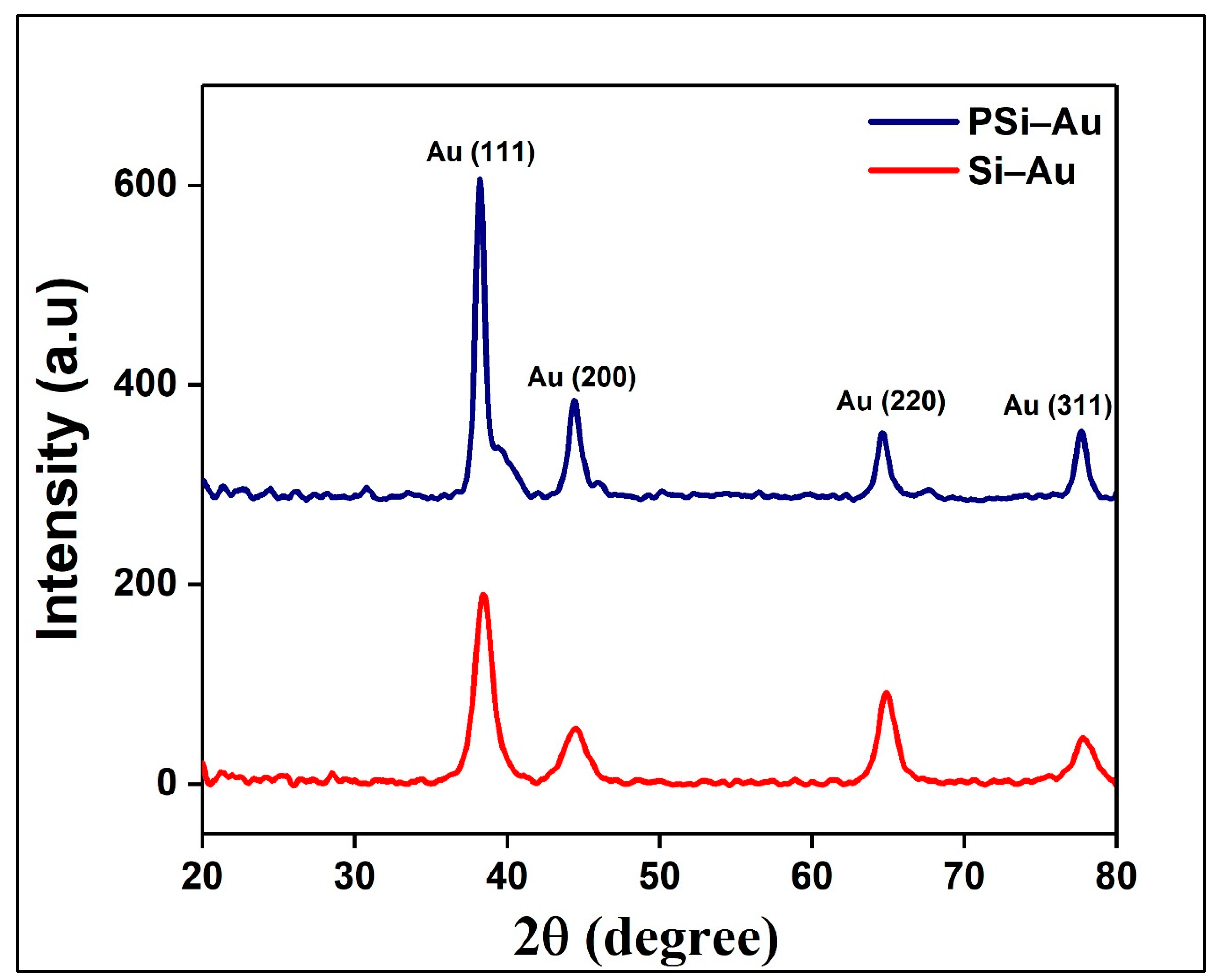
The fabricated Si–Au and PSi–Au SERS substrates were first investigated by XRD technique. XRD spectra of Si–Au sample produced four diffraction peaks at 2θ = 38.45°, 44.51°, 64.85°, and 77.75°, while PSi–Au sample also represented the four diffraction peaks at the same position with very little blue-shifting at 2θ = 38.21°, 44.39°, 64.61°, and 77.69° (
Figure 1). All four peaks are attributed to standard Bragg reflections (crystal planes) of Au (111), Au (200), Au (220), and Au (311) of Au face centers cubic (fcc) lattice, respectively [
24]. The intense peak at 2θ = 38.21° indicates the preferential growth in Au (111) direction due to preferred orientation of the Au particle. Moreover, the mean size of the Au nanocrystallites of both composites was determined from XRD data using Scherer’s equation [
24]:
where D is the average size of the nanocrystallites, 0.94 is the Scherer constant, λ = wavelength of the X-ray sources, FWHM = the width at half maximum of the XRD peaks registered at θ degree, and θ = peak position (radians). It was calculated that the average size of the Au nanocrystallites in Si–Au and PSi–Au samples are equal to 5.8 nm and 10.4 nm, respectively, which dictates that the average size of the Au nanocrystallites in PSi–Au is larger than in Si–Au. In contrary, the crystallinity percentage of Si–Au (82.1%) is greater than the PSi–Au structure (74.8%). It is also to be noted that the width of the diffraction peaks of Si–Au is greater and less intense in compare to the intense and narrow diffraction peaks of PSi–Au (
Figure 1). This result is due to the size of the crystallites, as large crystallite causes sharp reflections, while small crystal leads to broader reflections [
25].
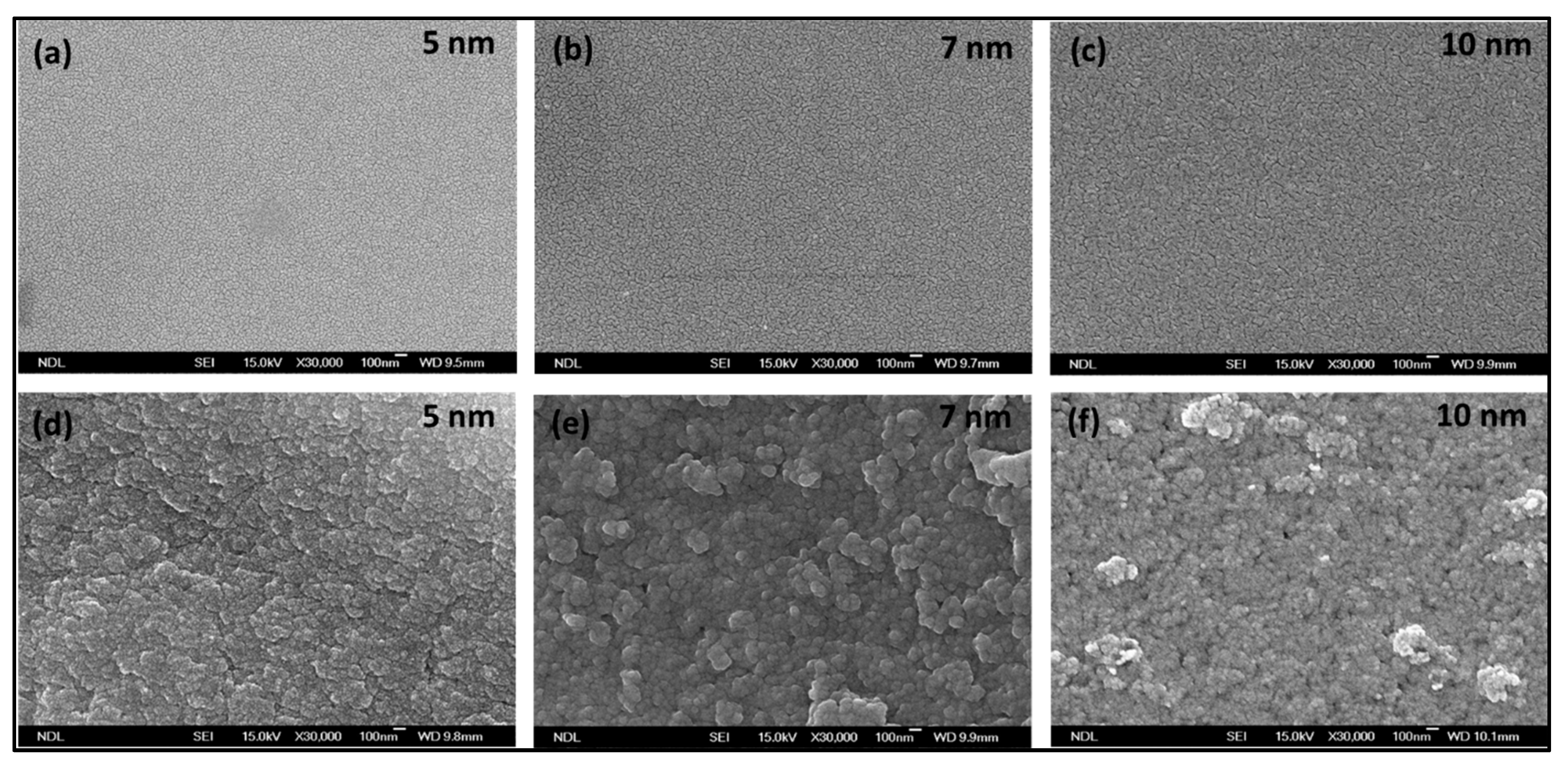
Scanning electron microscope (SEM) topography of the fabricated Si–Au and PSi–Au with different thicknesses is shown in
Figure 2a–c and
Figure 2d–f, respectively. SEM top view of Si after Au deposition was featured by the quality smooth surface and homogenous distribution of Au for all of the three Au–Si films of 5, 7, and 10 nm thickness, which in fact relies on the crystallographic orientation and smooth surface roughness of the starting Si substrate [
16]. On the other hand, the surface view of the PSi substrate coated with Au nanofilm of different densities shows irregular/tubular morphology; 7 nm Au–PSi shows the morphology of almost globular-shaped particles with agglomerated state. It is to be noted that the 10 nm Au–PSi, though having rough surfaces, showed no specific nanocrystallite shape, nor the compact arrangement. Due to the surface morphology of PSi, which depends on the crystallographic orientation of the crystal silicon wafers, as well as the nanopores and the surface roughness features of PSi which are defined by the etching conditions, a large number of nucleation sites are generated for the nucleation and growth of Au nanostructures than the smooth Si surface, hence influencing the morphology of the deposited Au thin films [
15,
26].
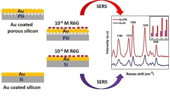
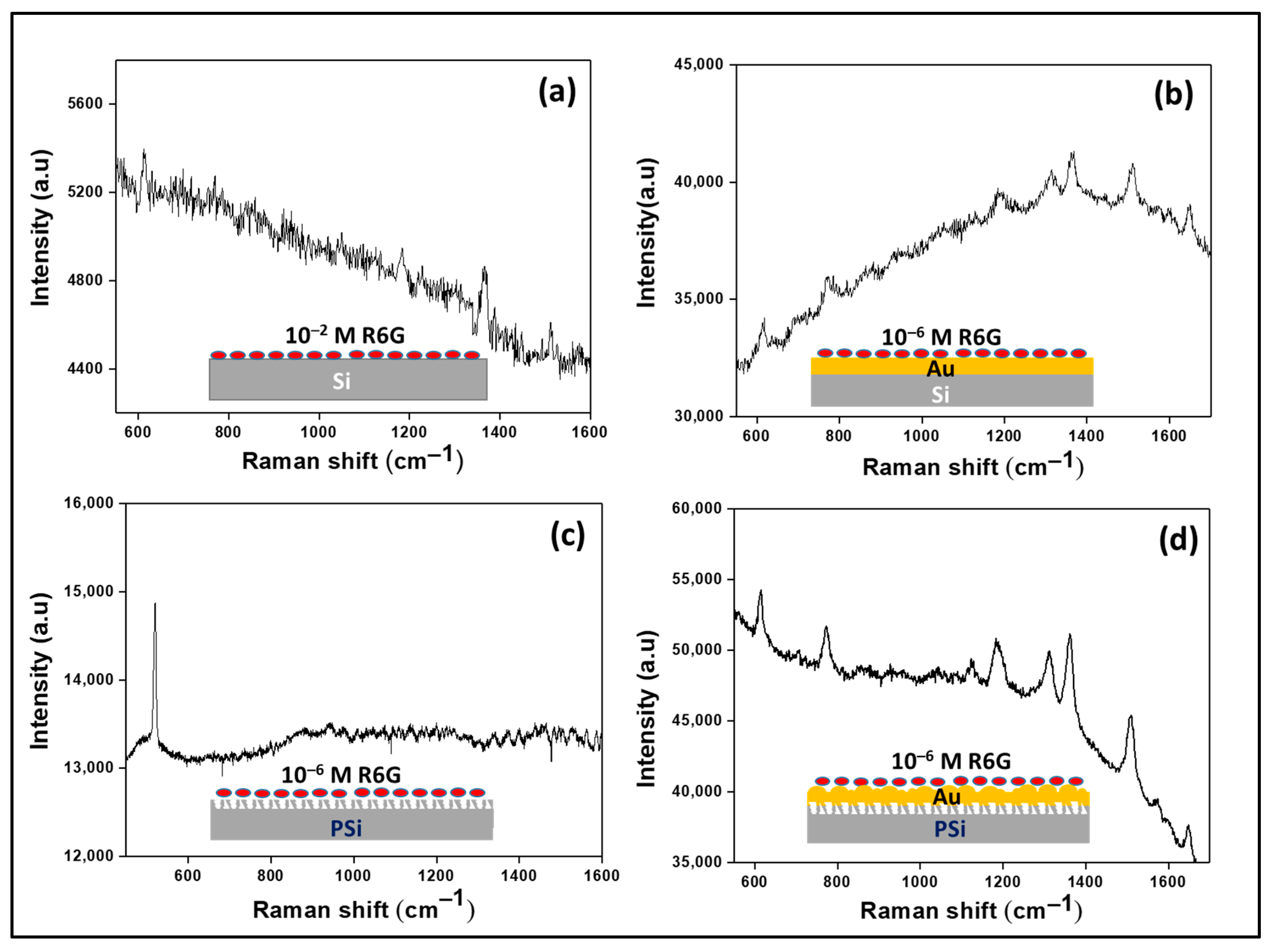
To verify the ability of PSi–Au as SERS substrate, a SERS study was conducted using bare PSi as a control substrate, while Si wafer with and without Au thin film as the reference platforms.
Figure 3 shows the schematic of each substrate for Raman measurement and the corresponding Raman spectra without normalization. Obviously, the PSi–Au exhibited the best performance as a SERS substrate.
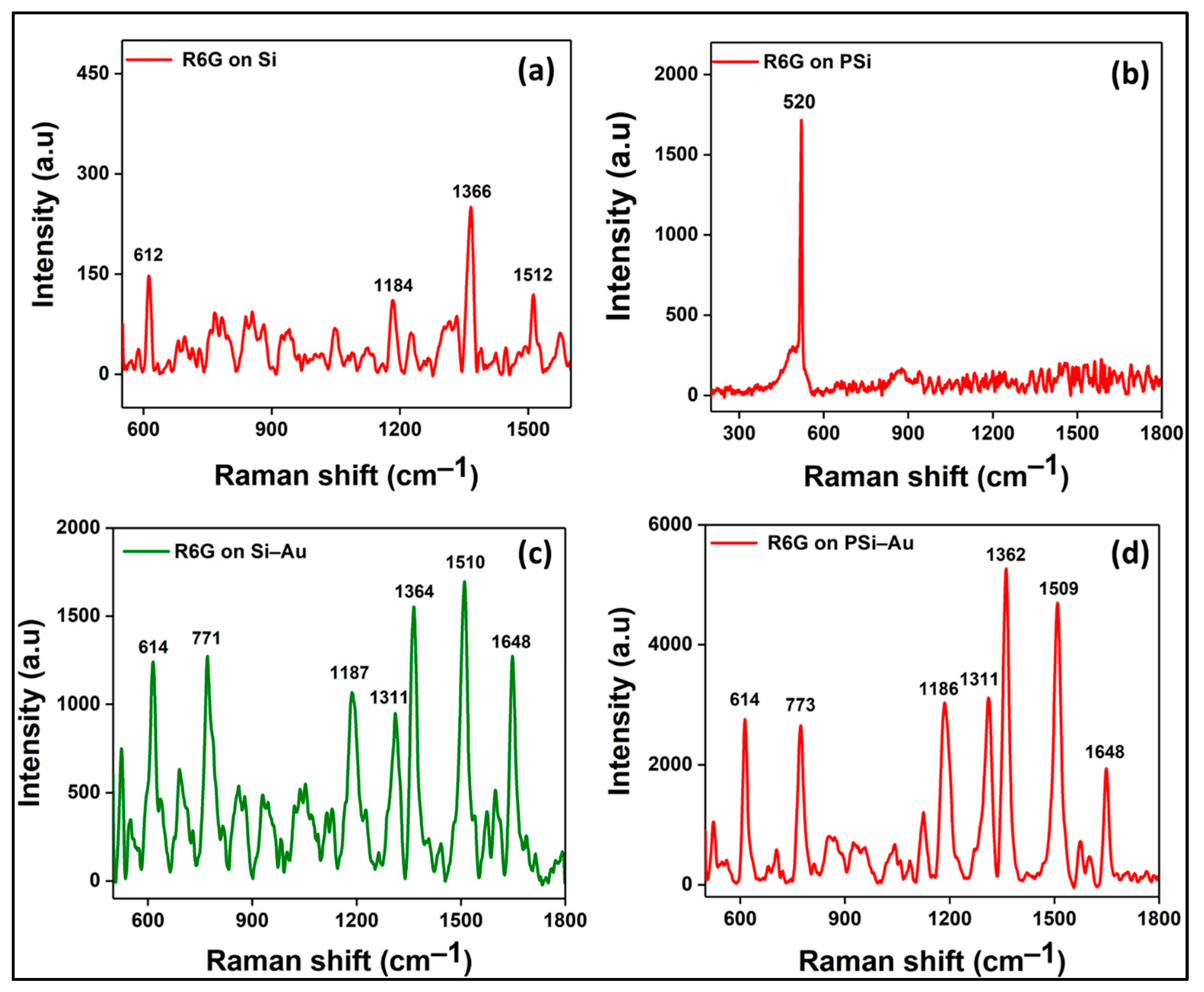
Figure 4 shows the normalized Raman spectra from different experimental conditions for better comparison of the Raman signal observed from different SERS substrates. In the study, bare Si wafer treated with a high concentration of R6G (10
−2 M) and the corresponding Raman spectra were characterized with major fingerprint peaks of R6G at 612, 1184, 1366, and 1512 cm
−1 (
Figure 4a). However, the bare PSi treated with a lower concentration of R6G dye (10
−6 M) did not produce any distinct and characterized peaks (
Figure 4b). On the other hand, coating of both Si and PSi templates with Au thin films, and subsequent treatment with the lowest concentration of R6G dye (10
−6 M), produced intense and more R6G fingerprint peaks (
Figure 4c,d). R6G assigned peaks for the Si–Au substrate were revealed at 614, 771, 1187, 1311, 1364, 1510, and 1648 cm
−1, while for PSi–Au substrate, the peaks were observed at 614, 773, 1186, 1311, 1362, 1509, and 1648 cm
−1.
Figure 4c,d exhibited a little peak shifting only in few instances. However, the vibrational spectra of R6G for both normal Raman and SERS study comply with previously reported studies [
15,
27]. The intensity of the well distinguished peaks generated on both SERS platforms demonstrated a remarkable enhancement, which is due to the electromagnetic enhancement and the chemical enhancement, due to the charge transfer mechanism between the adsorbed R6G and Au crystallites in the corresponding Au thin film substrate. The huge electromagnetic enhancement is due to the hot spots generated at the junctions between the platform components or among the Au crystallites assembled in the thin film [
5,
28].
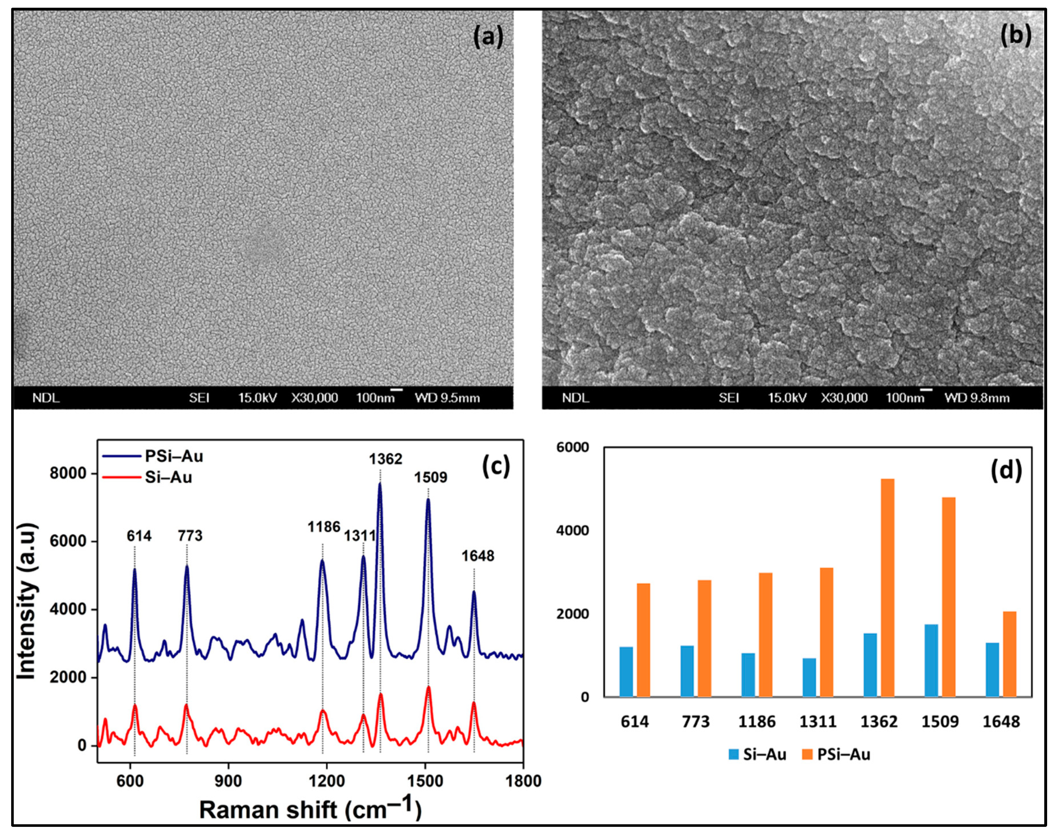
Moreover, SERS study of PSi–Au versus Si–Au was conducted to understand the impact of the porous structure of PSi on SERS effect. From the SEM topography, structural differences between the two platforms were also observed. Si–Au thin film was featured by homogenous distribution of the Au particles with smooth surfaces (
Figure 5a). On the contrary, PSi–Au thin film was characterized by the tubular particle structures in aggregated form with rough surfaces (
Figure 5b). However, both Si–Au and PSi–Au thin films produced identical, well distinguished, and intense SERS spectra with R6G fingerprints peaks (
Figure 5c). R6G adsorbed on PSi–Au thin film produced more intense peaks than Si–Au thin film (
Figure 5d). This greater intensity of PSi–Au thin film is due to the porous structure of the composite itself, surface roughness, size of the Au nanoparticle structure in thin film, and the agglomerated condition of the Au nanostructure on PSi (
Figure 5b), which facilitated the formation of higher number of electromagnetic hot spots at the inter-particle junctions [
5,
15]. Moreover, the enhancement factor (EF) value of the fabricated PSi–Au and Si–Au in comparison to the source Si wafer was determined by applying the equation
I
SERSSERSI
RamanC
Raman[
27]. Here, I
SERS is the SERS intensity of the R6G on the PSi–Au or Si–Au substrate, and C
SERS is the corresponding concentration of the R6G analyte (10
−6 M). On the other hand, I
Raman stands for the Raman intensity of the R6G analyte on Si wafer, and C
Raman is the corresponding R6G dye concentration of (10
−2 M). Hence, according to the experimental data (
Figure 5c,d), the EF of the PSi–Au and Si–Au substrates was calculated from the average SERS intensities of the major fingerprint peaks of R6G at 612, 1184, 1362, and 1510 cm
−1. The calculated average EF values are 2.7 × 10
5 for PSi–Au substrate and 9.7 × 10
4 for Si–Au substrate, and the increment of the EF value for the PSi–Au substrate in comparison to Si–Au is around 176%
Figure 5c,d.
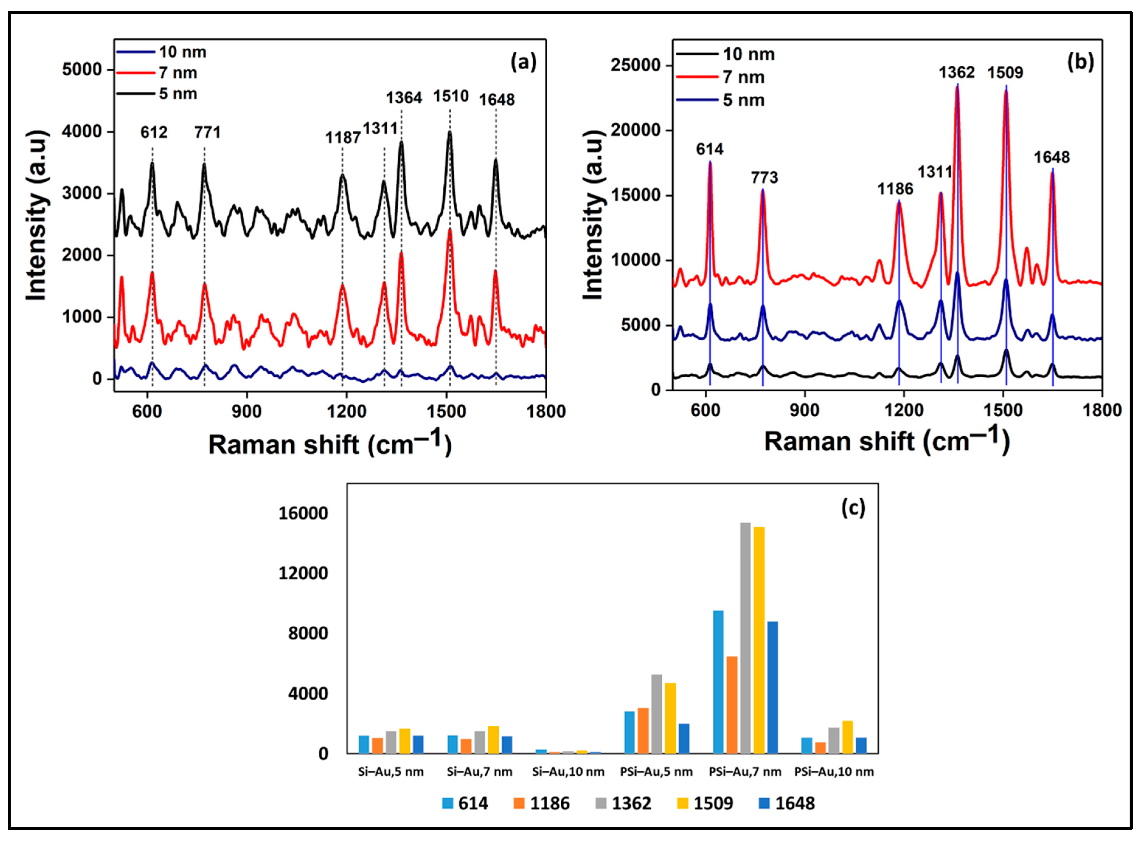
SERS spectra of R6G dye adsorbed on Si wafer coated with 5, 7, and 10 nm thin Au films are presented in
Figure 6a. Among the three layers, SERS spectra of 5 and 7 nm Au thin layer-coated Si wafer produced R6G fingerprint peaks which are more intense and well distinguished in comparison to 10 nm thin film. Among the three composites, Si–Au thin film of 7 nm proved the best substrate for SERS enhancement of R6G Raman tag (
Figure 6c). On the other hand, SERS spectra of PSi-coated Au thin films with the same thickness as of Si–Au also showed the same trend of SERS intensity (
Figure 6b). PSi–Au thin film of 7 nm thickness showed the highest SERS spectra, while 10 nm the least intense spectra, but still well distinguished. However, there is a clear distinguishing feature among the R6G SERS spectra between the two platforms, PSi–Au and Si–Au thin films. The greater SERS intensity of PSi–Au thin films is due to the increased surface roughness and in-homogeneity of Au nanocrystallite distribution on PSi surface, as well as the bigger particle size of nanocrystallites [
15]. Furthermore, the in-homogeneity of Au nanocrystals causes the generation of hot spots due to the coupling of the electromagnetic field of the adjacent particles and the consequent enhancement of localized surface plasmon resonance.
However, declining of the SERS intensity of R6G signatory peaks exhibited the same trend for both composites, a gradual increase from 5 to 7 nm with the best output, followed by sharp decline of the peak intensity for the 10 nm thickness. The lower SERS intensity at 5 nm Au film thickness could be explained by the presence of smaller Au size due to short e-beam deposition time, hence localization of R6G to these smaller Au nanocrystals had significant SERS effect [
16]. On the other hand, 7 nm Au film obtained after a few more seconds of progression of e-beam deposition generated Au nanocrystal of comparatively bigger size. Moreover, the inter-nanoparticle distance reached an optimized state to overlap the electromagnetic field to generate hot spots at the junctions of nanoparticles, hence generated hot spots mediated SERS signal amplification of the adsorbed R6G molecules. However, as deposition time was continued to achieve 10 nm thickness Au film, the corresponding SERS signal intensity of R6G molecules was observed to be significantly low. This might be due to the tightly packed Au nanocrystallites, where the interparticle distance was lapsed to form a continuous thick layer of Au film, acted like bulk Au material. As a result, there was no hot spot generation to amplify the SERS signal [
16,
29].
Similar results were also observed by another few experiments. For example, Kassu et al. conducted an experiment with nanoporous anodic aluminum oxide (AAO) substrates of a range of pore sizes (18, 35, 55, 80, 100, and 150 nm) coated with 30-, 40-, 50-, 60-, 70-, 80-, 90-, 100-, and 120-nm-thick Au films. Here, the thick films of 50 to 80 nm exhibited the best results, while both the initial (30 and 40 nm) and the end (90 to 120 nm) showed reduced intensity [
30]. Another study conducted by Dridi et al. fabricated Au–PSi substrate by e-beam deposition of Au on the rough Si backside at room temperature, and thickness of the Au film was regulated by varying the deposition time from 10 to 30 s. The corresponding SERS spectra of PSi–Au film for deposition time (t) below t = 15 s for both <100> and <110> orientation, showed a sharp decrease from higher to lower intensity. However, SERS intensity reached its maximum at t = 20 s for <100> orientation and at t = 20 and 25 s for the <110> orientation and at t = 25 and 30 s SERS intensities were at the lowest for <100> and <110> orientation, respectively. Therefore, our study proved that the thin films of Au on Si or PSi substrates are the active substrates for SERS enhancement. Among the two different platforms, PSi contributed more in SERS enhancement in comparison to Si wafer only. Though both types of SERS substrates were coated with the same three different layer Au thin films, however random surface roughness, densely packed and agglomerated nanoparticles of bigger size in PSi–Au thin films favor the generation of more hot spots in comparison to Si–Au thin films, hence leading to the significant enhancement of the SERS signals. Therefore, it could be concluded that SERS signal of the adsorbed R6G molecules depends on two main factors; firstly, the surface roughness features and crystallographic orientation of the silicon template, which ultimately defines the morphology, size, and arrangement of crystallites of the coated Au films, and secondly, the thickness of the Au layer.

 and
and 


