Article

Study on Femtosecond Laser Processing Characteristics of Nano-Crystalline CVD Diamond Coating

School of Mechanical and Electrical Engineering, Anhui Jianzhu University, Hefei 230601, China
*
Author to whom correspondence should be addressed.
Appl. Sci. 2019, 9(20), 4273; https://doi.org/10.3390/app9204273
Submission received: 5 September 2019 / Revised: 30 September 2019 / Accepted: 8 October 2019 / Published: 12 October 2019
(This article belongs to the Special Issue Ultrafast Optics: Trends and Prospects)

Abstract

:

Featured Application

This work should make an important contribution to the field of performance-enhancing of NCD-coated tools.

Abstract

Ultra-short pulse laser interaction with diamond materials has attracted extensive interest in micro- and nano-machining, especially for the fabrication of micro tools, because of the straightforward method and high precision. Thanks to the development of chemical vapor deposition (CVD) technology, high-quality CVD diamonds are employed in more varieties of tools as performance-enhancing coatings. The purpose of the experiments reported here was to explore the machinability of CVD diamond coating under the irradiation of femtosecond (fs) pulsed laser. The factor-control approach was adopted to investigate the influence of scanning speed, single pulse energy and repetition rate on the surface quality and carbon phase transition of CVD diamond coating. The material removal rate and surface roughness were evaluated. The interaction mechanism of scanning speed, single pulse energy, and repetition rate were discussed, and the fs laser ablation threshold of CVD diamond coating was calculated. It was demonstrated that two ablation mechanisms (weak and intensive) were in existence as evidenced by the distinct surface morphologies induced under different processing conditions. A strong dependence on the variation of scanning speed and pulse energy is identified in the examination of surface roughness and removal rate. Lorentzian–Gaussian deconvolution of Raman spectra illustrates that fs laser irradiation yields a strong modification effect on the coating and release the compressive stress in it. Furthermore, a newly defined parameter referring to the fs laser energies applied to unit volume was introduced to depict the degree of ablation and the Taguchi method was used to figure out the significance of different parameters. The ablation threshold of CVD diamond coating at the effective pulses of 90 is calculated to be 0.138 J/cm2.

1. Introduction

As a typical ultra-hard material (Vickers hardness ~100 GPa), diamond is an ideal candidate for ultra-hard tool fabrication for its outstanding properties such as super high hardness, extreme low expansion coefficient, and so on. In addition to being directly used as blank materials for micro tool fabrication, another widespread application of diamond is to deposit it on various tool surfaces to improve their working performance. Especially with the development of chemical vapor deposition (CVD) technology, that technology has become the preferred method to prepare high-quality diamond film with high efficiency and low cost. The usage of CVD diamond films as performance-enhancing coatings has already been extensively adopted in various complex shape tools [1], wire drawing dies [2,3], and other important components, and it exhibits outstanding performance and promising prospects for future development. However, the limitations of its traditional machining in efficiency, accuracy, and flexibility may pose an obstacle to the further application of diamond tools. The mentioned problems can be effectively solved by adopting femtosecond (fs) laser processing technology in the machining of diamond tools. At present, fs laser processing technology has been successfully applied across various industries for its material versatility [4,5,6,7,8] and found its place in ultra-precision machining owing to its ultra-short pulse width and high spatial resolution. In addition, the excellent geometric flexibility of laser machining makes it possible to fabricate complex micro or nano three-dimensional structures by fs laser processing. The past decade has seen a wide application of fs laser processing technology on the fabrication of various micro ultra-hard tools, such as the binder-less polycrystalline diamond micro-milling tool [1], the nano-twinned cubic boron nitride micro cutting tool [9], the positive rake angled single-crystal diamond (SCD) grinding tool [10], and so on. Besides bulk processing, surface modification of diamond is another hot research spot. A large number of researchers have studied the influence of fs laser parameters [11,12,13] and the pattern of surface textures [14,15,16,17,18,19] on tool processing performance. It has been proved that the fabrication of surface micro-textures is favorable to the tribological properties and lubrication behaviors of tools [20,21].
Since fs laser processing technology has great advantages in diamond-made tool bulk processing and surface modification, it is necessary to understand the mechanism and pattern of fs laser-diamond interaction, thus further expanding the application field of fs laser processing technology. Recently, there have been many reports on the exploration of fs laser-diamond interaction mechanisms. Liang et al. [22] have proposed a numerical model to predict the width of the ablated channel and calculate the fs laser ablation threshold of materials. The predicted results are close to the experimental results with a negligible error. Zavedeev et al. [11] obtained the single femtosecond pulse ablation threshold of diamond-like carbon (about 0.35 J/cm2) by observing the radius variation of irradiated spots. Chen et al. [12] calculated the single femtosecond pulse ablation threshold of the SCD to be 8.80 J/cm2 by the lnφ-D2 fitting method, and they also figured out the optimum fs laser processing parameters according to the experimental results. With respect to the polycrystalline diamond(PCD) material, many researchers have investigated the influence of ultrashort laser-induced ablation on its surface roughness [23,24] and dimension(depth and width) [24,25] in the nanosecond, picosecond, and femtosecond regimes. It can be concluded from those works that a shorter pulse duration, lower laser power (or single pulse energy), higher scanning speed and pitch can achieve a higher surface quality. However, too little work has been devoted to the interaction mechanism of working laser parameters or the effect of fs pulsed laser ablation on nanocrystalline diamonds (NCD). Films having grains in the nanometer range can be called NCD, which has both excellent properties of diamond material and nano-material. Compared with the traditional micron-scale PCD, there is a lot of graphite and amorphous carbon phase in the grain boundary of NCD, which thus exhibits a lower hardness and higher friction coefficient. In addition, as the grain size decreases to the nanometer scale, the intensity of diamond peaks of the Raman spectra reduces sharply, or may even be concealed by impurity-excited peaks, which makes the Raman spectrum of NCD distinct from that of PCD [26]. Herein, the study of fs pulsed laser processing of NCD should make an important contribution to the field of performance-enhancing of NCD-coated tools.
In this paper, three experimental schemes were designed to study the influence of the single pulse energy and the effective number of pulses on surface quality, carbon phase transition, and material removal rate of CVD diamond coating. Then, the interaction of scanning speed, pulse energy, and repetition rate was investigated by proposing a newly defined parameter EUV (energies applied to unit volume) and by conducting a Taguchi experiment. Finally, the saturated ablation threshold of CVD diamond coating was calculated based on the experimental results.

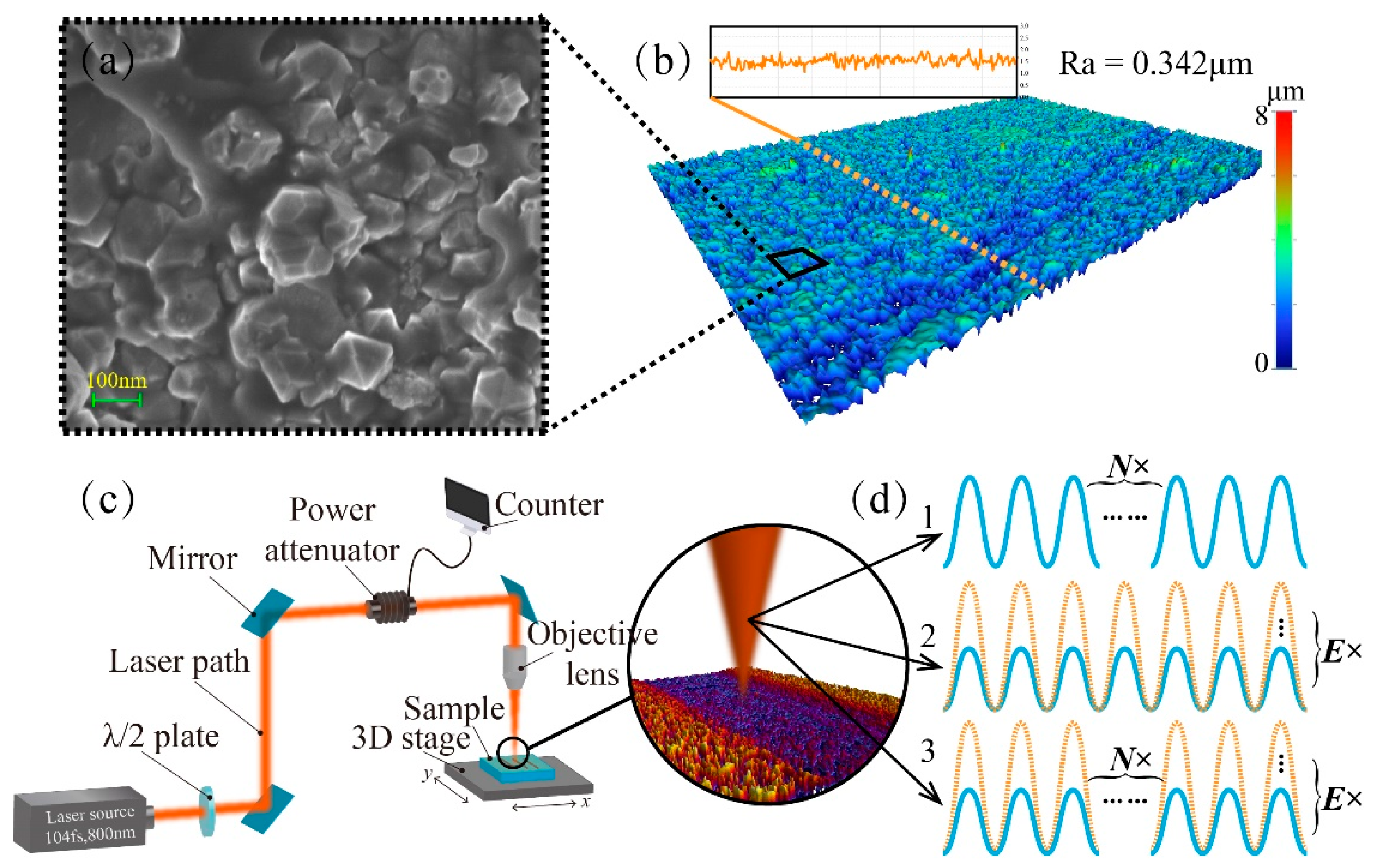
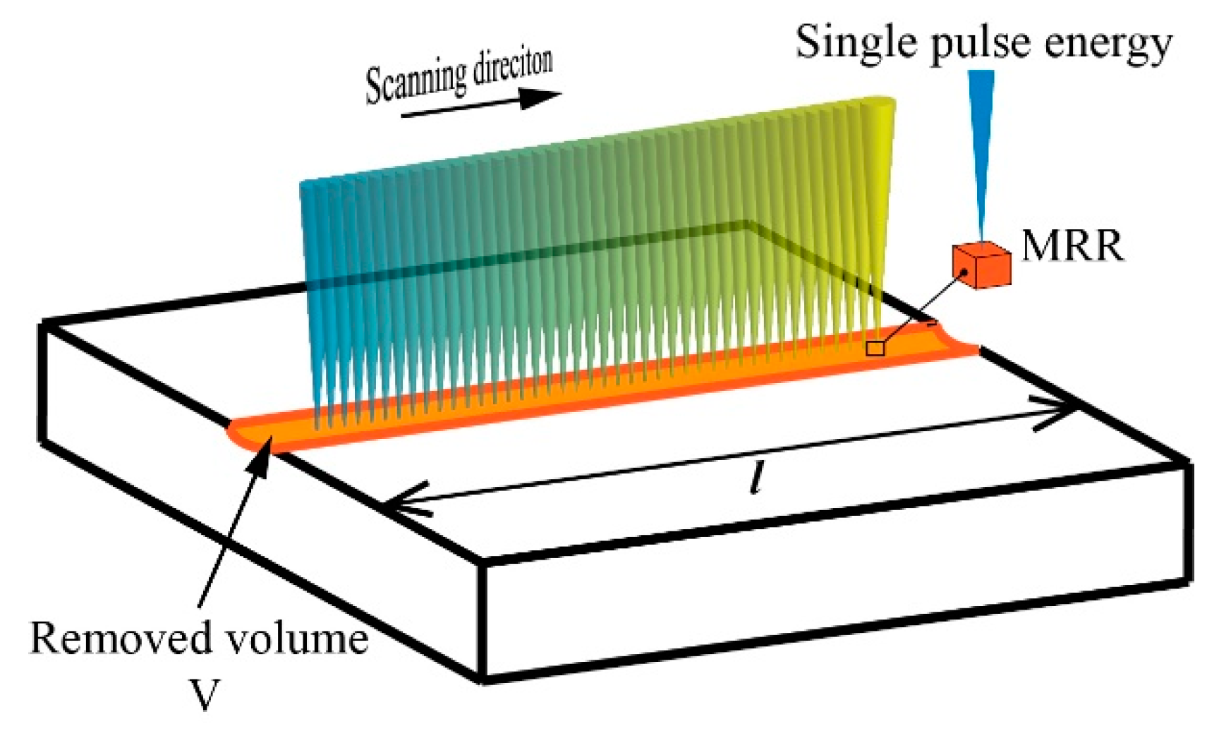
2. Experimental and Calculation Details

YG6 cemented carbides (ωWC = 94%, ωCo = 6%, density of 14.6–15.0 g.cm−2, thermal conductivity of 75.55 W·m−1·K−1, hardness(HRA) of 89.5, bending strength of 1.42 GPa) 10 mm × 10 mm × 3 mm in dimension were used as substrates and high-quality diamond films were deposited on the substrates through a bias-enhanced hot filament chemical vapor deposition system. The deposition condition of the diamond films is listed in Table 1. The surface morphologies of CVD diamond coating are depicted in Figure 1. It is visible from Figure 1a that the average grain size of a diamond crystal, of approximately 100 nm, is smaller than the size of normal diamond particles, suggesting that the obtained diamond grains in the coating are nanoscale. The average surface roughness of the original as-grown surface derived from topography is measured at 0.342 μm, and the cross profile shows a homogeneous morphology of the coating surface (see Figure 1b).
The applied fs laser pulses of 100 fs duration generated by a Ti: Sapphire laser system (America, Coherent), operating at the wavelength of 800 nm, an 8 × objective, which can provide a beam waist diameter of 30 μm measured at the 1/e intensity, was used to perform the ablation experiments. The schematic drawing of the laser processing setup is depicted in Figure 1c. The fs laser beam propagates from the laser source to the objective lens by mirrors and is vertically irradiated on the diamond coating surface in the ambient air. The ablation results of diamond coating essentially rely on two parameters of the femtosecond laser, i.e., single-pulse energy, E, which directly determines the value of laser fluence, and the effective number of pulses, N, which contributes to the incubation effect. In this work, we investigated the influence of three fs laser conditions on the ablation results. The three conditions are as follows: Changing Ep and N separately and changing both the two parameters at the same time, as illustrated in Figure 1d.
In the case of continuous scanning, the laser focus point will overlap with each other, so it is more appropriate to investigate the influence of the number of accumulated pulses per unit area, i.e., the effective number of pulses, on the ablation results than to simply consider the influence of repetition rates. The effective number of pulses, N, can be calculated by Equation (1):
N = k 2 ω 0 f v ,
where k is the number of scanning times (all experiments in this work are single scanning, thus k = 1), ω0 is the beam waist, f is the repetition rate, v is the scanning speed. Therefore, the effective number of pulses can be adjusted by controlling the repetition rate or scanning speed. The scanning speed and direction can be controlled by the 3-axis translation stage with a position accuracy of 0.1 μm. The single pulse energy is regulated by the attenuator. The processing parameters used for ablation are given in Table 2. The surface morphologies of the diamond coating were observed by field emission scanning electron microscope (Zeiss, GeminiSEM500). Confocal Raman spectrometer (Renishaw, inVia Reflex) was employed to evaluate the carbon phase of the coating. A white-light (WL) interferometer (Bruker, ContourGT-K) was used to measure the average roughness of the laser-irradiated regions and the material removal rate.

3. Results and Discussion

3.1. Influence of Effective Number of Pulses on CVD Diamond Coating Ablation

It can be found from Equation (1) that the effective number of pulses correlates to both repetition rate and scanning speeds. In this part, the effective number was adjusted separately by changing scanning speeds.
SEM photographs of the diamond coating surface irradiated at different scanning speeds, with a pulse energy of 100 μJ, and repetition rate of 1 kHz are demonstrated in Figure 2. It can be seen from Figure 2 that the sharp pointedness of diamond grains was polished by laser ablation and the initial homogeneous structure was taken over by deep subwavelength ripples. The periodical ripples or laser-induced periodic surface structure (LIPSS) derive from the interference of the incident laser with quasi-monochromatic plasmons or among themselves. In this regime, the produced periodicity of LIPSS, approximately λ/4, is much smaller than λ [27], and can be calculated as ʌ = λ/2n = 167 nm for normal incidence, where λ = 800 nm is the wavelength of the fs laser applied in this work and n = 2.40 is the real part of the complex refractive index of diamond [28]. The orientation of the LIPSS is perpendicular to the laser polarization direction. When irradiated at high scanning speed, the laser-induced surface modification is less in extent for the reason of the small effective number of pulses, N. Although there is LIPSS in the irradiated region, it is not obvious because the gaps between the LIPSS have been filled by re-solidified materials. As the scanning speed decreases, which means a bigger N, excessive energy accumulates in unit area, leading to a strong incubation effect and inducing clear division among the periodical structures. Moreover, the width of ripples becomes narrower and longer, which is in line with the previous results found by A.F. Sartori et al. [29]. It has also been observed that a large number of melt slags showed up in the irradiated region.
The WL interferometer reconstructed topographies are displayed in Figure 3, with the upper profiles (blue) derived from the cross-section along the yellow horizontal line. The red profiles on the right are the cross-section obtained along the black vertical line. It can be found that there is little difference between the height of the irradiated region and that of the laser unaffected region when scanning at speed of 2 mm/s. With the decrease of the scanning speeds, the depth of the ablated grooves, which figures out the degree of ablation, increases gradually though the single pulse energy does not change. The tendency of the ablation depth indicates that the effective number of pulses (or the degree of incubation effect) plays a major role in the machining of the diamond coating. The surface roughness Ra and material removal rate (MRR) at the employed laser conditions are both based on the WL interferometer topography measurement. The obtained Ra and MRR vs. different scanning speeds are depicted in Figure 3f. As expected, the greater the scanning speed, the better the surface roughness. As the scanning speed rises from 1.2 mm/s to 2.0 mm/s, Ra decreases from 0.356 μm to 0.314 μm, indicating that the reduction of the effective number of pulses is beneficial for the polishing of the diamond coating surface. However, unlike the tendency of Ra variation, the MRR declines with the decrease of scanning speed, which obviously results from the fixed focal distance from the focus point to the diamond coating surface. That is to say, with the increase of the ablation depth, a defocus of the irradiation region occurs and finally renders the MRR descending.
In order to investigate the influence of fs pulsed laser ablation on the carbon phase transformation of the diamond coatings, a Lorentzian–Gaussian fit is applied to make deconvolution of the obtained Raman spectra of the samples. The original Raman spectra and the integrated deconvolution peaks are all shown in Figure 4, where Raman fit stands for the original data after the Lorentzian–Gaussian fit, TP is the fitted peak of trans-polyacetylene, AS is amorphous sp3 carbon, DIA is the diamond phase, D stands for D-band, and G stands for G-band.
During the CVD process, amorphous carbon and diamond particles are always co-deposited on the substrate surface, and the grain size of the deposited diamond coating is so small (see Figure 1b) that a large amount of graphite and amorphous carbon phase adhere to diamond grain boundaries. That non-diamond phase makes the Raman spectrum of nano CVD diamond coating always present a typical characteristic of a sharp diamond peak accompanied by wide D peaks. Meanwhile, compared with the microcrystalline diamond, the Raman spectra of the as-grown nano CVD diamond, also has a large G-band range of 1500 cm−1 to 1600 cm−1, as can be seen from Figure 4a. With the decrease of the scanning speed, the intensity of diamond peaks reduces gradually due to the laser-induced graphitization. The diamond peak disappears completely when the scanning speed decreases to 1.2 mm/s, and the Raman spectrum transforms to a typical graphite Raman line, suggesting the graphitization can be enhanced with the rising effective number of pulses. Moreover, the fitted diamond peaks have a shift toward lower wavenumbers (from the original 1335.24 cm−1 to 1332.52 cm−1 at 1.4 mm/s). This shift pattern indicates that the compressive stress in diamond coating introduced during deposition can be released by fs laser irradiation.

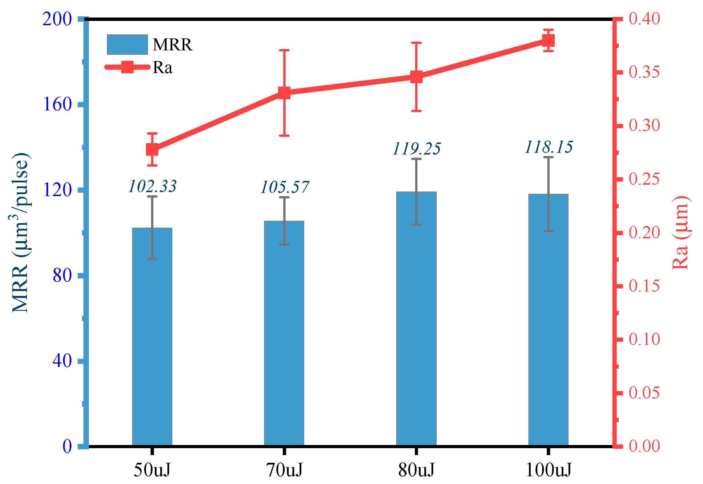
3.2. Influence of Pulse Energy on CVD Diamond Coating Ablation

SEM photographs of the diamond coating surface irradiated under different pulse energies at the scanning speed of 1 mm/s and repetition rate of 1 kHz are displayed in Figure 5. It can be found that the variation of pulse energies has a considerable influence on the morphology of the diamond coatings. When the pulse energy is low, the accumulated energy in the irradiated region is not enough to evaporate the materials but only to melt them. With the shifting of the laser spot, the melting materials re-solidified on the surface of the coating and compacted the arrangement of the laser-induced periodic structures owing to the abrupt temperature dropping, and the irradiated region showed a homogeneous morphology (see Figure 5a). When pulse energy rose to 80 μJ or higher, the morphology of the coating changed dramatically, displaying a loose periodic structure with a large number of melting slags adhering to them. In this stage, the ablation of the diamond coating combined with melting and vaporization. The melted materials could not re-solidify on the coating surface. Instead, they are vaporized by the intensive fs pulses.
The three-dimensional topographies of the diamond coatings produced under the given conditions are presented in Figure 6. It can be observed from the y profile of the coating surface that the depth of the irradiated region increased as the pulse energy rise from 50 μJ to 100 μJ. The surface roughness Ra and MRR are plotted against pulse energies in Figure 7. The tendency of the surface roughness is consistent with the variation of the x profile obtained along the irradiated grooves (see Figure 6). A strong dependency of Ra on MRR was observed under the given condition that the higher the MRR, the greater the Ra. The dependency of Ra on MRR observed in this part is in good agreement with the conclusion proposed by Sedao et al. [30]. It is easy to understand that when adopting high-energy to irradiate the target, the interaction between laser and target becomes more intensive, thus causing the surface smoothness to worsen.
The integrated deconvolution fitted Raman spectra of the diamond coating surfaces irradiated under different laser pulse energies are shown in Figure 8. As expected, increasing pulse energies is severely detrimental to the content of diamond. With the rise of the pulse energies, the diamond peak disappears finally. Again, consistent with the results discussed in Section 3.1, the compressive stress in the diamond coatings can be released by ablation enhancement. The Raman spectrum at 80 μJ shows a similar characteristic to the Raman spectrum at 1.2 mm/s in Figure 4f, suggesting the degree of ablation under the two processing conditions is close to each other, while the surface roughness under the two conditions also proves this point. Moreover, the relative intensity of D peaks increases significantly as pulse energy rises, which indicates a growth of sp2 hybridized carbon phases and serious dislocations in the diamond lattice.

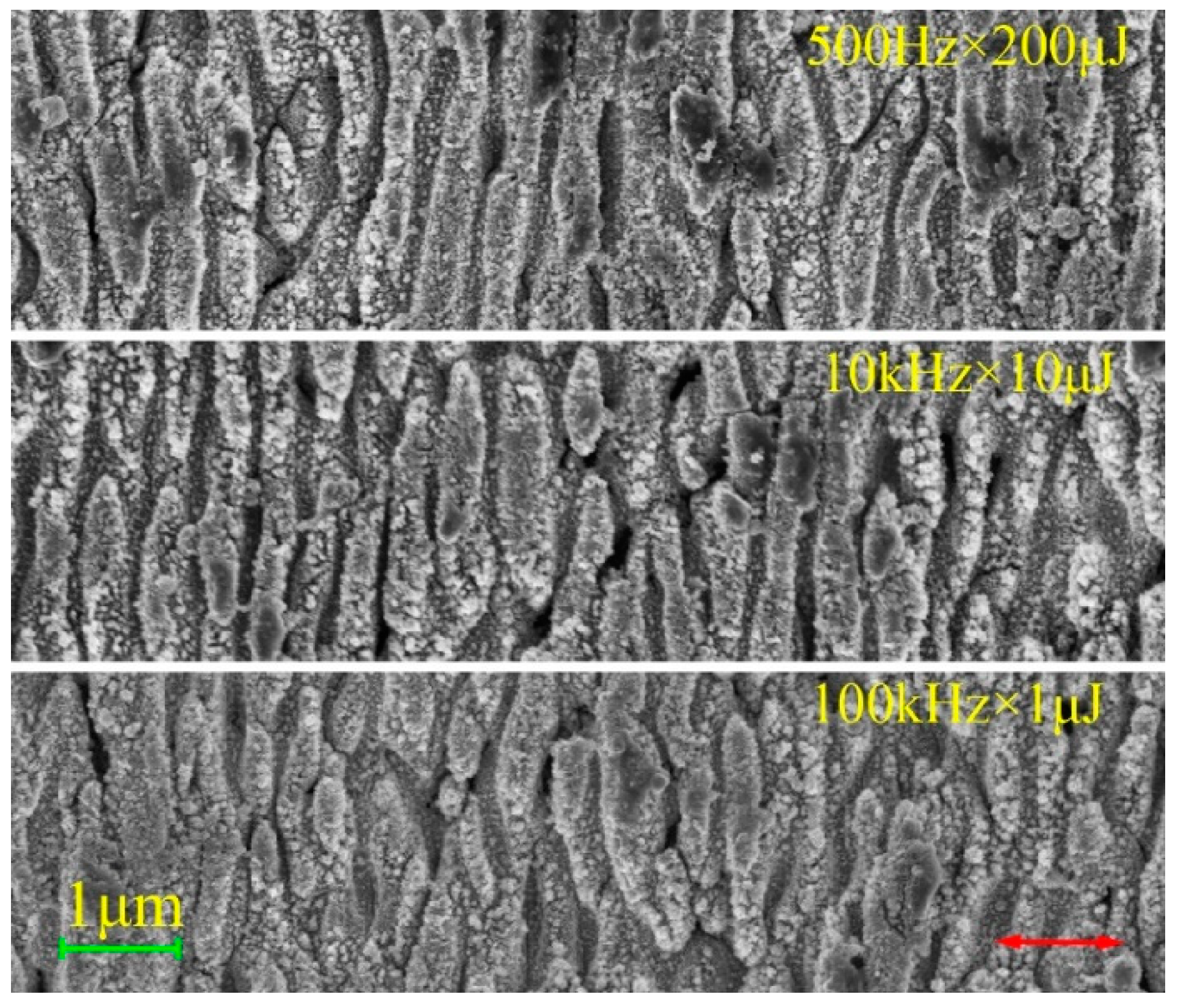
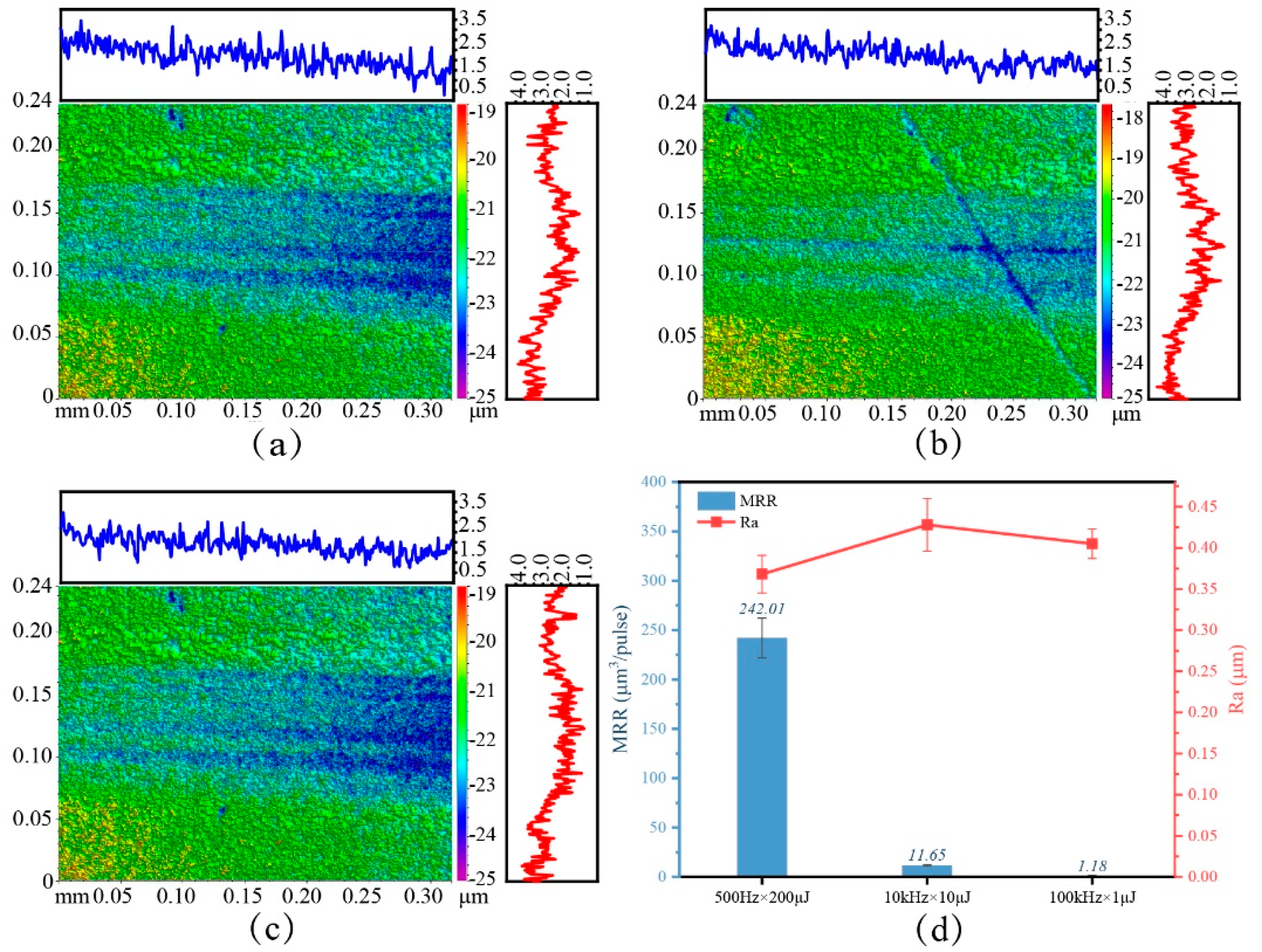
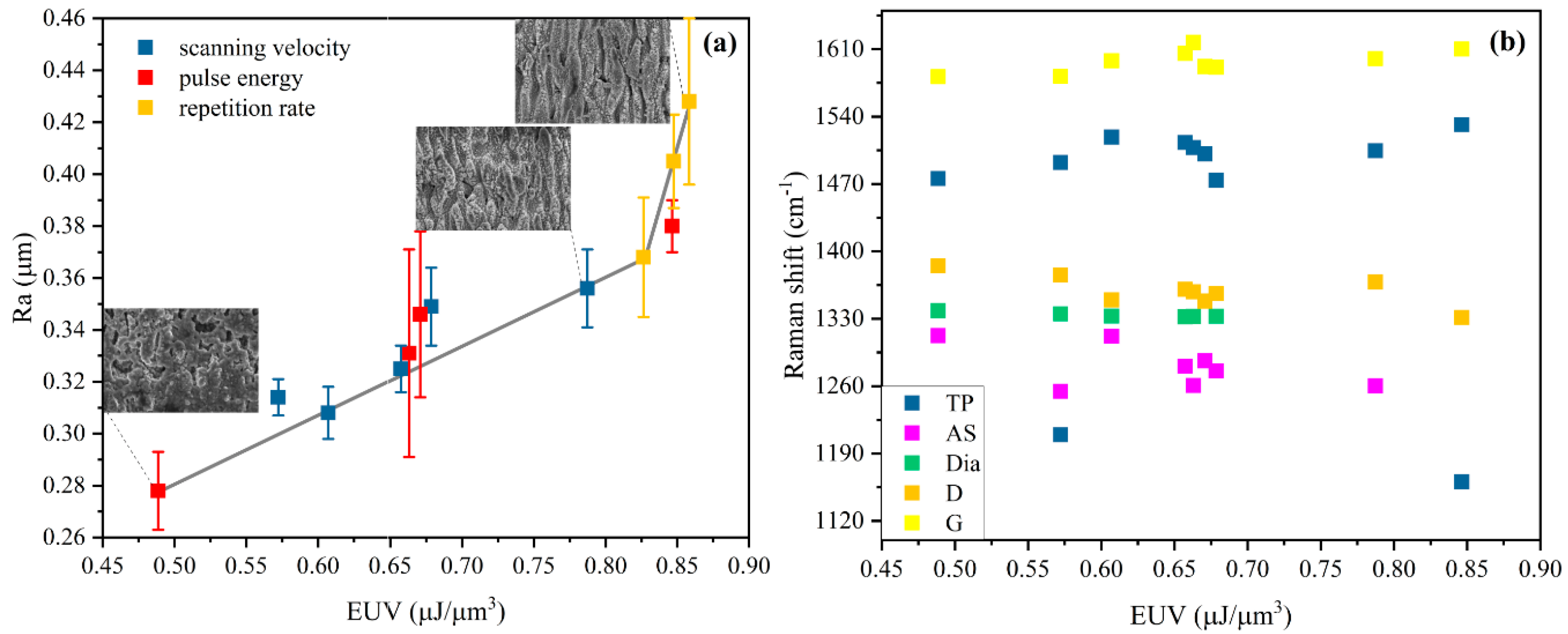
3.3. Influence of the Interaction of Pulse Energy and Repetition Rate on CVD Diamond Coating Ablation

In order to investigate the influence of the combination of single pulse energy and effective number of pulses on the ablation results of CVD diamond coatings, three conditions, namely, 500 Hz × 200 μJ, 10 kHz × 10 μJ, and 100 kHz × 1 μJ, are adopted by adjusting the single pulse energy and the laser repetition rate simultaneously. The scanning speed is 1 mm/s. Since average laser power, P, can be calculated by the following equation: P = Ef, it is easy to know that the average power of the three conditions is maintained at 100 mW. For the sake of clarity and comparability, the SEM photographs produced under the three conditions are combined into one picture (as seen in Figure 9). It is clear that morphologies produced under the three conditions exhibit uniform micro-structures, their LIPSS characteristics especially are almost identical.
Furthermore, as displayed in Figure 10a–c, either the white-light interferometer obtained topographies or the measured x or y profiles resemble one another to a large extent. It is interesting to find that the morphology and topography present in Figure 9 have many features similar to those in Figure 5d and Figure 6d, where the calculated average power is also 100 mW. Hence, we can reach a conclusion that regardless of how the single pulse energy or repetition rate changes (either separately or together), the final ablation results rely on the average power derived from these two parameters. This conclusion can also be evidenced by the Ra curve plotted in Figure 10d, where the roughness of the irradiated regions fluctuated around 0.4 μm. On the contrary, the MRR decreased sharply under the given conditions, and the MRR at 500 Hz × 200 μJ was almost 200 times higher than that of 100 kHz × 1 μJ.

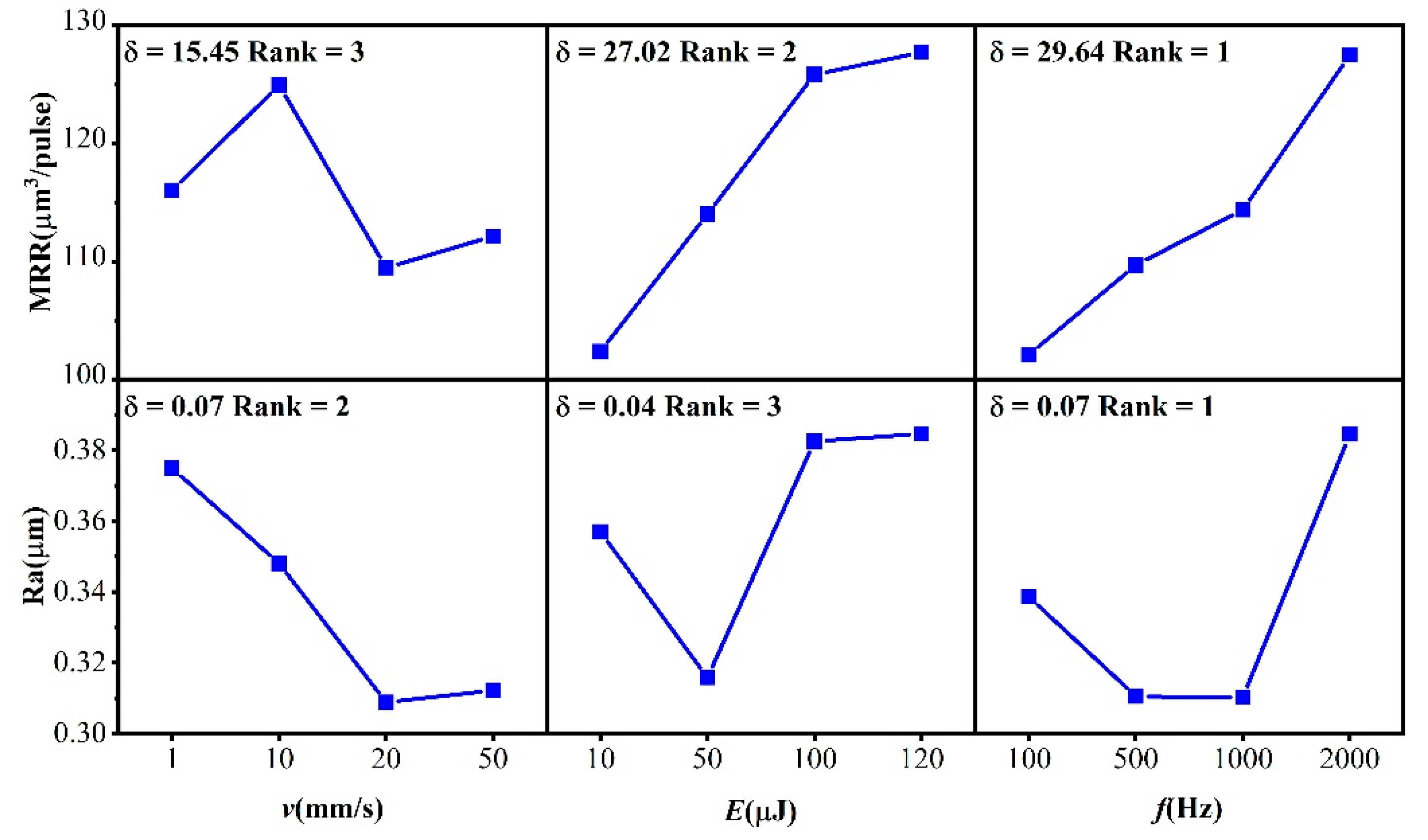
4. Interaction Analysis of Scanning Speed, Pulse Energy, and Repetition Rate

So far, we have discussed the influence of three factors, namely, scanning speed, v, pulse energy, E and repetition rate, f, on the fs laser ablation results of CVD diamond coating. Among them, the effect of v is equivalent to that of f, for they determine the effective number of pulses together. In the experiment of scanning speed change, the enhancement of ablation on diamond coating is caused by the strengthening of the incubation effect. In the single pulse energy change experiment, the promotion of ablation arises from the increase of laser fluence. Finally, under the co-affection of pulse energy and repetition rate, the ablation of diamond coating turns into a dynamic equilibrium between cumulative effect and influence of laser fluence, and the ablation degree can be figured out by examining the value of average laser power. The outcome of actual laser processing is the synergy of the interaction of v, p, and f. In the report of ns laser-induced reduction of graphene oxide, S.A. Evlashin et al. used energy fluences, which represent laser energies applied to unit area, to describe ns laser irradiation effects [31]. Inspired by this, we introduce a parameter embracing all three factors to depict the degree of fs laser ablation. The new parameter represents the fs laser energies applied to unit volume (EUV). Its value is equal to the ratio of single pulse energy to MRR, and can be further calculated by the following equation:
EUV = E f l V v ,
where l is the length of the irradiated region and V is material volume removed by fs laser irradiation. A schematic diagram of fs laser ablation is drawn in Figure 11. Three factors, E, v, and f, are taken into account in one parameter. Thus, we can simply focus on the EUV to evaluate the influence of fs laser irradiation. The adopted experimental conditions and corresponding EUV are listed in Table 3. The surface roughness Ra and Raman peak positions are re-plotted against EUV in Figure 12.
Impressively, as can be seen from Figure 12a, no matter how fs laser processing parameters change, the roughness of the material always increases with the increase of EUV. It is obvious that the morphologies of the irradiated regions experienced three stages as the EUV increasing. First, when the EUV is small, the surface of the diamond coating is covered by a layer of re-solidified materials. The edges and corners of the diamond grain of the initial coating surface are polished, and the LIPSS is not obvious because of the re-solidified materials coverage. Second, with the increase of EUV from the initial 0.49 μJ/μm3 to 0.79 μJ/μm3, the amount of re-solidified materials decreases, instead, there is a large number of white melted slags embed in LIPSS. During this progress, the slope of the fitted EUV-Ra curve is small, indicating a small increasing rate of the surface roughness. After that, the surface morphology of diamond coating begins to change abruptly and presents a typical clear LIPSS. At the same time, the surface roughness Ra increases sharply. These changes suggest that there are two stages of weak ablation and strong ablation in fs laser processing of diamond coatings, the boundary point appears at 0.83 μJ/μm3. In the weak ablation stage, the femtosecond laser energy applied on the target is small, which has far less effect on the surface modification than on the polishing and melting of the diamond coating, so the evolution of the morphologies of the irradiated region is moderate and diamond peaks can always be detected in Raman spectra (Figure 12b). In the stage of intense ablation, the mechanism of fs laser ablation of the diamond coatings is mainly vaporization and phase explosion. Typical LIPSS accompanied by severe graphitization (the diamond peak disappears after 0.78 μJ/μm3) appears in the laser-irradiated regions due to the extensive laser modification and surface roughness Ra increases rapidly with the rise of energy. Moreover, most of the laser energies are absorbed by graphite in the form of heat loss owing to the extremely high absorption coefficient of graphite, thus the ablation of the diamond coating is saturated in this stage.
Although EUV can reflect the ablation degree by considering the interaction of scanning speed, pulse energy, and repetition rate as a whole, it is interesting to further detail the significance of each parameter during the interaction progress. A Taguchi array of L16 (with three factors at four-level, outlined in Table 4) was produced and analyzed using Minitab 19 (Minitab, LLC., State college, Pennsylvania, USA) so that as much useful information as possible can be extracted from a predetermined and limited number of experiments. As can be seen from the response results for the signal-to-noise ratio of Ra and MRR highlighted in Figure 13, repetition rate showed the largest delta for both Ra and MRR, suggesting it has the most significant effect on the two features over the range studied. The scanning speed was found to be the second-ranked factor affecting the surface roughness, but to be the lowest-ranked factor in the MRR response, which means that the scanning speed plays a different role in achieving accuracy and efficiency. As can be seen from Figure 13, we can realize an optimal polishing processing by adopting v3 E2 f3 (scanning speed 20 mm/s, pulse energy 50 μJ, repetition rate 1 kHz). However, the most efficient parameter set turns out to be v2 E4 f4 (scanning speed 10 mm/s, pulse energy 120 μJ and repetition rate 2 kHz).

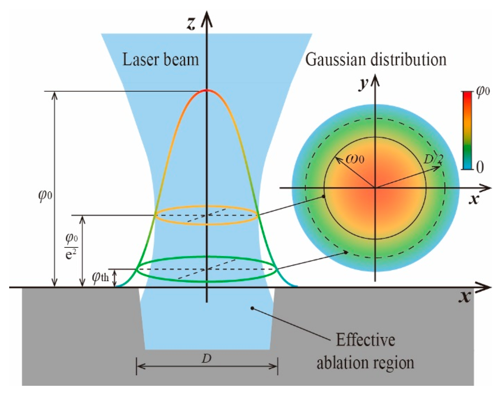
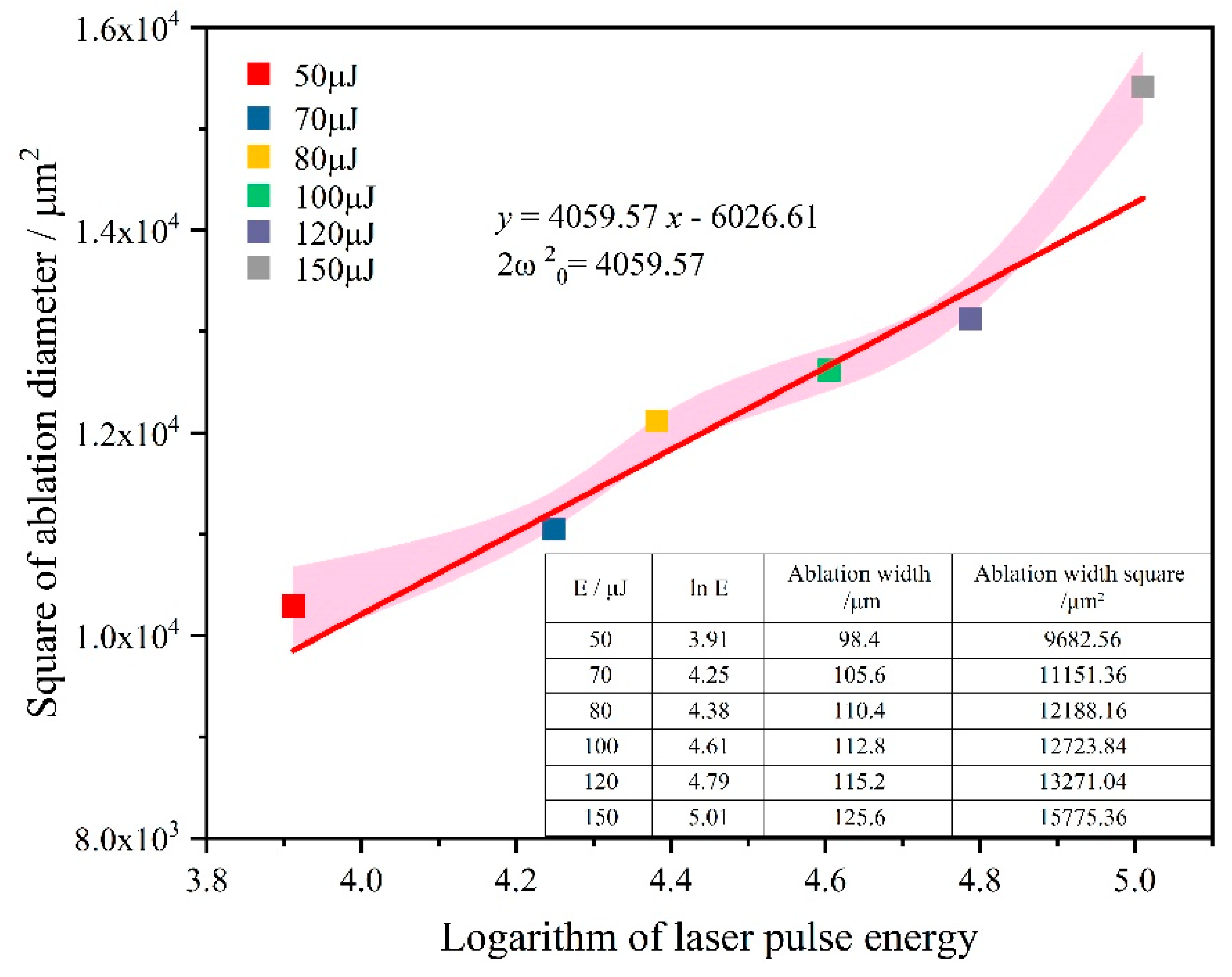
5. Femtosecond Laser Ablation Threshold of CVD Diamond Coatings

The laser ablation threshold of materials is the minimum laser energy density required to induce irreversible surface damage during laser-target interaction. Obtaining the ablation threshold of a specific material is of great significance to the study of its machinability. Since the single pulse energy of an fs laser obeys the Gauss distribution (see Figure 14), the laser threshold of material φth is equivalent to laser fluence at the border of the effective ablation region, which can be presented by Equation (3), as follows:
φ t h = φ 0 e D 2 / 2 ω 0 2 ,
where φ0 is the central energy density of fs laser and D is the diameter of the effective ablation region.
Thus,
D 2 = 2 ω 0 2 ( ln φ 0 ln φ t h ) .
Given the threshold fluence φth holds constant under a specific effective number of pulses, it can be found that the function represents a curve of the first degree with respect to independent variable lnφ0 and dependent variable D2 with a slope of 2ω02 and an x-intercept of φth. Since the relationship between laser fluence φ and single pulse energy E follows
φ = 2 E π ω 0 2 ,
Equation (4) can be expressed accordingly as the following equation:
D 2 = 2 ω 0 2 ( ln E ln E t h ) ,
where Eth is the threshold of single pulse energy under given conditions. In the case of continuous linear ablation of the diamond coating by an fs laser, multiple pulses arrive at the same spot. Thanks to the extreme narrow pulse width of the fs laser, which is much shorter than the thermal relaxation time, multiphoton absorption occurs and makes incubation effect severe. Some studies have suggested that the occurrence of the incubation effect enables the ablation threshold to be decreased, which is inversely proportional to the effective number of pulses [32]. It can be discovered from Figure 12a that when EUV equals 0.7873 (v = 1.2 mm/s), the ablation mechanism begins to transform from weak ablation to intense ablation, and when EUV reaches 0.8464 (v = 1 mm/s), the ablation of diamond coating is saturated. At this time, owing to the extremely high absorption coefficient of graphite, the material removal is hard to increase. Therefore, according to Equation (6), the saturated ablation threshold of CVD diamond coating can be calculated by obtaining the lnE-D2 curve at the scanning speed of 1 mm/s.
The beam waist ω0 and the threshold of pulse energy Eth can be obtained from lnE-D2 fitting (see Figure 15), and the laser ablation threshold of material φth can finally be calculated by Equation (5).
The obtained beam waist ω0 equals 45.05 μm and the threshold of pulse energy can be found at 4.41 μJ. Thus, the fs laser ablation threshold of NCD diamond coating is 0.138 J/cm2 under the effective pulses of 90, calculated by Equation (1). The calculated threshold is much smaller than that of SCD (8.80 J/cm2) [12] or PCD (1–1.6 J/cm2) [33].

6. Conclusions

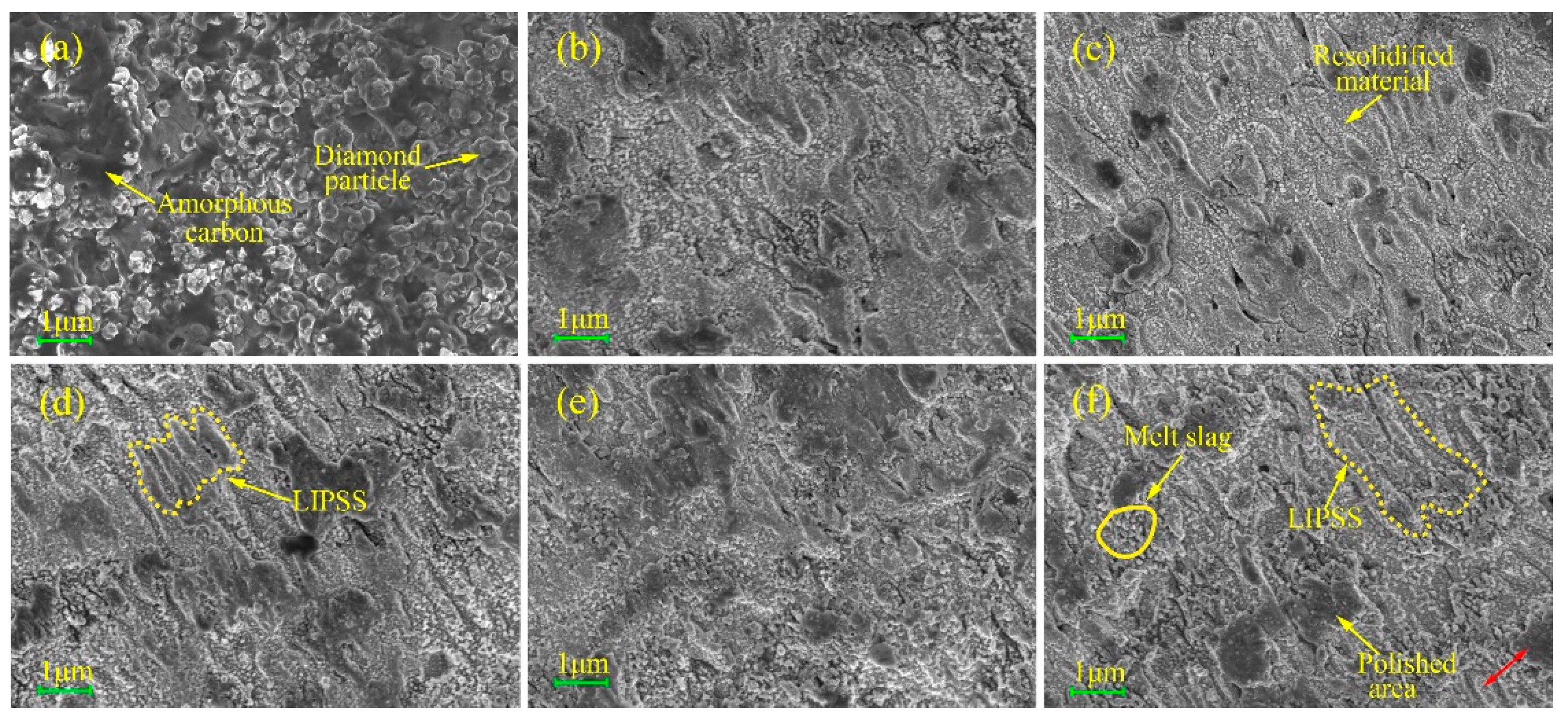
  • The analysis of morphologies revealed that under high scanning speed or low single pulse energy conditions, the surface of diamond coating experiences material melting and re-solidification progress. While with the decrease of scanning speed or rise of pulse energy (both result in a harsh condition), the ablation of diamond coating turns into a tri-stage mechanism of melting-graphitization-evaporation.
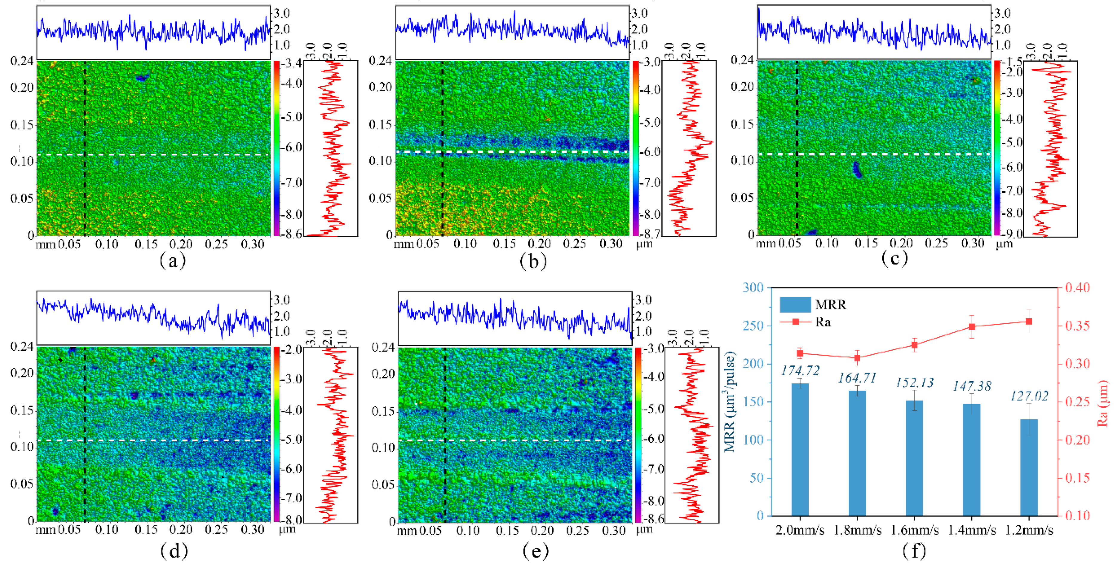
  • With respect to surface roughness and MRR evaluation, both surface roughness Ra and MRR show a strong dependence on the variation of scanning speed and pulse energy, yet they show the same tendency with scanning speeds compared to different ones when changing with single pulse energies. In addition, in the investigation of the co-effect of pulse energy and repetition rate, we found that the ablation results produced under different pulse energies or repetition rates can be figured out directly by examining the value of average laser power.
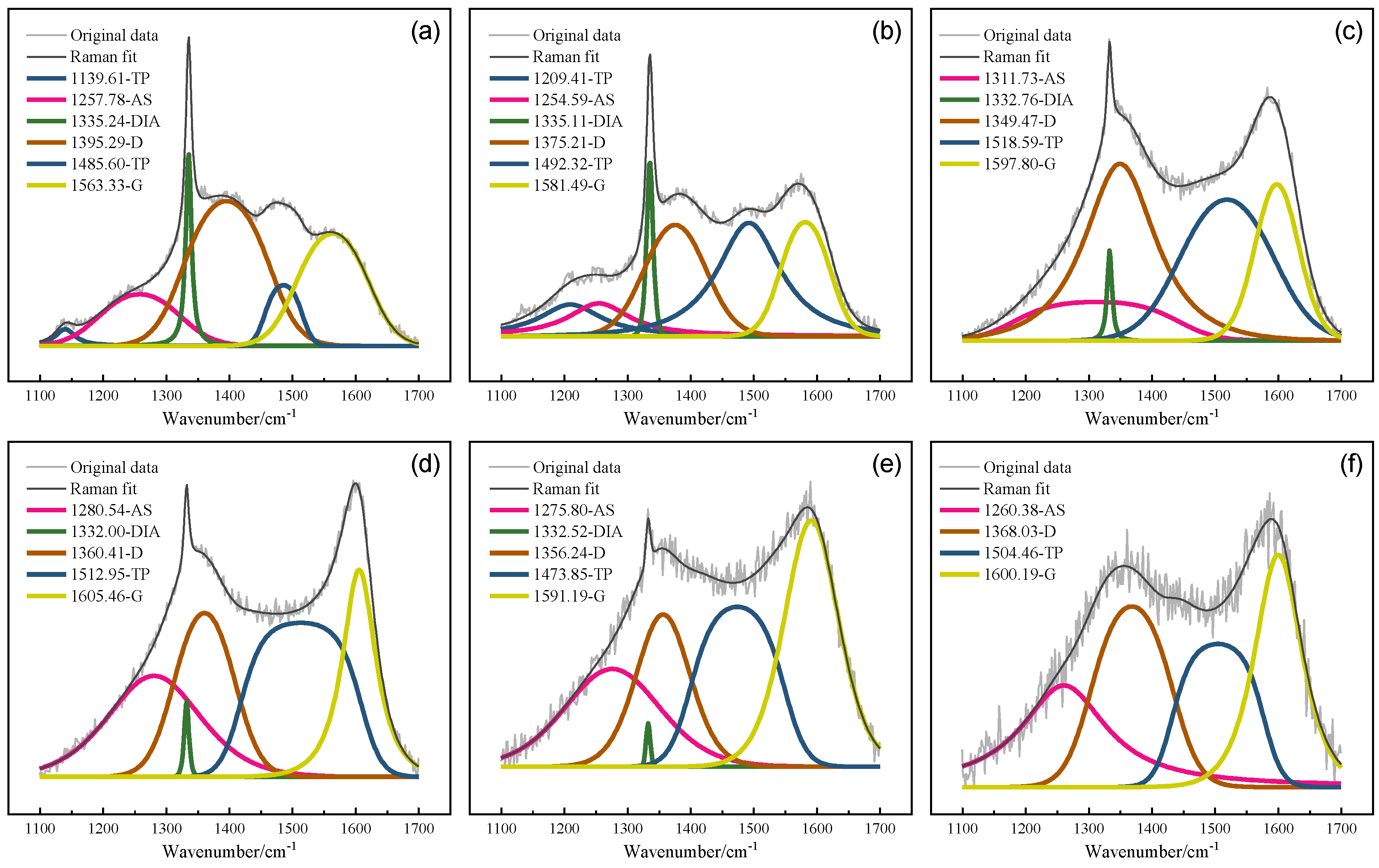
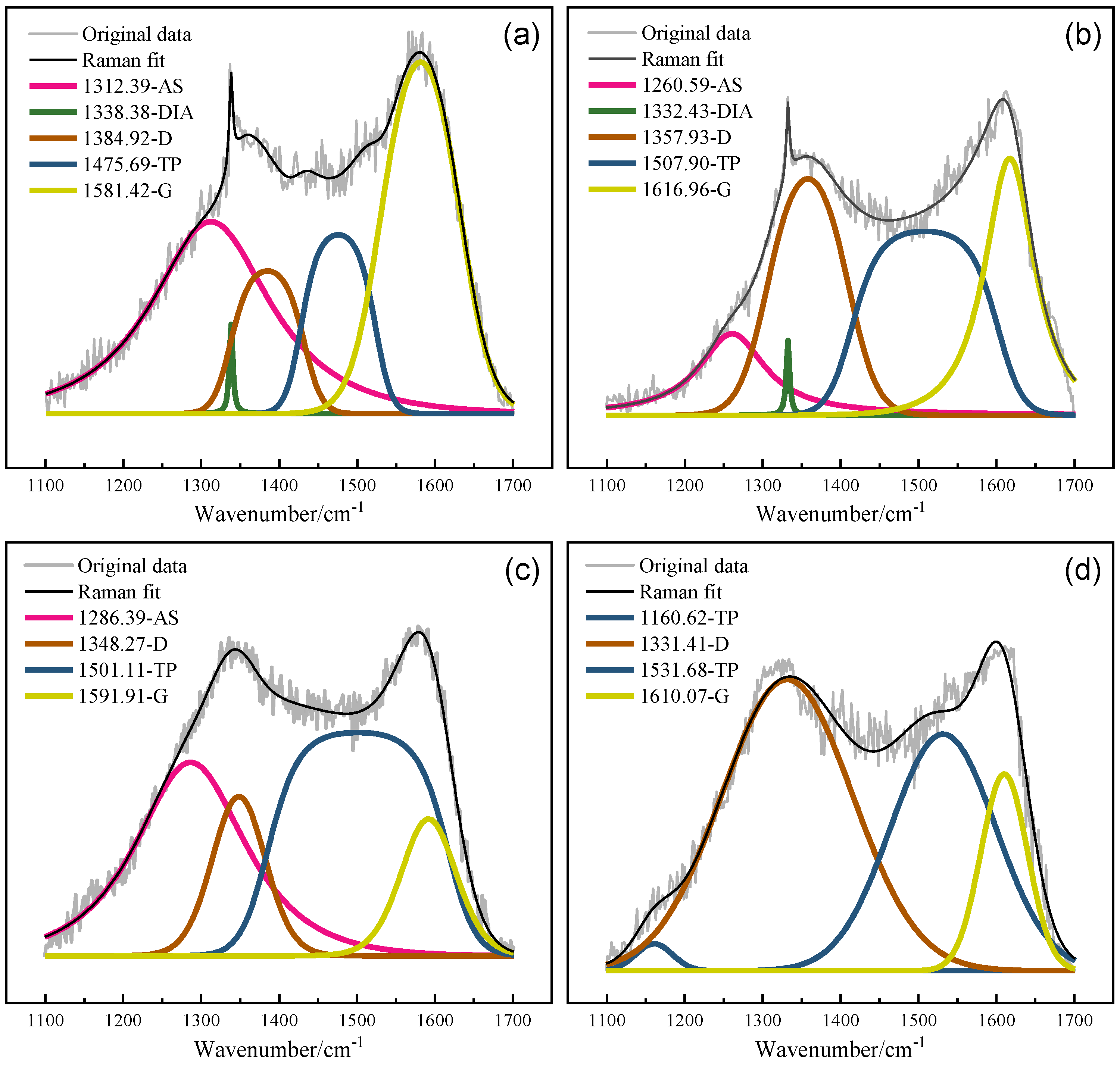
  • Concerning carbon phase transition, when withstanding harsh conditions (low scanning speed or high pulse energy), the diamond phase is weakened and disappears eventually when scanning speed decreases to 1.2 mm/s or pulse energy reaches 80 μJ. Another conclusion can be drawn from the shift pattern of diamond peaks that the compressive stress in the diamond coating can be released by fs laser irradiation.
  • In the investigation of the interaction mechanism, EUV exhibits acceptable reliability referring to surface roughness and carbon phase composition by embracing all three processing parameters. The significant rank in the MRR response is repetition rate > pulse energy > scanning speed, and the Ra response ratio follows repetition rate > scanning speed > pulse energy.
  • The calculated ablation threshold of CVD diamond coating at effective pulses of 90 is 0.138 J/cm2, which is much smaller than that of SCD or PCD.

Author Contributions

Conceptualization, Y.M.; methodology, Y.M., C.W.; validation, Y.H., Y.Z. and L.Y.; formal analysis, C.W., Y.H.; investigation, C.W., Y.Z.; resources, Y.M., X.C.; data curation, L.Y.; writing—original draft preparation, C.W.; writing—review and editing, Y.M., C.W.; visualization, C.W.; supervision, Y.M., X.C.; project administration, Y.M, X.C.; funding acquisition, Y.M., X.C.

Funding

This research was funded by the National Natural Science Foundation of China, grant number 51375011, and Natural Science Foundation of Anhui Province, grant number 1208085 ME63, 1908085 ME129, and Natural Science Foundation of Anhui Education Department, grant number KJ2015 A050, KJ2015 A013.

Conflicts of Interest

The authors declare no conflict of interest.

References

  1. Ogawa, Y.; Ota, M.; Nakamoto, K.; Fukaya, T.; Russell, M.; Zohdi, T.I.; Yamazaki, K.; Aoyama, H. A study on machining of binder-less polycrystalline diamond by femtosecond pulsed laser for fabrication of micro milling tools. Manuf. Technol. 2016, 65, 245–248. [Google Scholar] [CrossRef]
  2. Wang, X.C.; Wang, C.C.; Sun, F.H.; Shen, B. Fabrication, polishing and application of diamond coated compacting die with sector-shaped hole. Chin. Surf. Eng. 2016, 29, 75–82. [Google Scholar]
  3. Chandran, M.; Kumaran, C.R.; Dumpala, R.; Shanmugam, P.; Natarajan, R.; Bhattacharya, S.S.; Rao, M.R. Nanocrystalline diamond coatings on the interior of WC–Co dies for drawing carbon steel tubes: Enhancement of tube properties. Diam. Relat. Mater. 2014, 50, 33–37. [Google Scholar] [CrossRef]
  4. Luo, F.; Ong, W.; Guan, Y.; Li, F.; Sun, S.; Lim, G.C.; Hong, M. Study of micro/nanostructures formed by a nanosecond laser in gaseous environments for stainless steel surface coloring. Appl. Surf. Sci. 2015, 328, 405–409. [Google Scholar] [CrossRef]
  5. Oliveira, V.; Sharma, S.P.; De Moura, M.F.S.F.; Moreira, R.D.F.; Vilar, R. Surface treatment of CFRP composites using femtosecond laser radiation. Opt. Lasers Eng. 2017, 94, 37–43. [Google Scholar] [CrossRef]
  6. Ruja, M.A.; de Souza, G.M.; Finer, Y. Ultrashort-pulse laser as a surface treatment for bonding between zirconia and resin cement. Dent. Mater. 2019. [Google Scholar] [CrossRef]
  7. Naoki, Y.; Kenzo, M.; Junsuke, K. Control of tribological properties of diamond-like carbon films with femtosecond-laser-induced nanostructuring. Appl. Surf. Sci. 2008, 254, 2364–2368. [Google Scholar]
  8. Jia, X.; Dong, L.L. Fabrication of complex micro/nanopatterns on semiconductors by the multi-beam interference of femtosecond laser. Phys. Procedia 2014, 56, 1059–1065. [Google Scholar] [CrossRef]
  9. Chen, J.Y.; Jin, T.Y.; Tian, Y.J. Development of an ultrahard nanotwinned cBN micro tool for cutting hardened steel. Sci. China-Technol. Sci. 2016, 59, 876–881. [Google Scholar] [CrossRef]
  10. Yin, J.; Chen, G.; Xiong, B.; Zhu, Z.; Jin, M. Femtosecond pulsed laser fabrication of a novel SCD grinding tool with positive rake angle. Appl. Phys. A 2018, 124, 859. [Google Scholar] [CrossRef]
  11. Zavedeev, E.V.; Zilova, O.S.; Barinov, A.D.; Shupegin, M.L.; Arutyunyan, N.R.; Jaeggi, B.; Neuenschwander, B.; Pimenov, S.M. Femtosecond laser microstructuring of diamond-like nanocomposite films. Diam. Relat. Mater. 2017, 74, 45–52. [Google Scholar] [CrossRef]
  12. Chen, G.; Zhu, Z.; Yin, J.; Xiong, B. Experiment on ablation threshold of single crystal diamond produced by femtosecond laser processing. Chin. J. Lasers 2019, 46, 4. [Google Scholar]
  13. Pimenov, S.M.; Jaeggi, B.; Neuenschwander, B.; Zavedeev, E.V.; Zilova, O.S.; Shupegin, M.L. Femtosecond laser surface texturing of diamond-like nanocomoposite films to improve tribological properties in lubricated sliding. Diam. Relat. Mater. 2019, 93, 42–49. [Google Scholar] [CrossRef]
  14. Xiang, D.; Chen, Y.; Guo, Z.; Feng, H.; Wu, B.; Niu, X. Influence of textured diamond film on tribological properties of cemented carbide substrate. Int. J. Refract. Met. Hard Mater. 2019, 78, 303–309. [Google Scholar] [CrossRef]
  15. Sugihara, T.; Enomoto, T. Development of a cutting tool with a nano/micro-textured surface: Improvement of anti-adhesive effect by considering the texture patterns. Precis. Eng. 2009, 33, 425–429. [Google Scholar] [CrossRef]
  16. Sugihara, T.; Enomoto, T. Improving anti-adhesion in aluminum alloy cutting by micro stripe texture. Precis. Eng. 2012, 36, 229–237. [Google Scholar] [CrossRef]
  17. Sugihara, T.; Enomoto, T. Crater and flank wear resistance of cutting tools having micro textured surfaces. Precis. Eng. 2013, 37, 888–896. [Google Scholar] [CrossRef]
  18. Sugihara, T.; Tanakaa, H.; Enomoto, T. Development of novel cBN cutting tool for high speed machining of inconel 718 focusing on coolant behaviors. Procedia Manuf. 2017, 10, 436–442. [Google Scholar] [CrossRef]
  19. Sui, T.Y.; Cui, Y.X.; Lin, B.; Zhang, D.W. Influence of nanosecond laser processed surface textures on the triboliogical characteristics of diamond films sliding against zirconia bioceramic. Ceram. Int. 2018, 44, 23137–23144. [Google Scholar] [CrossRef]
  20. Zhao, J.H.; Li, C.H.; Xu, J.J.; Hao, Y.W.; Li, X.B. Surface modification of nanostructured ZnS by femtosecond laser pulsing. Appl. Surf. Sci. 2014, 293, 332–335. [Google Scholar] [CrossRef]
  21. Tsubaki, A.T.; Koten, M.A.; Lucis, M.J.; Zuhlke, C.; Ianno, N.; Shield, J.E.; Alexander, D.R. Formation of aggregated nanoparticle spheres through femtosecond laser surface processing. Appl. Surf. Sci. 2017, 419, 778–787. [Google Scholar] [CrossRef] [PubMed] [Green Version]
  22. Liang, J.; Liu, W.; Li, Y.; Luo, Z.; Pang, D. A model to predict the ablation width and calculate the ablation threshold of femtosecond laser. Appl. Surf. Sci. 2018, 456, 482–486. [Google Scholar] [CrossRef]
  23. Kononenko, T.V.; Pivovarov, P.A.; Khomich, A.A.; Khmelnitsky, R.A.; Plotnichenko, V.G.; Konov, V.I. Processing of polycrystalline diamond surface by IR laser pulses without interior damage. Opt. Laser Technol. 2019, 117, 87–93. [Google Scholar] [CrossRef]
  24. Chen, N.; Li, Z.; Wu, Y.; Zhao, G.; Li, L.; He, N. Investigating the ablation depth and surface roughness of laser-induced nano-ablation of CVD diamond material. Precis. Eng. J. Int. Soc. Precis. 2019, 57, 220–228. [Google Scholar] [CrossRef]
  25. Huang, J.H.; Liang, G.W.; Li, J.; Guo, B.P. Femtosecond Laser Processing of Polycrystalline Diamond Micro-Structure Array. Chin. J. Lasers 2017, 44, 105–111. [Google Scholar]
  26. Ohfuji, H.; Okuchi, T.; Odake, S.; Kagi, H.; Sumiya, H.; Irifune, T. Micro-/nanostructural investigation of laser-cut surfaces of single- and polycrystalline diamonds. Diam. Relat. Mater. 2010, 19, 1040–1051. [Google Scholar] [CrossRef]
  27. Granados, E.; Martinez-Calderon, M.; Gomez, M.; Rodriguez, A.; Olaizola, S.M. Photonic structures in diamond based on femtosecond UV laser induced periodic surface structuring (LIPSS). Opt. Express 2017, 25, 15330–15335. [Google Scholar] [CrossRef]
  28. Trucchi, D.M.; Orlando, S. Surface Texturing of CVD Diamond Assisted by Ultrashort Laser Pulses. Coatings 2017, 7, 185. [Google Scholar] [CrossRef]
  29. Sartori, A.F.; Orlando, S.; Bellucci, A.; Trucchi, D.M.; Abrahami, S.; Boehme, T.; Hantschel, T.; Vandervorst, W.; Buijnsters, J.G. Laser-Induced Periodic Surface Structures ( LIPSS ) on Heavily Boron- Doped Diamond for Electrode Applications. Appl. Mater. Interfaces 2018, 10, 43236–43251. [Google Scholar] [CrossRef]
  30. Sedao, X.; Lenci, M.; Rudenko, A.; Faure, N.; Pascale-Hamri, A.; Colombier, J.P.; Mauclair, C. Influence of pulse repetition rate on morphology and material removal rate of ultrafast laser ablated metallic surfaces. Opt. Lasers Eng. 2019, 116, 68–74. [Google Scholar] [CrossRef]
  31. Evlashin, S.A.; Svyakhovskiy, S.E.; Fedorov, F.S.; Mankelevich, Y.A.; Dyakonov, P.V.; Minaev, N.V.; Dagesyan, S.A.; Maslakov, K.I.; Khmelnitsky, R.A.; Suetin, N.V.; et al. Ambient Condition Production of High Quality Reduced Graphene Oxide. Adv. Mater. Interfaces 2018, 5, 1801180. [Google Scholar] [CrossRef]
  32. Forster, M.; Huber, C.; Armbruster, O.; Kalish, R.; Kautek, W. 50-nanometer femtosecond pulse laser induced periodic surface structures on nitrogen-doped diamond. Diam. Relat. Mater. 2017, 74, 114–118. [Google Scholar] [CrossRef]
  33. Materials, H.; Fang, S.; Klein, S. Surface structuring of polycrystalline diamond (PCD) using ultrashort pulse laser and the study of force conditions. Int. J. Refract. Met. 2019, 84, 105036. [Google Scholar]
Figure 1. Experimental materials and schemes. (a) Surface SEM photograph of the diamond coating; (b) three-dimensional topography and section profile(orange curve) of the coating; (c) schematic of the adopted femtosecond laser processing system; and (d) three experimental schemes, namely, changing the number of pulses N only, changing the single pulse energy E only, and changing both N and E.
Applsci 09 04273 g001
Figure 2. SEM photographs of fs laser-irradiated regions under different scanning speeds. (a) As-grown; (b) 2.0 mm/s; (c) 1.8 mm/s; (d) 1.6 mm/s; (e) 1.4 mm/s; and (f) 1.2 mm/s. The red arrow indicates the direction of laser polarization.
Applsci 09 04273 g002
Figure 3. White light (WL) interferometer reconstructed results of fs laser-irradiated regions under different scanning speeds. (a) 2.0 mm/s, (b) 1.8 mm/s, (c) 1.6 mm/s, (d) 1.4 mm/s, (e) 1.2 mm/s, and (f) the surface roughness Ra and removal rate per laser pulse of diamond coating vs. scanning speed.
Applsci 09 04273 g003
Figure 4. Raman spectra of the diamond coatings irradiated under different scanning speeds. (a) As-grown, (b) 2.0 mm/s, (c) 1.8 mm/s, (d) 1.6 mm/s, (e) 1.4 mm/s, and (f)1.2 mm/s.
Applsci 09 04273 g004
Figure 5. SEM photographs of fs laser-irradiated regions under different single pulse energies. (a) 50 μJ, (b) 70 μJ, (c) 80 μJ, and (d) 100 μJ. The red arrow indicates the direction of laser polarization.
Applsci 09 04273 g005
Figure 6. WL interferometer reconstructed results of fs laser-irradiated regions under different pulse energy. (a) 50 μJ, (b) 70 μJ, (c)80 μJ, and (d) 100 μJ.
Applsci 09 04273 g006
Figure 7. The surface roughness Ra and MRR vs. single pulse energies. The scanning speed is 1 mm/s, and the repetition rate is 1 kHz.
Applsci 09 04273 g007
Figure 8. Raman spectra of the diamond coatings irradiated under different pulse energies. (a) 50 μJ, (b) 70 μJ, (c) 80 μJ, and (d) 100 μJ.
Applsci 09 04273 g008
Figure 9. SEM photographs of fs laser-irradiated regions under the interaction of pulse energy and repetition rate. The scanning speed is 1 mm/s.
Applsci 09 04273 g009
Figure 10. WL interferometer reconstructed topographies of fs laser-irradiated regions under (a) 500 Hz × 200 μJ, (b)10 kHz × 10 μJ, and (c)100 kHz × 1 μJ. (d) Surface roughness Ra and MRR measured under the given conditions.
Applsci 09 04273 g010
Figure 11. Schematic diagram of fs laser direct writing to produce a single line, where l is the length of the single line, which is equal to the side length of the sample (10 mm), and V is the volume removed by fs laser ablation, which can be directly extracted from the WL interferometer results.
Applsci 09 04273 g011
Figure 12. Re-plotted curve based on the available data obtained in this work. (a) The relationship between the Ra and EUV image inserts shows the corresponding morphologies of EUV connected by a dotted line. (b) The correlation between Raman peak position and EUV.
Applsci 09 04273 g012
Figure 13. Responses for the S/N of Ra and MRR measurements. The significant rank in the MRR response is f > E > v, the Ra response ratio follows f > v > E.
Applsci 09 04273 g013
Figure 14. Schematic diagram of femtosecond laser energy distribution. The threshold of the target is equivalent to the laser fluence distributed at the border of the effective ablation region.
Applsci 09 04273 g014
Figure 15. Scatter plot of the square of ablation width against the logarithm of laser power. The red line is the linear fitting of the plot, the fitting function is shown in the upper left.
Applsci 09 04273 g015
Table 1. Preparation conditions of CVD diamond film.
ConditionsDeposition Parameters
Flow of Acetone/Hydrogen30/300 sccm
Pressure5 kPa
The voltage of Tantalum wire20 V
Bias current2 A
Distance between Tantalum wire and substrate9–10 mm
Deposition temperature450 °C
The time of deposition3 h
Table 2. The processing parameters applied for fs laser etching.
Fixed ParametersControlled Parameters
Wavelength/nmPulse duration/fsSpeed/mm.s−1Pulse energy/μJRepetition rate/Hz
8001001.2–2.050–100500–100 K
Table 3. Experimental parameters and their corresponding EUV (energies applied to unit volume).
Experimental ConditionEUV (μJ/μm3)Experimental ConditionEUV (μJ/μm3)Experimental ConditionEUV (μJ/μm3)
2 mm/s0.572350 μJ0.4886500 Hz × 200 μJ0.858
1.8 mm/s0.607170 μJ0.663110 kHz × 10 μJ0.8265
1.6 mm/s0.657380 μJ0.6709100 kHz × 1 μJ0.8475
1.4 mm/s0.6785100 μJ0.8464
1.2 mm/s0.7873
Table 4. Process parameters and design levels used in the L16(43) Taguchi array.
FactorsSymbolUnitLevel 1Level 2Level 3Level 4
Scanning speedvmm/s1102050
Pulse energyEμJ1050100120
Repetition ratefHz10050010002000

