Next Article in Journal
Expert Finding Systems: A Systematic Review
Next Article in Special Issue
Development of a Comprehensive Model for the Coulombic Efficiency and Capacity Fade of LiFePO4 Batteries under Different Aging Conditions
Previous Article in Journal
Fault Inference of Electronic Equipment Based on Multi-State Fuzzy Bayesian Network
Previous Article in Special Issue
SOC Estimation with an Adaptive Unscented Kalman Filter Based on Model Parameter Optimization
 
 
Erratum published on 30 December 2020, see Appl. Sci. 2021, 11(1), 276.
Article

Small-Signal Modeling and Analysis for a Wirelessly Distributed and Enabled Battery Energy Storage System of Electric Vehicles

Department of Electrical and Computer Engineering, College of Engineering, The University of Alabama, Tuscaloosa, AL 35487, USA
*
Author to whom correspondence should be addressed.
Appl. Sci. 2019, 9(20), 4249; https://doi.org/10.3390/app9204249
Submission received: 31 August 2019 / Revised: 1 October 2019 / Accepted: 7 October 2019 / Published: 11 October 2019
(This article belongs to the Special Issue Battery Management System for Future Electric Vehicles)

Abstract

:

Featured Application

The major object of this research is to provide a small-signal modeling method and controller design guidelines in wireless distributed and enabled battery energy storage system (WEDES) battery system for electric vehicles applications.

Abstract

This paper presents small-signal modeling, analysis, and control design for wireless distributed and enabled battery energy storage system (WEDES) for electric vehicles (EVs), which can realize the active state-of-charge (SOC) balancing between each WEDES battery module and maintain operation with a regulated bus voltage. The derived small-signal models of the WEDES system consist of several sub-models, such as the DC-DC boost converter model, wireless power transfer model, and the models of control compensators. The small-signal models are able to provide deep insight analysis of the steady-state and dynamics of the WEDES battery system and provide design guidelines or criteria of the WEDES controller. The derived small-signal models and controller design are evaluated and validated by both MATLAB®/SIMULINK simulation and hardware experimental prototype.

1. Introduction

Battery energy storage systems (BESS) have been widely used in various applications, such as electric vehicles (EVs), consumer electronics, medical devices, smart grid, energy backup in data centers, and among others [1,2,3,4,5,6,7,8,9,10]. For EV applications, what is referred to be as “range anxiety” is one of the major reasons that prohibit or slows down the adoption of EVs [9,10,11,12,13,14].
To eliminate range anxiety in and extend the driving range of EVs, different methods have been discussed in the literature [9,10,11,12,13,14,15,16,17], such as increasing battery pack capacity, utilizing a faster charging method, utilizing a battery pack swapping method, achieving dynamic wireless charging, etc. While these methods can be effective to extend the driving range of EVs, some design challenges or drawbacks cannot be ignored.
When increasing capacity, the weight, size, and cost of the battery pack inevitably increase with the increase in battery capacity [10]. Further, the needed recharge time is also increased. For faster charging, the battery state-of-health (SOH) degrades at a higher rate if faster charging is applied [11,12]. In addition, the fast charger requires a high-power infrastructure that increases the cost of the overall system. For conventional battery swapping, specialized equipment, as well as the experienced personnel, are required to realize battery swapping [13]. For dynamic wireless charging, a large number of transmitter (Tx) coils are required with corresponding power supply units, which increases the infrastructure cost. In addition, this method might not be practical in all locations [14].
Among these methods, the battery swapping concept is a good candidate to reduce recharging time and extend the driving range with low infrastructure cost. To deal with the challenges in the conventional battery swapping concept, a new distributed and enabled battery energy storage (WEDES) system and WEDES controller for EVs are presented in [1], which allows for fast and safe exchange/swapping of smaller and lighter battery modules with wireless power transfer (WPT) technology [18,19].
An illustration of the WEDES system for EVs is shown in Figure 1b, and its example circuit diagram is shown in Figure 1c. Each of the battery modules consists of multiple battery cells, a dedicated electronics circuit, wireless power transmitter coil (Tx coil), wireless communication circuit, and client controller. While the on-board-unit (OBU) consists of a wireless power receiver coil (Rx coil), wireless communication circuit, and host controller. Different from the conventional battery swapping concept where the battery pack as a whole is exchanged at one time, in the WEDES battery system, the conventional single battery pack is divided into multiple small battery modules, which can deliver power through wireless power transfer (WPT) technology to the OBU. The distributed nature of the WEDES system combined with wireless power transfer (no physical connection between battery modules and OBU) makes the battery exchange/swapping easier, safer, and faster.
The distributed WEDES battery system with the WEDES controller addresses state-of-charge (SOC) balancing, bus voltage regulation, and battery module current/voltage regulation at the same time inside the system. Therefore, an SOC balancing control loop, a bus voltage regulation control loop, and a battery module current/voltage control loop are coupled with each other within one battery module as well as between multiple battery modules. These couplings make the analysis and design of the WEDES controller complex and critical. While the initial concept of the distributed WEDES battery system is discussed in [1], the small-signal modeling and controller design analysis are not focused on.
The main contributions of this paper can be summarized as follows:
(1).
The overall review of the wireless distributed WEDES system, which allows for fast and safe exchange/swapping of battery modules when utilized in electric vehicles (EVs) applications to deal with the range anxiety issue.
(2).
The derivation of small-signal modeling of the WEDES battery system to comprehensively analyze the steady-state stability and dynamic response of the WEDES battery system.
(3).
The discussion of the guidelines for the controller design of multiple interacted control loops.
(4).
The discussion of the simulation results and hardware experimental results to evaluate and validate the accuracy and effectiveness of the derived small-signal model and designed compensators.
The next Section discusses the detailed small-signal derivation of the WEDES system. Section 3 presents the design of compensators for each control loop. Simulation models and experimental results are presented and discussed in Section 4 to validate the derived small-signal models. Section 5 is the additional comments, and Section 6 concludes the paper.

2. Small-Signal Modeling of the Distributed WEDES System

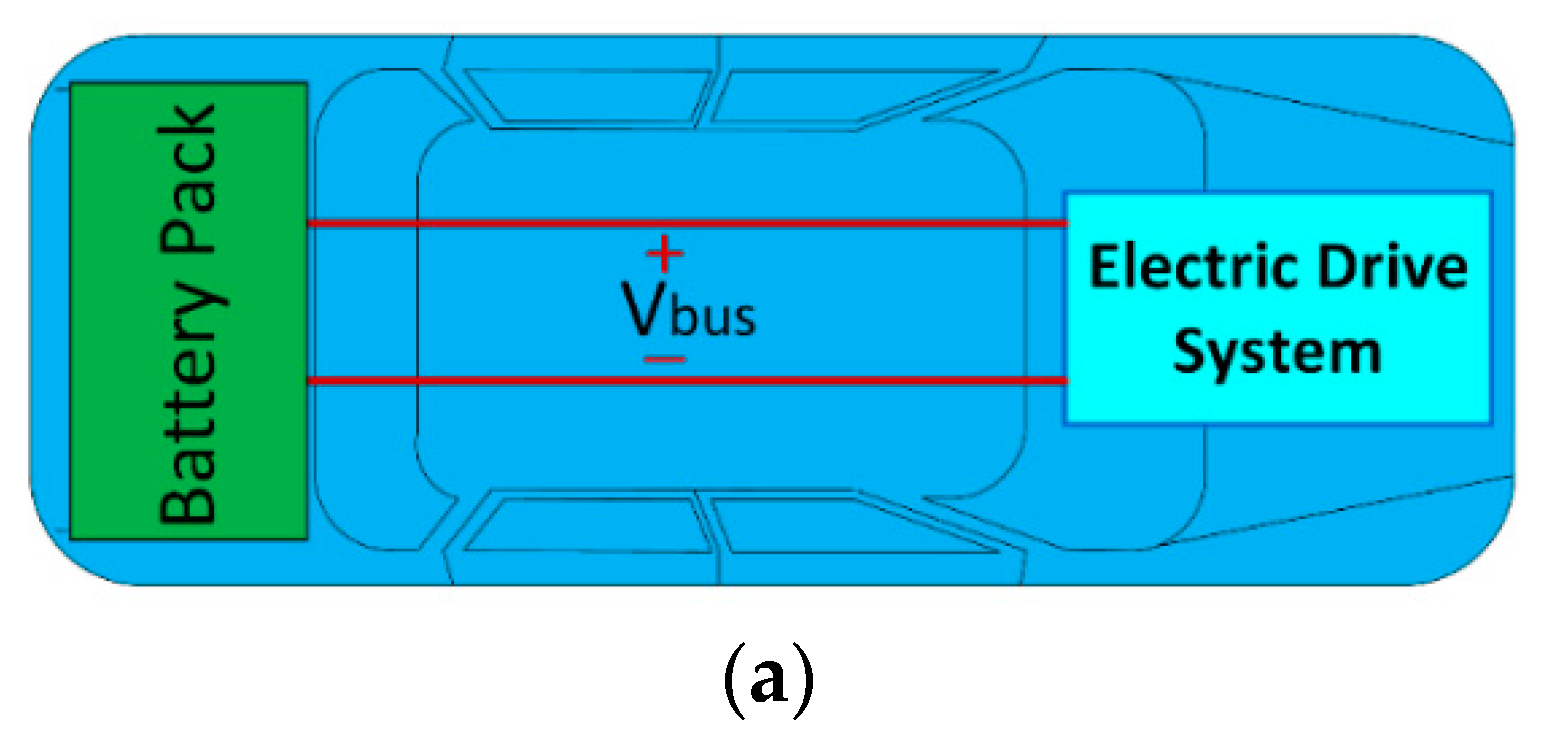
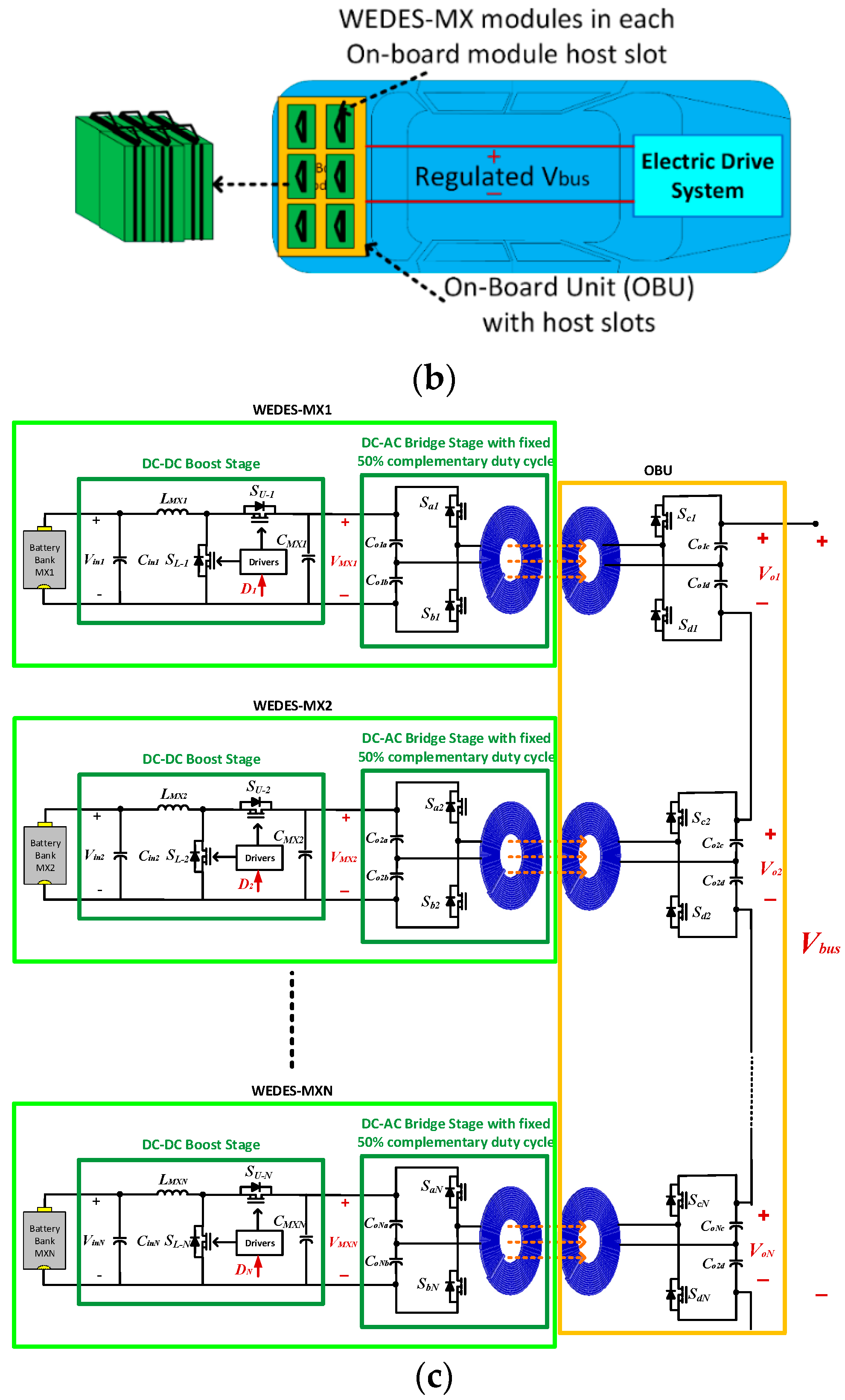
2.1. Overview of the WEDES System and Controller Operation Principle

Figure 1c shows the illustration of an example circuit diagram of the WEDES system, which consists of two major parts: battery modules and on-board-unit (OBU).
Inside each battery module, multiple battery cells are connected in series and/or in parallel to form a battery bank, which can provide voltage/current/power to the rest of the system. The output of the battery bank is then connected to the input of a DC-DC power converter, which is used to achieve bus voltage regulation, battery module current/voltage regulation as well as SOC balancing at the same time as described later in this section. The output of the power converter is connected to an inverter stage for DC-AC power conversion. At the end of the battery module, the AC power from the inverter is applied to the transmitter (Tx) for inductive wireless power transfer (I-WPT) to the OBU.
The OBU mainly consists of receiver coils (Rx) followed by an AC-DC power conversion/rectification stage (rectifier). The outputs of each rectifier (Vo1 through VoN) are connected in series to the bus/output (Vbus = Vo1 + Vo2 + … + VoN).
To realize the functionalities of SOC balancing, bus voltage regulation, and battery module current/voltage regulation, the WEDES controller consists of three different control loops: the SOC balancing control loop (referred to be by the SOC balancing loop), battery module voltage control loop (referred to be by the module voltage loop) and bus voltage control loop (referred to be by the bus voltage loop). Figure 2 shows the diagram of the wirelessly distributed WEDES controller, where Vbus_ref is the desired value of bus voltage, VMN-total is an intermediate value for voltage regulation, C_re_MX1 though C_re_MXN are the remaining capacities of battery modules for SOC calculation, SOCMX1 though SOCMXN are the SOC values of battery modules, λDC1 through λDCN are weighting factors to generate the reference values of VMX1-DC-ref through VMXN-DC-ref for each battery module, αMX1 through αMXN are the SOC multipliers and δMX1 through δMXN are enable/disable values.
In the WEDES controller, the SOC balancing loop is used to generate multipliers αMX1 through αMXN to realize SOC balancing between multiple battery modules, as given by Equation (1).
{ α M X 1 =   ( S O C M X r e f S O C M X 1 ) × G v S O C + 1 α M X 2 =   ( S O C M X r e f S O C M X 2 ) × G v S O C + 1 . α M X N =   ( S O C M X r e f S O C M X N ) × G v S O C + 1 ,
where SOCMX-ref is the average SOC value of all battery modules, as given by Equation (2). When all battery modules are inserted and active, the sum of all δMX1 through δMXN equals to N ( δ M X 1 +   δ M X 2 + + δ M X N   = N).
S O C M X r e f   =   ( δ M X 1 × S O C M X 1 ) + ( δ M X 2 ×   S O C M X 2 ) + +   ( δ M X N × S O C M X N ) δ M X 1 +   δ M X 2 + + δ M X N   ,
λ D C r =   δ M X r   ×   α M X r ( δ M X 1   ×   α M X 1 ) +   ( δ M X 2   ×   α M X 2 ) + +   ( δ M X N   ×   α M X N )
If the SOC value of rth battery module is larger than others, the corresponding multiplier αMXr will be set larger, and vice versa. These multipliers αMX1 through αMXN are then multiplied by enabled/disable values δMX1 through δMXN to further generate the weighting factors λDC1 through λDCN, as given by Equation (3). The sum of weighting factors λDC1 through λDCN always equals to one. These weighting factors are then used in the battery module voltage loop to regulate the output voltage of the battery modules VMX1 through VMXN at the primary side (Tx side), and as a result, achieve bus voltage regulation at the second side (Rx/OBU side).
It should be emphasized that due to the inevitable power loss during wireless power transfer (i.e., transmission efficiency is less than 100%), the bus voltage control loop is important to adaptively adjust VMN-total value to compensate the conversion ratios and losses of multiple power conversion stages (DC-AC-AC-DC) and realize bus voltage regulation. The relationship between different voltages can be calculated as given by Equation (4).
{ V M X t o t a l = ( V b u s r e f V b u s ) × G v b u s V M X t o t a l =   V M X 1 +   V M X 2 + + V M X N V M X r D C r e f = V M X t o t a l × λ D C r V b u s =   V o 1 +   V o 2 + + V o N              
To summarize, the presented WEDES controller can dynamically control SOC multipliers αMX1 through αMXN to adjust the discharging rate for each battery module to achieve SOC balancing, while keeping λDC1 + λDC2+…+λDCN = 1 such that the bus voltage is always regulated as Vbus-ref.

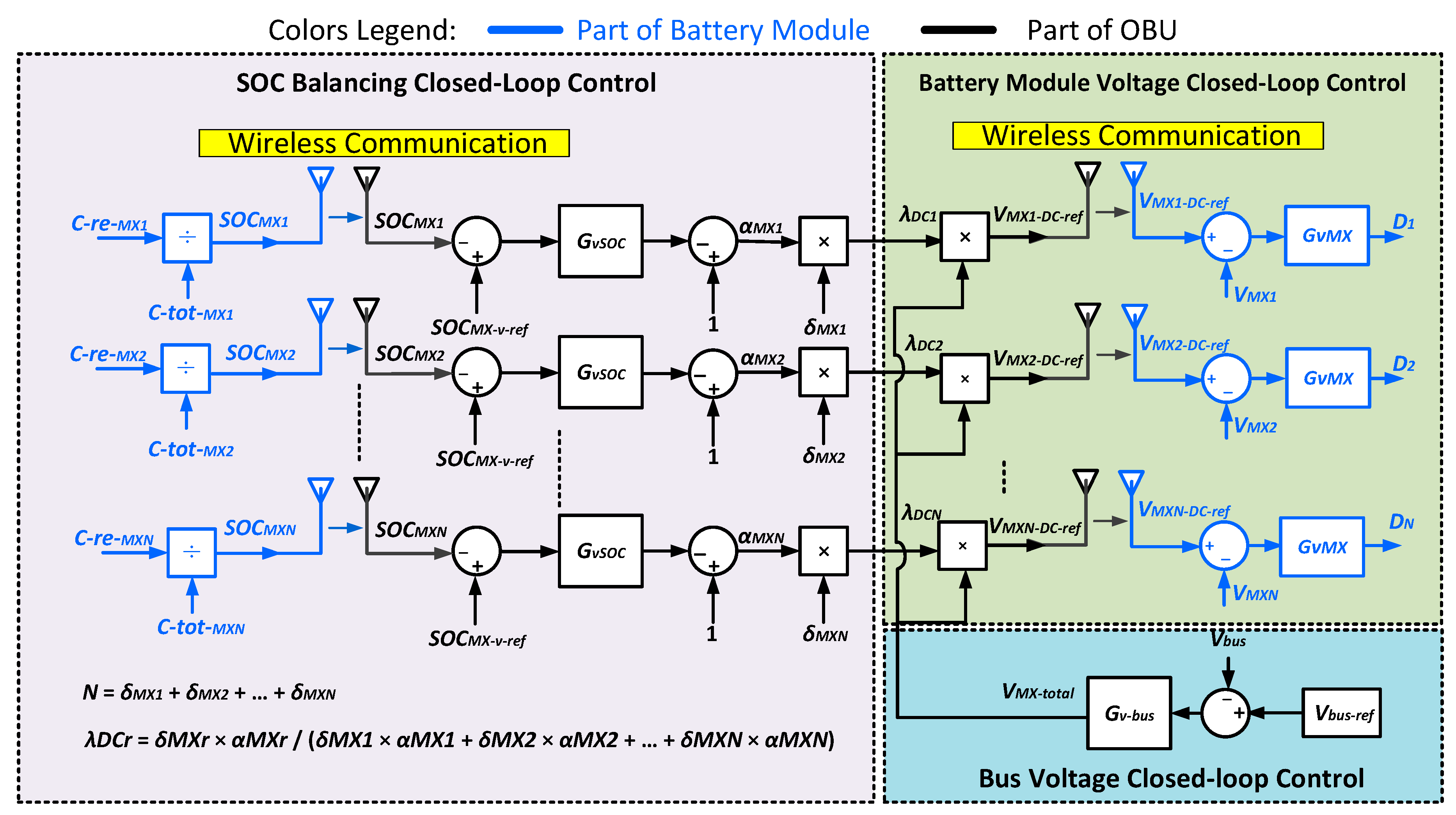
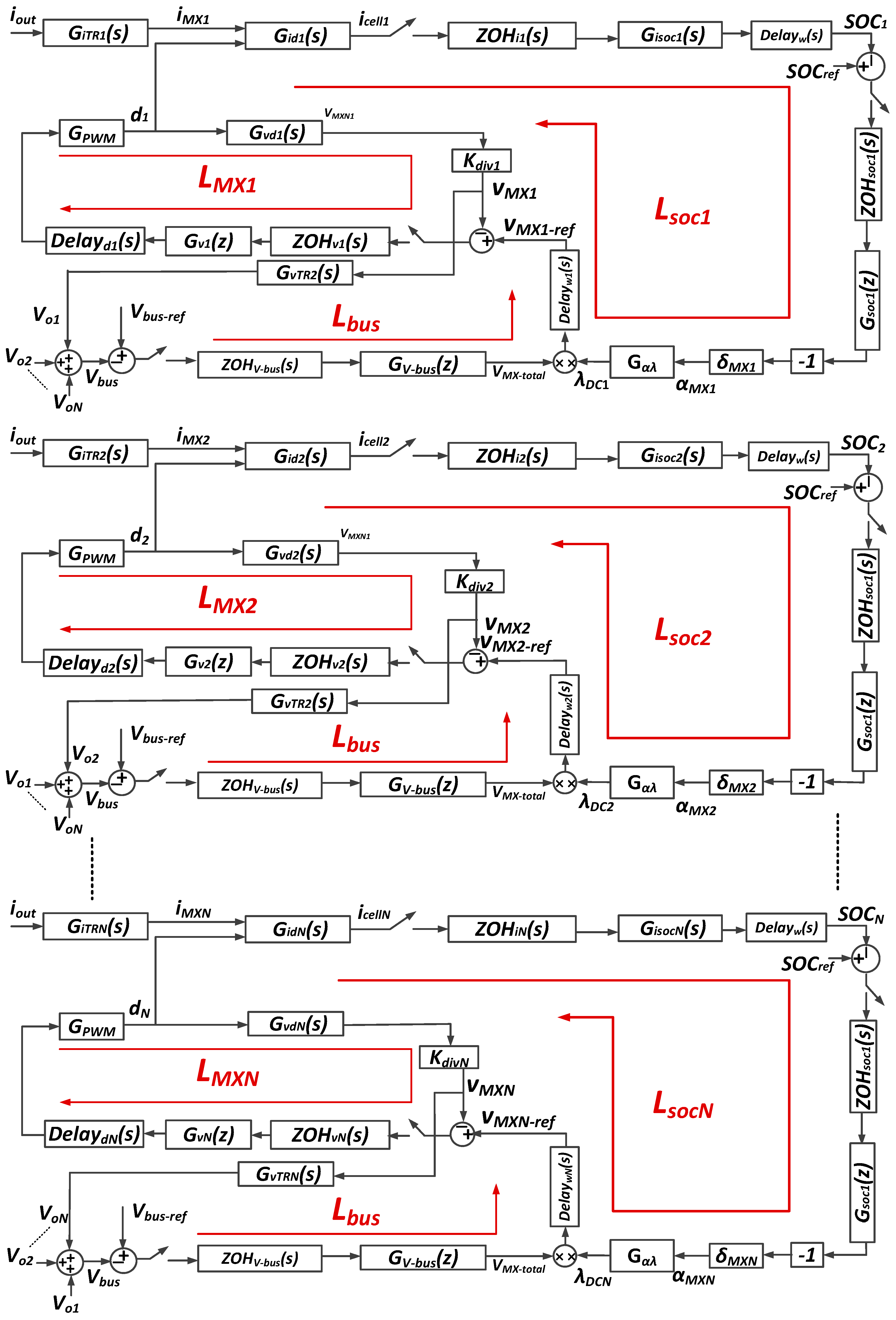
2.2. Small-signal Modeling

Based on the block diagram of the WEDES controller shown in Figure 2, the small-signal of the distributed WEDES system with controller is shown in Figure 3. The transfer functions and symbols in Figure 3 are summarized as follows. For simplicity, the rth battery module is used for illustration.
  • L b u s ( s ) : Bus voltage control loop gain;
  • L M X r ( s ) : Battery module voltage control loop gain;
  • L S O C r ( s ) : SOC balancing control loop gain;
  • G v d r ( s ) : Duty cycle to DC-DC converter output voltage VMXN transfer function;
  • G i d N ( s ) : Duty cycle to cell current transfer function;
  • G s o c i r ( s ) : Cell current to cell SOC transfer function;
  • G i T R ( s ) : Gain of the input current of the half-bridge inverter to the output current of rectifier;
  • G v T R ( s ) : Gain of the input voltage of the half-bridge inverter to the output voltage of rectifier;
  • G P W M : PWM module gain;
  • K d i v r ( s ) : Output voltage sensing gain (including voltage divider gain and ADC conversion gain);
  • D e l a y w r ( s ) : Delay of wireless communication;
  • D e l a y d r ( s ) : Delay of digital computation;
  • Z O H v r ( s ) : Zero order hold model of voltage sampling;
  • Z O H i r ( s ) : Zero order hold model of current sampling;
  • Z O H S O C r ( s ) : Zero order hold model of SOC sampling.

2.3. Derivation of Transfer Functions

Since the design parameters and equilibrium operation point of all WEDES battery modules are the same under steady-state operation (when SOC balancing is achieved), the derivation of transfer functions of all battery modules follows the same procedure. The detailed derivation of rth battery module is discussed as follows:

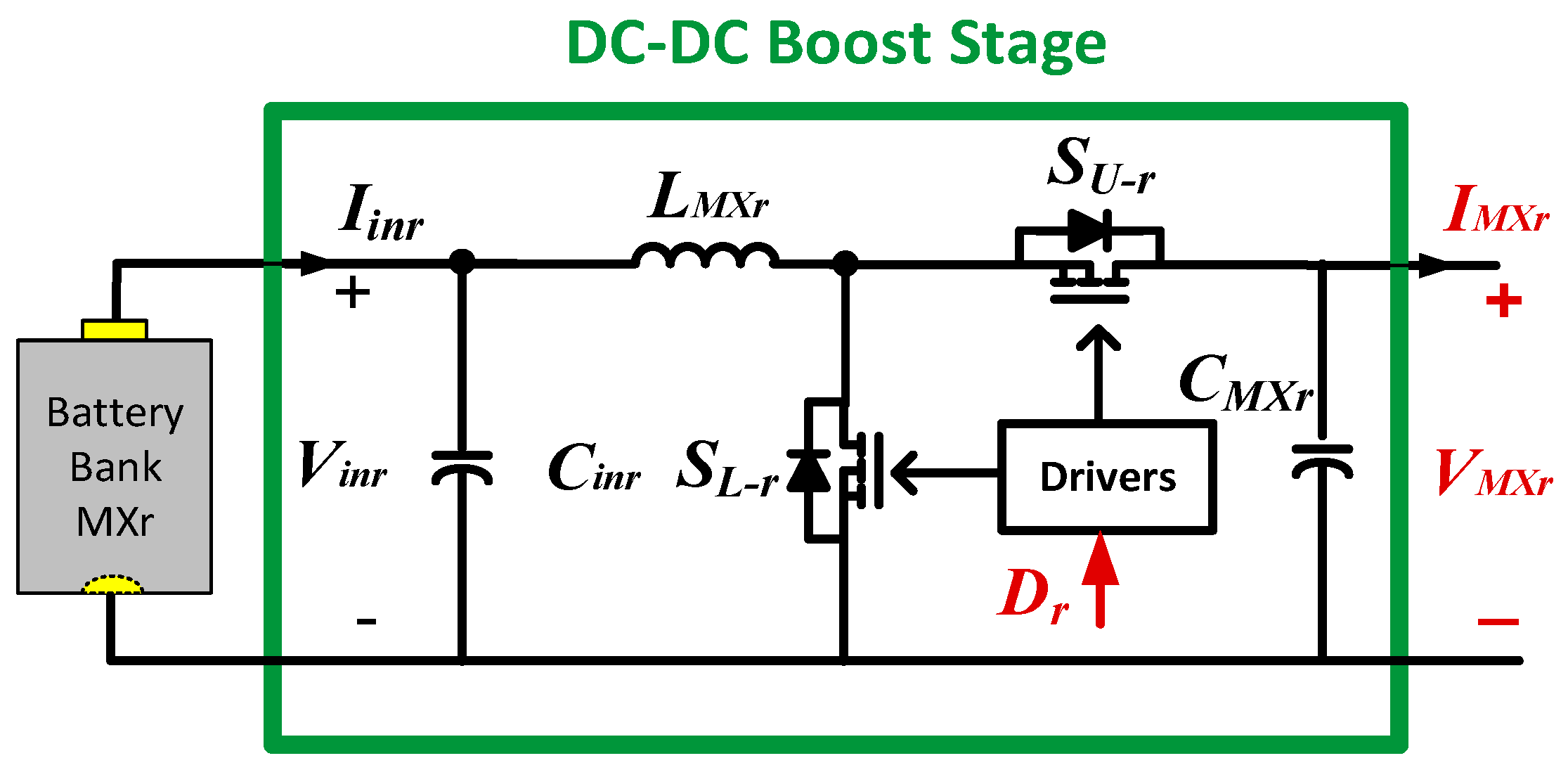
2.3.1. Transfer Function of DC-DC Boost Stage

The circuit diagram of the DC-DC boost stage is shown in Figure 4. When the lower side switch SL-r is on and the upper side switch SU-r is off, the differential equation of the boost converter can be derived as follows:
{ L M X r d i i n r d t = v i n r C M X r d v M X r d t = i M X r ,
where i i n r and v i n r are the input current and input voltage, respectively, and i M X r and v M X r are the output current and output voltage of the boost converter, respectively. LMXr is the inductor value, and CMXr is the output capacitor.
The state-space form of Equation (5) can be rewritten as Equation (6).
K [ x 1 ˙ x 2 ˙ ] = A 1 [ x 1 x 2 ] + B 1 [ u 1 u 2 ] = [ 0 0 0 0 ] [ x 1 x 2 ] + [ 1 0 0 1 ] [ u 1 u 2 ] .   ,
where the variables are x 1 = i i n r , x 2 = v M X r , u 1 = v i n r , u 2 = i M X r , respectively. K = [ L 0 0 C ] .
Similarly, when the lower side switch SL-r is off and the upper side switch SU-r is on, the differential equation of the boost converter can be derived as follows:
{ L M X r d i i n r d t = V i n r V M X r C M X r d V M X r d t = i i n r I M X r .
The state-space form of Equation (7) can be rewritten as Equation (8).
K [ x 1 ˙ x 2 ˙ ] = A 2 [ x 1 x 2 ] + B 2 [ u 1 u 2 ] = [ 0 1 1 0 ] [ x 1 x 2 ] + [ 1 0 0 1 ] [ u 1 u 2 ]
By using the state-space averaging method [20], the average matrix A and B are calculated as given by Equations (9) and (10).
A = A 1 D r + A 2 ( 1 D r ) ,
B = B 1 D r + B 2 ( 1 D r ) ,
where Dr is the duty cycle of the boost converter.
The steady-state X is calculated as follows:
X = A 1 B U = [ I M X r 1 D r V i n r ] 1 .
The small-signal equation becomes as given by Equation (12):
X ^ = A x ^ + B u ^ + [ ( A 1 A 2 ) X + ( B 1 B 2 ) U ] d r , ^
where A 1 A 2 = [ 0 1 1 0 ] , B 1 B 2 = 0 , and d r ^ is the small signal variation of duty cycle around its steady state operation point.
Equation (12) can be rewritten as Equation (13):
{ L M X r d i i n r ^ d t = ( 1 D r ) v M X r + v i n r ^ + V i n r 1 D r d r ^ C M X r d V M X r ^ d t = ( 1 D r ) i i n r ^ i M X r ^ I M X r 1 D r d r ^ .
To simply the analysis, the AC small-signal variation of v i n N ^ and i M X N ^ is assumed to be 0 (negligible) because the dynamic variation of battery voltage and battery module output current is very slow compared to the dynamic variation of the control signal d r ^ (duty cycle) of the power converter. Therefore, by performing the Laplace transformation, Equation (14) can be derived as:
{ s L M X r i i n r ( s ) = ( 1 D r ) v M X r ( s ) + V i n r 1 D r d r ( s ) s C M X r v M X r ( s ) = ( 1 D r ) i i n r ( s ) I M X N 1 D r d r ( s ) .
Based on Equation (15), the output voltage to the control signal transfer function of the power converter can be derived as
G v d r = v M X r ( s ) d r ( s ) = 1 C M X r ( I M X r 1 D r s + V i n r C M X r ) s 2 + ( 1 D r ) 2 L M X r C M X r .
Similarly, the input current to control signal transfer function can be derived as
G i d r = i i n r ( s ) d r ( s ) = 1 L M X r ( I M X r C M X r + V i n r 1 D r s ) s 2 + ( 1 D r ) 2 L M X r C M X r .

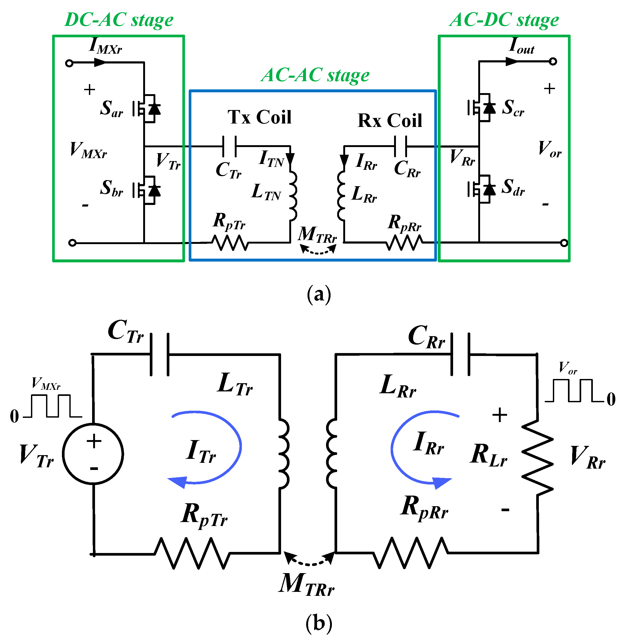
2.3.2. Transfer Function of WPT Stage (Half-Bridge Inverter, WPT Coils, and Half-Bridge Rectifier)

Figure 5 shows the circuit diagram of the WPT stage. By writing the Kirchhoff’s voltage law (KVL) equations as given by Equation (17), the ratio between the output voltage VRr and the input voltage VTr at the resonance frequency can be calculated as given by Equation (18).
[ j ω L T r + 1 j ω C T r + R p T r j ω M T R j ω M T R j ω L R r + 1 j ω C R r + R p T r + R L r ] [ I T r I R r ] = [ V T r 0 ] ,
      G v T R r | ω = ω o = V R r V T r = j ω M T R r R L r Z T r Z R r + ( ω M T R ) 2 = j ω k T R r L T r L R r R L r Z T r Z R r + ( ω k T R r ) 2 L T r L R r ,
where Z T r = j ω L T r + 1 j ω C T r + R p T r is the equivalent impedance of Tx side and Z R r = j ω L R r + 1 j ω C R r + R p T r + R L r is the equivalent impedance of Tx side. By substituting s = j ω into Equation (19), the following transfer function can be obtained.
G v T R r ( s ) = V R r ( s ) V T r ( s ) = s k T R r L T r L R r R L r Z T r Z R r + s 2 k T R r 2 L T r L R r .
Similarly, the ratio between the Tx current and Rx current can be derived as given by Equation (20).
G i T R r ( s ) = I R r ( s ) I T r ( s ) = s 2 k T R r C R r L T r L R r s 2 L R r C R r + s C R r ( R p T r + R L r ) + 1 .

3. Compensator Design

3.1. Battery Module Voltage Control Loop Compensator Design

The WEDES system design parameters are shown in Table 1. Based on the small-signal model in Figure 3, the uncompensated discrete-time transfer function of the battery module voltage loop for the rth battery module Gbusr (Z) consists of GPWM, Gvdr, GvTRr, kdivr, ZOHvr, and digital computation delay Delaydr. GbusN (Z) is calculated as given by Equation (21), and its bode plot is shown as the dashed curve in Figure 6.
L M X r u n c o m p ( z ) = Z { G P W M ( s ) · G v d r ( s ) · G v T R r ( s ) · Z O H v N ( s ) · D e l a y d N } =   0.0001999 z 0.000272 z 3 1.977 z 2 + 0.9789 z ,
where Z O H v r ( s ) = 1 e s · T s s   ; D e l a y d r ( s ) = e s T d e l a y ; T d e l a y is the digital controller computation delay and it is equal to 10 µs in the experimental implementation; G P W M =   1 / 1024   ; K d i v = 11 with 1 kΩ and 10 kΩ resistors as the voltage divider.
In the battery module voltage compensator design, there is a right-hand-plane-zero (RHPZ), which is located at 4.86 kHz. This RHPZ is introduced due to the existing boost converter. To guarantee the stability of the system, the compensated control bandwidth should be smaller than RHPZ. With a compensator Gv-bus(z) given by (22), the compensated battery module output voltage control loop gain ( G M X r _ c o m p = G M X r _ u n c o m p (z)⋅ G M X r ( z ) ) achieves a control bandwidth of 1.62 kHz and a phase margin of 45°, as shown on the solid curve in Figure 6.
  G M X r ( z ) = 950.8 z 2 1850 z + 899.7 z 2 z

3.2. SOC Balancing Loop Compensator Design

According to the small-signal model shown in Figure 3, the uncompensated SOC loop gain (i.e., with unity SOC loop compensator gain) is given by Equation (23), and its bode plot is represented by the dashed curve in Figure 7.
L s o c r u n c o m p ( z ) = Z { G i d N ( s ) · Z O H i c e l l N ( s ) · G s o c i N ( s ) · Z O H s o c N ( s ) · G s o c N · ( 1 ) · δ M X N · G α λ · D e l a y w · G v b u s } ,
where Z O H i c e l l N ( s ) =   1 e s · T s s   , Z O H s o c N ( s ) =   1 e s · T s o c s , Tsoc is the sampling period for the SOC value in the SOC balancing loop. Since the SOC value of a battery cell varies very slowly compared to the switching period of the power converter, the sampling rate of the SOC balancing loop does not have to be very fast. Tsoc =1 s is found to be a good trade-off between the hardware resource consumption, system stability and SOC balancing speed.
With a compensator given by Equation (24), the compensated SOC balancing loop gain achieves a control bandwidth of 0.057 Hz and phase margin of 59.2°, as shown on the solid curve in Figure 7. Due to the slow sampling rate of SOC value (1 Hz), it is expected that the control bandwidth of the SOC balancing loop is much lower than that of the voltage control loop.
  G S O C r ( z ) =   2.5 × 10 8 z 1

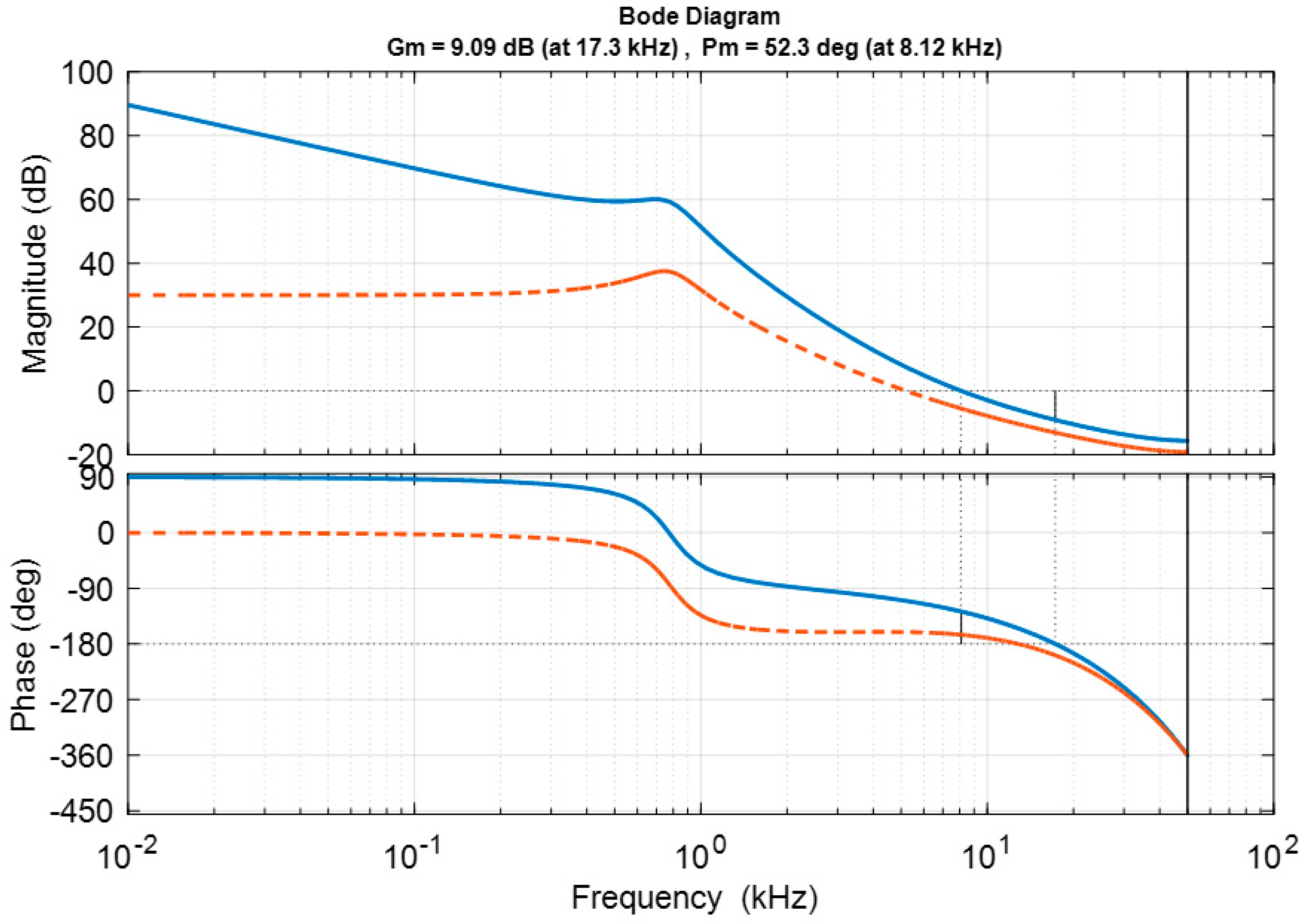
3.3. Bus Voltage Control Loop Compensator Design

Based on the small-signal model shown in Figure 3, the uncompensated bus voltage control loop gain (i.e., with gain = 1) is given by Equation (25), and its bode plot is represented by the dashed curve in Figure 8. With a compensator given by Equation (26), the compensated bus voltage loop gain achieves a control bandwidth of 8.12 kHz and a phase margin of 52.3°, as shown on the solid curve in Figure 8.
L b u s u n c o m p ( z ) = Z { Z O H v b u s ( s ) · D e l a y w } = 0.2555 z 0.1798 z 2 1.977 z + 0.9789 ,
G b u s ( z ) =   1.2 z 1.8 z 1 ,
where Z O H v b u s ( s ) =   1 e s · T s s .

4. Simulation and Model Experiment Validation

In this section, the small-signal model was evaluated and validated in both simulation and hardware experiments. The simulation model was built in MATLAB®/SIMULINK software (2018a, MatchWorks, Natick, Massachusetts, USA) using the derived transfer functions in Section 2 and Section 3. The hardware control compensator was implemented with Texas Instrumental microcontroller TMS320S28335. The design parameters are shown in Table 1. In the hardware experiment, three WEDES battery modules were implemented and utilized.
For the verification of derived small-signal models of the WEDES system, the dynamic response of both simulation and hardware experiments under different operation conditions was compared. If the dynamic performance from simulation results and experimental results are in good agreement, it can be implied that the developed model is valid.
As discussed in previous sections, there are three different control loops (battery module voltage control loop, bus voltage control loop, and SOC balancing control loop) in the WEDES system. During the test for a specific control loop, one of the operation parameters was changed while the rest of the operation parameters were set constant.

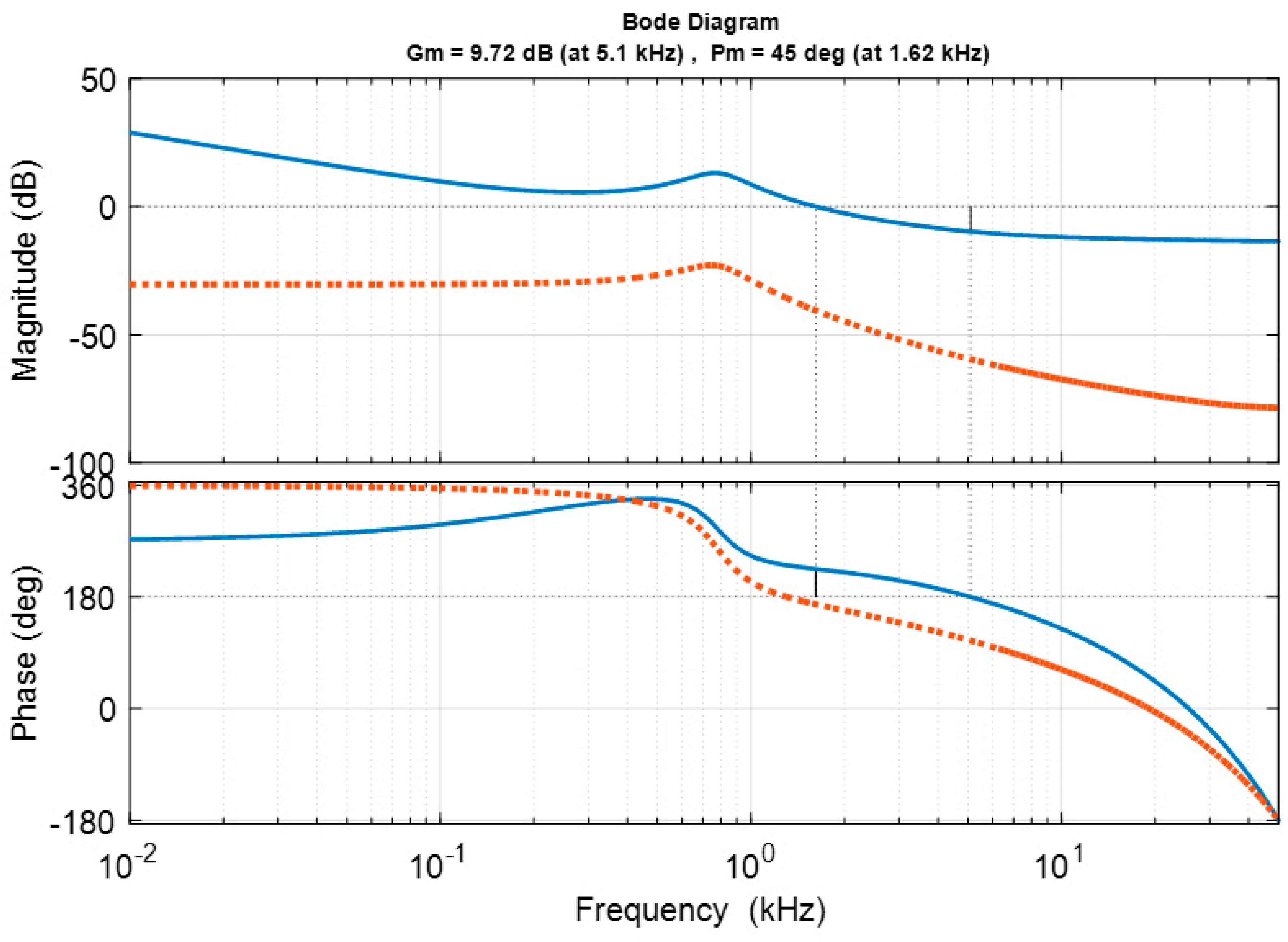
4.1. Experimental Results for Battery Module Voltage Control Loop

For the test of battery module voltage control loop, the reference output voltage for each battery module was changed suddenly from 10 V (VMX1-DC-ref = VMX2-DC-ref = VMX3-DC-ref = 10 V under steady-state operation) to VMX1-DC-ref = 13 V, VMX2-DC-ref = 9 V and VMX3-DC-ref = 8 V. The simulation results and experimental results are shown in Figure 9.
From Figure 9, it can be observed that once the reference voltage values were changed, the output voltage of battery module 1 was controlled to increase while the output voltages of battery modules 2 and 3 were controlled to decrease. In Figure 9, the simulation model results and the hardware experimental results are in good agreement. In other words, the shape, magnitude, and overshoot/undershoot of the waveforms of simulation and hardware experiments match each other, which validates the small-signal model for the battery module voltage loop.

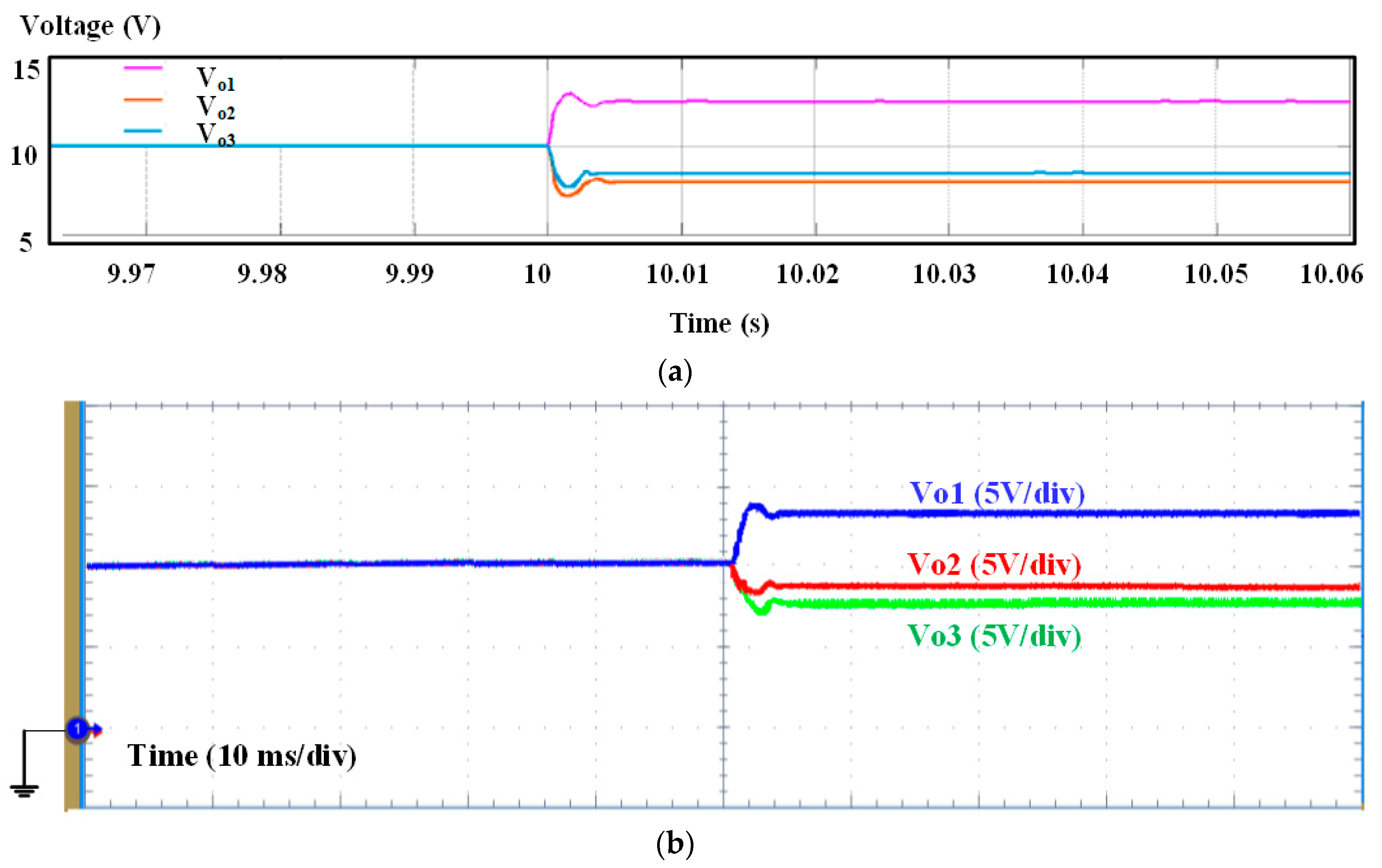
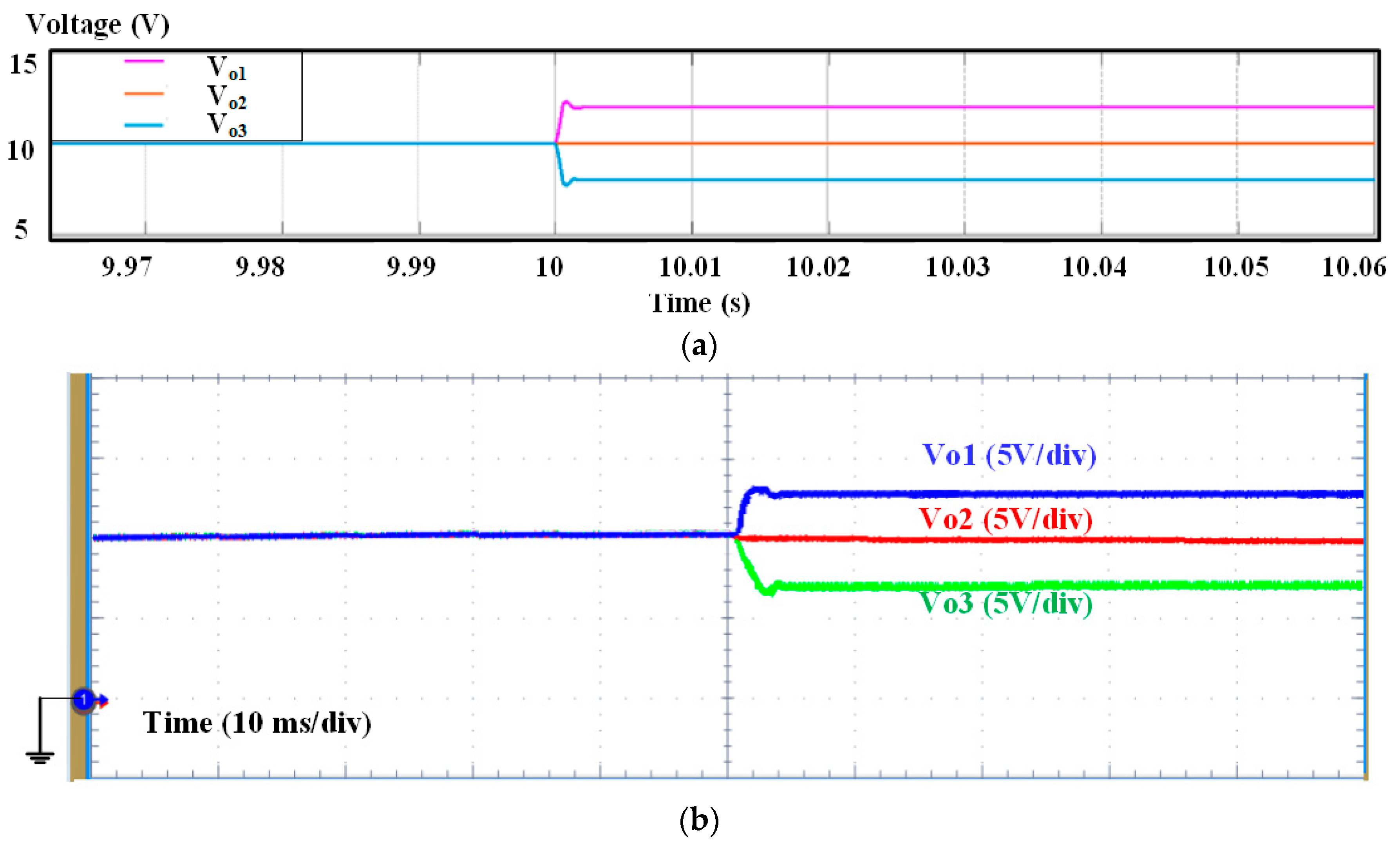
4.2. Experimental Results for SOC Balancing Control Loop

For the test of SOC balancing control loop, the SOC value of three battery modules were changed suddenly from SOC1 = SOC2 = SOC3 = 70% under balanced conditions to SOC1 = 75%, SOC2 = 70%, and SOC3 = 65%. The experimental results are shown in Figure 10.
It can be observed from Figure 10 that once there was a change in SOC values, Vo1 increased while Vo3 decreased. This is because the value of SOC1 was larger than the average SOC value of three battery modules (i.e., (75% + 70% + 65%)/3 = 70%), therefore resulted in a larger value of the battery module output voltage Vo1 for faster discharge. The variation of Vo3 for battery module 3 followed the same behavior but in the opposite direction. The value of SOC2 was equal to the average SOC value, and therefore, its corresponding battery module output voltage remained constant. Figure 10 also shows that the simulation results and hardware experimental results are in good agreement under the variation of SOC values test condition.

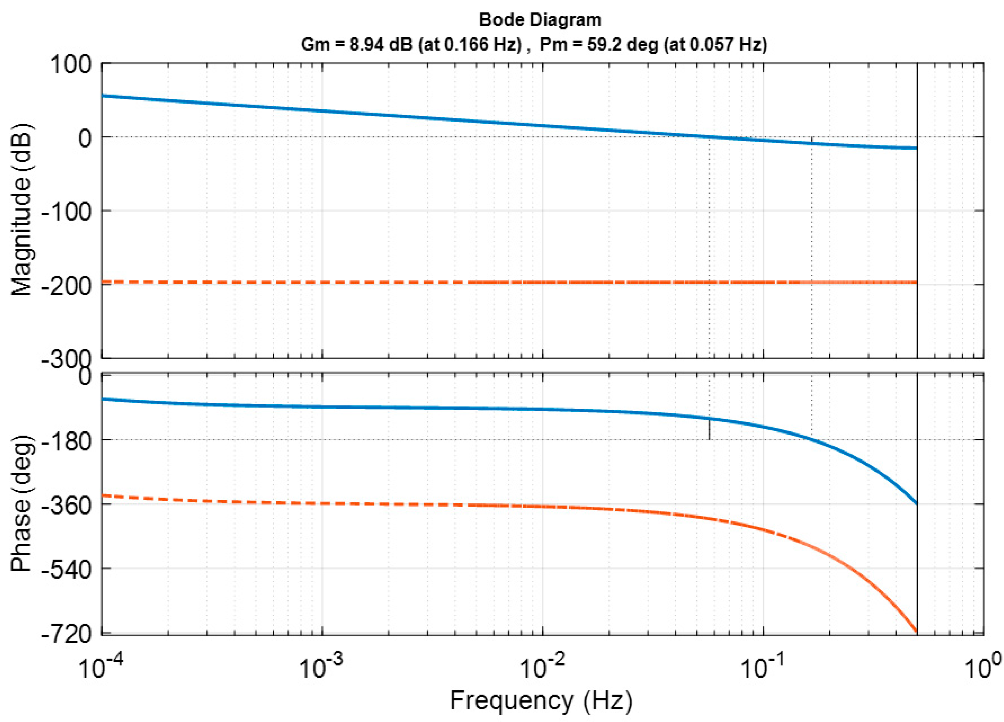
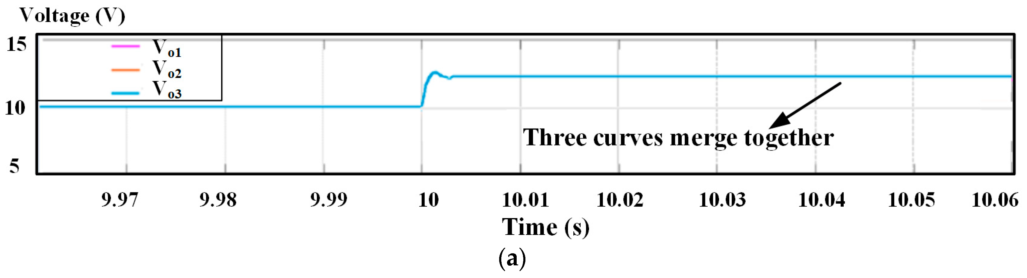
4.3. Experimental Results for Bus Voltage Control Loop

The last test was implemented for the bus voltage control loop. In this test, the bus voltage reference value was changed suddenly from 30 V to 37.5 V, as shown in Figure 11. It can be observed from Figure 11 that as the bus voltage reference value increased, the battery module voltage values changed from 10 V to 12.5 V correspondingly, which yielded a total bus voltage equal to its new reference value. The waveforms shown in Figure 11 demonstrate the consistency between simulation results and hardware experimental results.

5. Additional Comment

It should be noted that the presented WEDES system in this paper is different from a traditional Inductor-Capacitor (LC) compensation wireless power transfer (WPT) system or a traditional battery energy storage system (BESS). Instead, it is a combination of both systems. Table 2 shows a comparison between the presented WEDES system in this paper, conventional WPT system [18,21,22], and conventional BESS system [23,24,25]. It is shown that the presented WEDES system combines the advantages of both the conventional WPT system and BESS system, and can achieve bus voltage regulation and SOC balancing, and allow for fast and safe exchange/swapping of smaller and lighter battery modules with WPT technology.

6. Conclusions

In this paper, the small-signal modeling of a distributed WEDES battery system was derived to analyze the steady-state stability and dynamic response of the entire system, as well as provide guidelines for the controller design of multiple interacted control loops. Based on the small-signal models and associated transfer functions, all three control loops, including battery module output voltage control loop, SOC balancing control loop, and bus voltage control loop with compensators, were evaluated and validated by both simulations and a 3-module WEDES battery system. It was shown that the experimental results from simulation and hardware prototype were in good agreement, which validates the accuracy and effectiveness of the derived small-signal model and designed compensators.

Author Contributions

Y.C. and J.A.Q. both devised the concept of the model. J.A.Q. directed the simulation and experimental work based on his previous work and Y.C. performed simulations and experiments and obtained results. Y. C. drafted the manuscript and finalized it (responsible for the final version of the paper manuscript). J.A.Q. reviewed the manuscript draft and provided feedback. This work was done at The University of Alabama when Y.C. was the Ph.D. student of J.A.Q. and working in the research lab of J.A.Q.

Funding

This research received no external funding.

Conflicts of Interest

The author declares no conflict of interest.

References

  1. Abu Qahouq, J.; Cao, Y. Control scheme and power electronics architecture for a wirelessly distributed and enabled battery energy storage system. Energies 2018, 11, 1887. [Google Scholar] [CrossRef]
  2. Lelie, M.; Braun, T.; Knips, M.; Nordmann, H.; Ringbeck, F.; Zappen, H.; Sauer, D.U. Battery management system hardware concepts: An overview. Appl. Sci. 2018, 8, 534. [Google Scholar] [CrossRef]
  3. Charging Station (Battery Swapping section). Wikipedia, the Free Encyclopedia. Available online: https://en.wikipedia.org/wiki/Charging_station#Battery_swapping (accessed on 24 August 2019).
  4. Shao, S.; Guo, S.; Qiu, X. A mobile battery swapping service for electric vehicles based on a battery swapping van. Energies 2017, 10, 1667. [Google Scholar] [CrossRef]
  5. Hou, J.; Yang, Y.; He, H.; Gao, T. Adaptive Dual Extended Kalman Filter Based on Variational Bayesian Approximation for Joint Estimation of Lithium-Ion Battery State of Charge and Model Parameters. Appl. Sci. 2019, 9, 1726. [Google Scholar] [CrossRef]
  6. Cao, Y.; Abu Qahouq, J.A. Analysis and Evaluation of a Dual-Variable Closed-Loop Control of Power Converter with Wireless and Nonwireless Power Transfer. IEEE Trans. Ind. Electron. 2019, 66, 2668–2679. [Google Scholar] [CrossRef]
  7. Chen, J.; Chen, C.; Duan, S. Cooperative Optimization of Electric Vehicles and Renewable Energy Resources in a Regional Multi-Microgrid System. Appl. Sci. 2019, 9, 2267. [Google Scholar] [CrossRef]
  8. Rakhymbay, A.; Khamitov, A.; Bagheri, M.; Alimkhanuly, B.; Lu, M.; Phung, T. Precise analysis on mutual inductance variation in dynamic wireless charging of electric vehicle. Energies 2018, 11, 624. [Google Scholar] [CrossRef]
  9. Schroeder, A.; Traber, T. The economics of fast charging infrastructure for electric vehicles. Energy Policy 2012, 43, 136–144. [Google Scholar] [CrossRef]
  10. Kong, P.Y.; Karagiannidis, G. Charging schemes for plug-in hybrid electric vehicles in smart grid: A. survey. IEEE Access 2016, 4, 6846–6875. [Google Scholar] [CrossRef]
  11. Deutsches Elektronen-Synchrotron DESY. Fast Charging Cycles Make Batteries Age More Quickly: X-Ray Study Images Damage in Lithium-Ion Batteries. Science Daily. April 2015. Available online: www.sciencedaily.com/releases/2015/04/150414094117.htm (accessed on 24 August 2019).
  12. Chandrasekaran, R. Quantification of bottlenecks to fast charging of lithium-ion-insertion cells for electric vehicles. J. Power Sources 2014, 271, 622–632. [Google Scholar] [CrossRef]
  13. Whitney, L. Tesla Demos Electric Battery Swap in just 90 Seconds. CNET. June 2013. Available online: https://www.cnet.com/news/tesla-demos-electric-battery-swap-in-just-90-seconds/ (accessed on 24 August 2019).
  14. Miller, J.M.; Jones, P.T.; Li, J.M.; Onar, O.C. ORNL experience and challenges facing dynamic wireless power charging of EV’s. IEEE Circuits Syst. Mag. 2015, 15, 40–53. [Google Scholar] [CrossRef]
  15. Zhu, Q.; Wang, L.; Liao, C. Compensate capacitor optimization for kilowatt-level magnetically resonant wireless charging system. IEEE Trans. Ind. Electron. 2014, 61, 6758–6768. [Google Scholar] [CrossRef]
  16. Zhang, L.; Peng, H.; Ning, Z.; Mu, Z.; Sun, C. Comparative research on RC equivalent circuit models for lithium-ion batteries of electric vehicles. Appl. Sci. 2017, 7, 1002. [Google Scholar] [CrossRef]
  17. Luo, Z.; Wei, X. Analysis of square and circular planar spiral coils in wireless power transfer system for electric vehicles. IEEE Trans. Ind. Electron. 2018, 65, 331–341. [Google Scholar] [CrossRef]
  18. Cao, Y.; Abu Qahouq, J.A. Modelling and control design of reconfigurable wireless power transfer system for transmission efficiency maximization and output voltage regulation. IET Power Electron. 2019, 12, 1903–1916. [Google Scholar] [CrossRef]
  19. Dang, Z.; Cao, Y.; Abu Qahouq, J.A. Reconfigurable Magnetic Resonance-Coupled Wireless Power Transfer System. IEEE Trans. Power Electron. 2015, 30, 6057–6069. [Google Scholar] [CrossRef]
  20. Erickson, R.W.; Maksimovic, D. Fundamentals of Power Electronics; Springer: Berlin/Heidelberg, Germany, 2001; pp. 265–330. [Google Scholar]
  21. Wang, Y.; Lin, F.; Yang, Z.P.; Liu, Z.Y. Analysis of the Influence of Compensation Capacitance Errors of a Wireless Power Transfer System with SS Topology. Energies 2017, 10, 2177. [Google Scholar] [CrossRef]
  22. Galigekere, V.P.; Pries, J.; Onar, O.C.; Su, G.; Anwar, S.; Wiles, R.; Seiber, L.; Wilkins, J. Design implementation of an optimized 100 kW stationary wireless charging system for EV battery recharging. In Proceedings of the 2018 IEEE Energy Conversion Congress and Exposition (ECCE), Portland, OR, USA, 23–27 September 2018; pp. 3587–3592. [Google Scholar]
  23. Cao, Y.; Abu Qahouq, J.A. Evaluation of bi-directional single-inductor multi-input battery system with state-of-charge balancing control. IET Power Electron. 2018, 11, 2140–2150. [Google Scholar] [CrossRef]
  24. Efstratios, C.; Rogers, D.J. Cell SoC balancing using a cascaded full bridge multilevel converter in battery energy storage systems. IEEE Trans. Ind. Electron. 2016, 63, 5394–5402. [Google Scholar]
  25. Qian, H.; Zhang, J.; Lai, J.S.; Yu, W. A high-efficiency grid-tie battery energy storage system. IEEE Trans. Power Electron. 2011, 26, 886–896. [Google Scholar] [CrossRef]
Figure 1. Illustration diagrams of battery system for electric vehicle (EV) application. (a) The conventional battery pack and electrics drive system in EVs, (b) the wireless distributed and enabled battery energy storage (WEDES) battery system in EVs, and (c) example circuit diagram of the WEDES system [1].
Applsci 09 04249 g001aApplsci 09 04249 g001b
Figure 2. Illustration of the WEDES controller presented in [1].
Applsci 09 04249 g002
Figure 3. Small-signal of distributed the WEDES battery system with the WEDES controller.
Applsci 09 04249 g003
Figure 4. Circuit diagram of DC-DC boost stage in the WEDES system.
Applsci 09 04249 g004
Figure 5. Circuit diagram of the wireless power transfer (WPT) stage in the WEDES system (a) equivalent circuit and (b) T-model.
Applsci 09 04249 g005
Figure 6. The bode plot of the uncompensated (red-dashed curve) and compensated (blue-solid curve) battery module voltage control loop gain.
Applsci 09 04249 g006
Figure 7. The bode plot of uncompensated (red-dashed curve) and compensated (blue-solid curve) SOC balancing control loop.
Applsci 09 04249 g007
Figure 8. The bode plot of the uncompensated (red-dashed curve) and compensated (blue-solid curve) bus voltage control loop gain.
Applsci 09 04249 g008
Figure 9. Waveforms for three battery module output voltage when the reference voltages were changed from VMX1-DC-ref = VMX2-DC-ref = VMX3-DC-ref = 10 V to VMX1-DC-ref = 13 V, VMX2-DC-ref = 9 V and VMX3-DC-ref = 8 V, (a) simulation results and (b) hardware experimental results.
Applsci 09 04249 g009
Figure 10. Waveforms for three battery module output voltage when SOC values of three modules changed from SOC1 = SOC2 = SOC3 = 70% to SOC1 = 75%, SOC2 = 70%, and SOC3 = 65%, (a) simulation results and (b) hardware experimental results.
Applsci 09 04249 g010
Figure 11. Waveforms for three battery module output voltage when bus reference voltage changes from Vbus-ref = 30 V to Vbus-ref = 37.5 V, (a) simulation results and (b) hardware experimental results.
Applsci 09 04249 g011aApplsci 09 04249 g011b
Table 1. Design parameters of the wireless distributed and enabled battery energy storage (WEDES) system.
ParameterValueParameterValue
VMXr0–20 VLT, LR24 µH
Vbus-ref30 VCT, CR0.4 µF
Iout2 AkTR0.3
LMXr47 µHRpT, RRT @ 50 kHz0.1 Ω
CMXr220 µFfsw_bridge50 kHz
fsw_converter100 kHz--
Table 2. Comparison summary between the WEDES system, conventional Inductor-Capacitor (LC) compensation wireless power transfer (WPT) system, and conventional battery energy storage system (BESS).
ParameterWEDES System in this PaperConventional LC Compensation WPT System [18,21,22]Conventional BESS System [23,24,25]
Typical Components/DevicesBattery cells, power converter, inverter, WPT coils, and rectifierBattery cells, inverter, WPT coils, and rectifierBattery cells and power converter/inverter
System ComplexityMediumMediumLow
Able to Realize SOC BalancingYesNoYes
Able to Realize Voltage RegulationYesYesYes
Typical Battery OperationDischarging ChargingDischarging
Able to Transfer Power WirelesslyYesYesNo
Able to Insert/Remove Battery Module during Normal OperationYesNoNo
EfficiencyHigh (>85%)High (>90% at short distance)Highest (>95%)

