Article

Mass Transfer of Microscale Light-Emitting Diodes to Unusual Substrates by Spontaneously Formed Vertical Tethers During Chemical Lift-Off

1
Korea Photonics Technology Institute (KOPTI), Gwangju 500-460, Korea
2
Department of Photonic Engineering, Chosun University, Gwangju 501-759, Korea
3
Department of Mechanical Engineering, University of Houston, Houston, TX 77204-2004, USA
*
Author to whom correspondence should be addressed.
Appl. Sci. 2019, 9(20), 4243; https://doi.org/10.3390/app9204243
Submission received: 18 September 2019 / Revised: 2 October 2019 / Accepted: 6 October 2019 / Published: 11 October 2019
(This article belongs to the Special Issue GaN-Based Light-Emitting Diodes)

Abstract

:
A much simplified method for transferring Gallium nitride (GaN) light emitting didoes (LEDs) to an unusual substrate, such as glass, Si, polyethylene terephthalate, or polyurethane, was demonstrated with spontaneously formed vertical tethers during chemical lift-off (CLO), without requiring a sacrificial layer or extra process steps. The LED arrays resided on a stamp that was coated with an adhesive layer. After the layer with the LEDs was transferred to the new substrates, the stamp was removed by acetone to complete the preparation. Over 3 × 3 cm2 LED arrays transferred to various substrates without any damage and misorientation. We also found that the optical and electrical characteristics improved after transfer due to decease in built-in stress. This simple and practical method is expected to greatly facilitate the development of transferrable full color GaN microLEDs on various substrates with either greatly reduced or no damage.

Graphical Abstract

1. Introduction

Large-scale and flexible electronic and optoelectronic devices have recently attracted much attention for use in wearable displays, solar cells, sensors, and biomedical devices [1,2]. For flexible, bendable, and wearable devices, organic films have been widely employed because of their excellent scalability and flexibility. Compared to inorganic materials, however, organic films have drawbacks such as a short lifetime, low efficiency, low brightness, difficulty in enlarging, and low stability in humid environments. Gallium nitride (GaN)-based microscale light-emitting diodes (microLEDs) have attracted substantial attention in recent years as they have the potential to replace conventional organic light-emitting diodes (OLEDs) for flexible and bendable displays [3,4].
Conventional routes to these devices involve epitaxial growth of active materials followed by chip fabrication, wafer dicing, and pick-and-place robotic manipulation into individually packaged components for interconnection by bulk wire-bonding. However, dicing becomes more difficult as the chip size decreases beyond 100 μm × 100 μm, and integrating them on flexible and bendable substrates also becomes a challenge. Therefore, another route has been suggested for the manufacture of electronic devices, and it involves chip fabrication, the separation of chips from the mother substrate, and transfer of separated chips to devices. There are two ways to separate chips from a substrate, namely laser lift off (LLO) and chemical lift off (CLO) [5]. Generally, separating GaN LEDs from a sapphire substrate by LLO is an expensive process because it requires the use of a deep ultraviolet excimer laser [6,7,8]. In addition, the current LLO process requires a series of complicated steps to transfer-print the GaN LED structure onto a flexible substrate, including bonding the structure to a hard substrate before LLO, selective removal of the bonding layer after LLO, transferring the flexible substrate using an elastomeric stamp, another round of transfer-printing if a flip transfer is necessary, and a long process time [5,9]. The transfer of GaN films to receptor substrates results in a considerable release of stresses, which originate from the large lattice and thermal mismatch between the GaN-based layers and sapphire substrate. The released stresses may result in structural defects and even cracks in the epitaxial layers that degrade device performance [10]. Therefore, there is a strong need to develop a simplified method for higher-yield transfer while preserving the original layout of the GaN LEDs. Recently, Trindade et al. reported the scalable pick-and-place transfer-printing of GaN LEDs fabricated on silicon onto a mechanically flexible substrate through CLO, using a horizontal tether as the sacrificial layer and anchor to hold the isolated LED chips [11]. For thin-film LEDs, the device-processing steps for GaN LEDs fabricated on a Si substrate are almost identical to those for GaN LEDs on a sapphire substrate, except that the former requires the host substrate to be removed in a simple chemical mechanical process, while the latter uses an LLO process. Therefore, this method has the advantage of a short process time, simple steps, and low damage of the epilayer without using a high-power UV laser during the LLO process. In addition, with the significant improvements in growth and fabrication techniques, the current external quantum efficiency of GaN LEDs on a silicon substrate represents an improvement of 65% and is comparable to that of GaN LEDs on sapphire [12]. GaN LEDs can be grown on large-scale Si wafers, e.g., Si(111) substrates with diameters of up to 200 mm, which are cheaper than sapphire wafers. The GaN-on-silicon approach also benefits from the use of existing equipment for silicon manufacturing [13]. However, the pick-and-place transfer-printing method requires expensive equipment, a long process time, and a sacrificial layer. In addition, the characteristics related to wavelength shift and efficiency before and after transfer of the LEDs are not well known.
Here, we suggest a simplified transfer-printing method for GaN LEDs grown on a silicon wafer through spontaneously formed vertical tethers during the CLO process. This method does not require an additional sacrificial layer or extra process steps such as the fabrication of an anchor that would allow the development of mass transfer for flexible devices. The optical characteristics of the GaN LEDs, before and after transfer, were studied by Raman, microphotoluminescence (microPL), and electroluminescence (EL) spectroscopy.

2. Experimental

Figure 1a shows a schematic diagram of GaN-based LEDs on a Si substrate. The GaN-based LED structure (operating at a dominant emission peak of 450 nm) was grown on an Si(111) substrate using metal-organic chemical vapor deposition. The LEDs consisted of the following layers: a Si-doped n-GaN layer that was 2 µm thick, a molecular quantum well (MQW) active layer consisting of five periods of un-doped InGaN wells and un-doped GaN barriers, and a Mg-doped p-GaN layer with thickness of 0.15 µm a hole concentration of 3 × 1017 cm−3. In order to fabricate the LEDs, which were 100 × 100 µm2 in size, the p-GaN layer was etched using an inductively coupled plasma (ICP) that utilized Cl2 and BCl3 source gases until the n-GaN layer was exposed for n-type contact. After mesa etching, the GaN LEDs were isolated to separate them from the Si substrate by using an ICP that utilized Cl2 and BCl3 source gases until the surface of the Si substrate was exposed. The LEDs were then fabricated using an indium–tin oxide (ITO) layer that was 200 nm thick as a transparent current-spreading layer. A Cr (30 nm) and a Au (100 nm) layer were deposited by e-beam evaporation as the n- and p-pad electrodes, respectively.
To prepare the devices for their later release from the native substrate, they were underetched by anisotropic wet etching with a 60 wt% aqueous potassium hydroxide (KOH) solution at 80 °C. The etch rate in the (110) direction was faster than that in the (111) direction. As a result, the Si(110) plane was preferentially etched in the lateral direction. Upon completion of the underetching, the LEDs were suspended above the Si substrate, resting on small hexagonal pillars that could spontaneously serve as vertical tethers, as shown in Figure 1. Next, the isolated microLED arrays were coated with poly(methyl methacrylate) (PMMA), and the remaining pillars were removed by wet etching with KOH, as shown Figure 1b–d. The LED arrays with the PMMA stamp were moved to unusual substrates such as Si, glass, polyethylene terephthalate (PET), or stretchable polyurethane (PU). Finally, the PMMA was removed by acetone, as shown in Figure 1e.

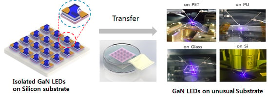
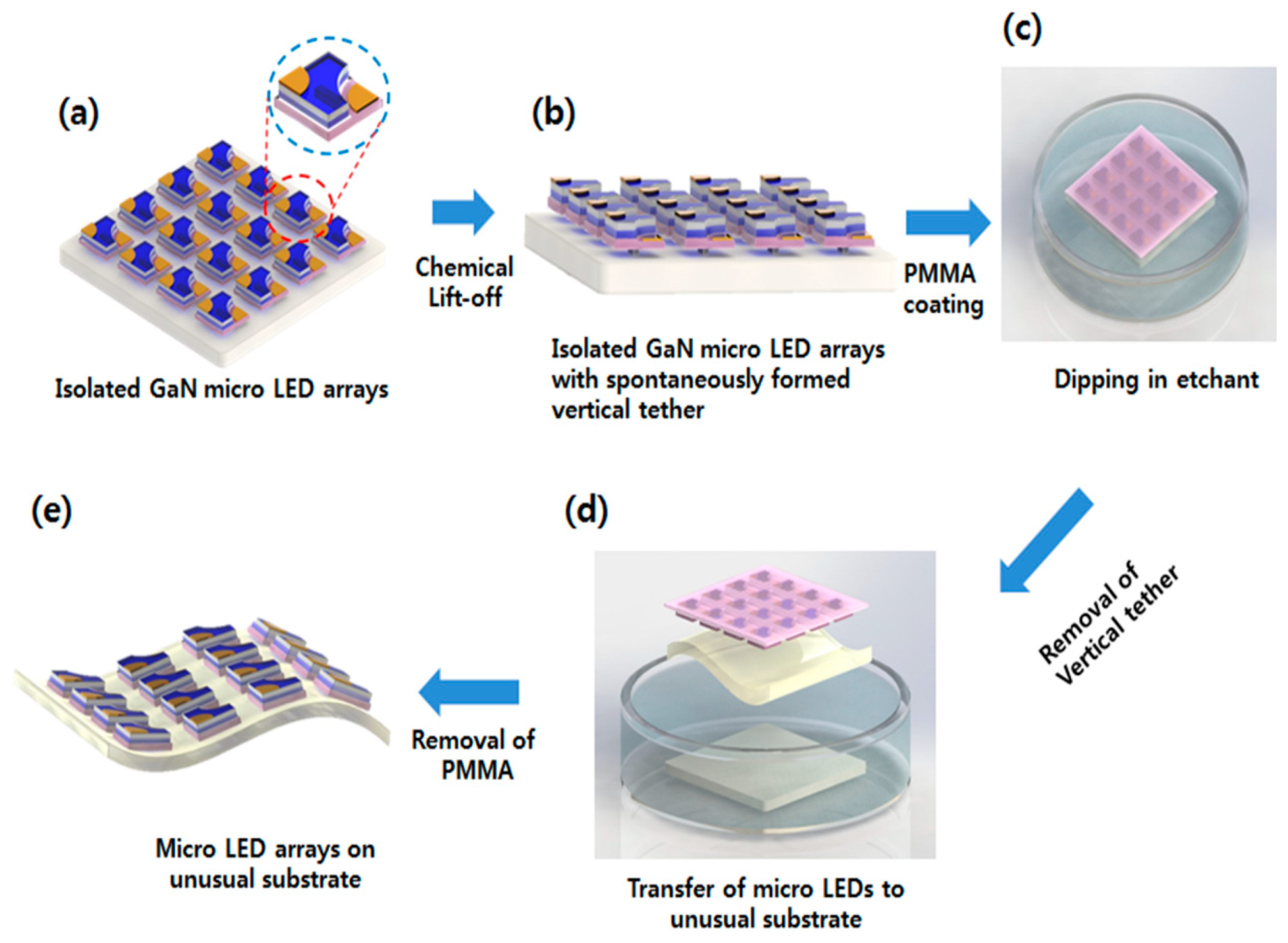
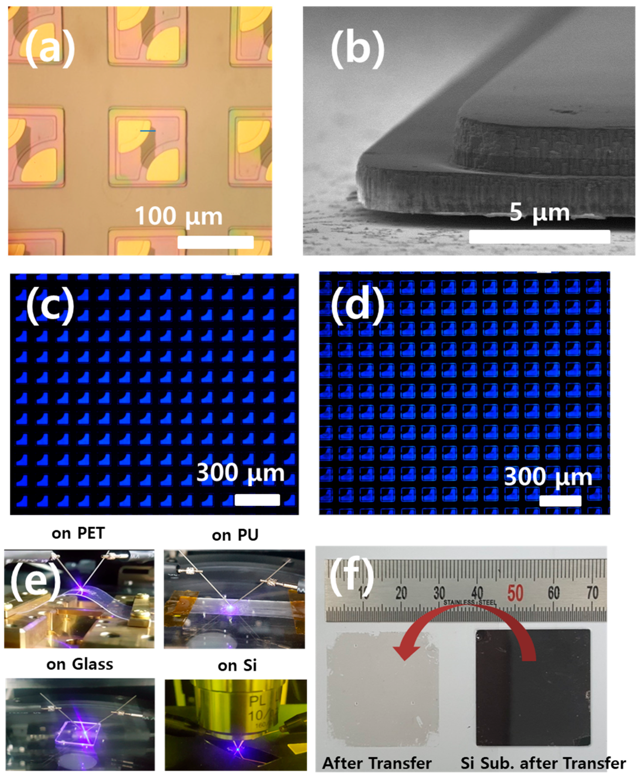
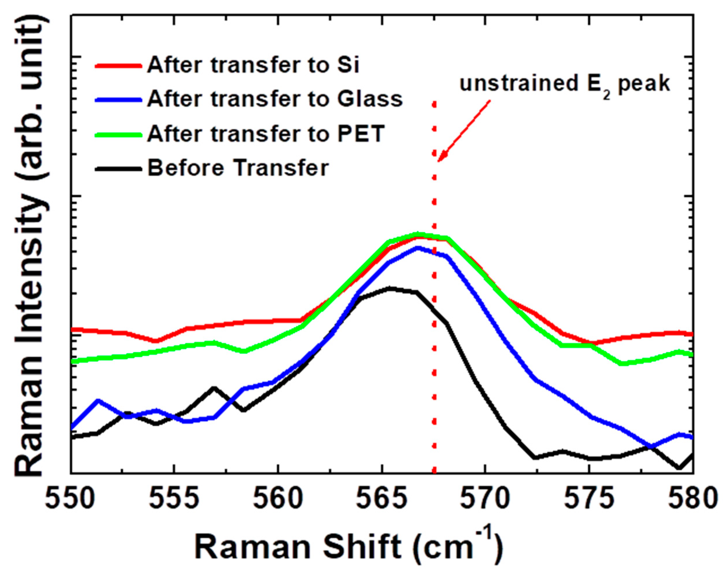
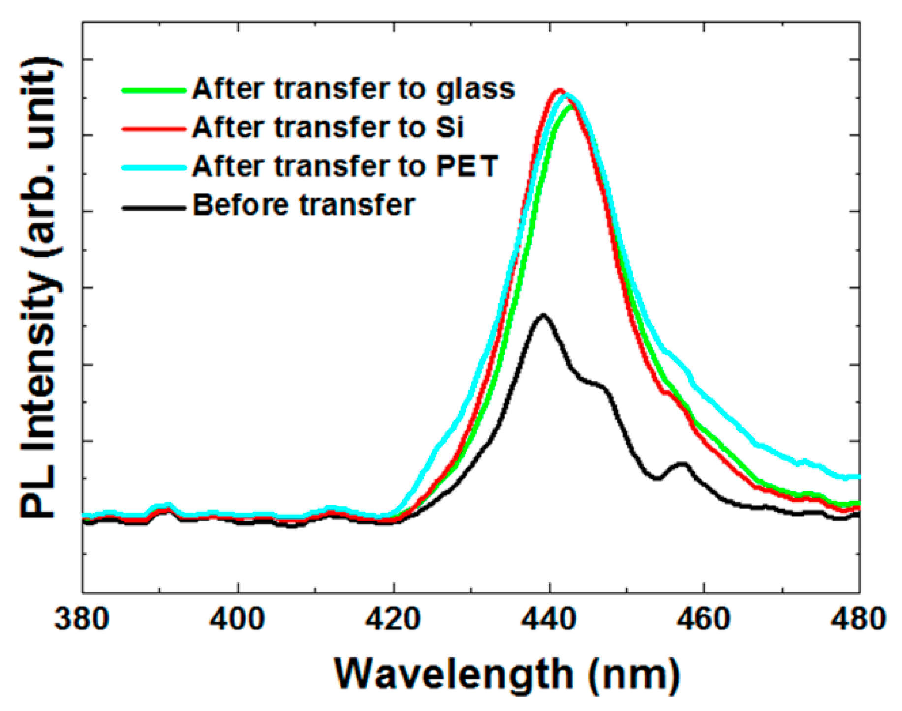
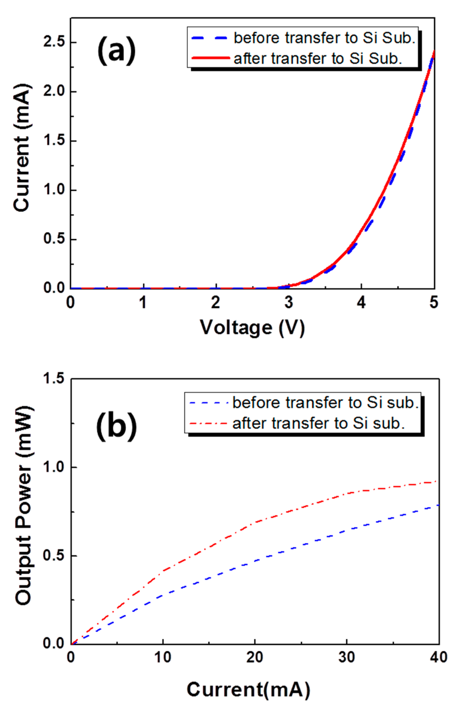
3. Results and Discussion

Figure 2 shows optical microscope images and field-emission scanning electron microscope (FE-SEM) images before and after the CLO process. To detach the LED arrays from the Si substrate, we used spontaneously formed vertical tethers during the CLO process. Supplementary Figure S1 shows that Si was etched anisotropically with increasing etching time, where the Si(110) plane is defined as the lateral direction. Figure 2a,b shows that the cross-sectional area of the spontaneously formed vertical Si tethers was 52 × 21 µm2 and the height was 710 nm before the deposition of PMMA. These vertical Si tethers were removed by additional etching with KOH. The PMMA stamp holding the microLED arrays was moved to the glass substrate, and the PMMA was removed by acetone to expose the microLED arrays. Figure 2c,d shows the PL mapping images of GaN LED before and after transfer to glass substrate. It clearly shows that there was no degradation of optical properties and a shift in spacing between the LEDs. These results demonstrate that, unlike LLO, CLO is a damage-free process. Figure 2e shows the emission images of GaN LEDs on various transparent, flexible, or rigid substrates. Figure 2f shows an area measuring 3 × 3 cm2 that was transferred to a glass substrate. These results show that the CLO approach is not dependent on the size of the transfer area.
Figure 3 shows Raman spectra of the three samples measured at room temperature. In the spectrum of the GaN LEDs before transfer, the peak at 565.4 cm−1 corresponds to the E2 mode of the GaN hexagonal phase. It has been previously shown that the E2 mode Raman peak of unstrained hexagonal GaN is located at 567.4 cm−1 [14]. The relationship between the E2 mode Raman peak shift (Δωy) and the in-plane biaxial stress (σχχ) can be expressed as [14,15]:
σχχ = Δωy/Ky
where σχχ is the stress in GPa, Δωy is the Raman peak shift in cm−1, and Ky is the stress coefficient (4.3 cm−1 GPa−1). The stress on the GaN surface before transfer was estimated to be 0.465 GPa, which means that the GaN epilayer on the Si substrate had high tensile stress. The E2 Raman peak in the spectra obtained for the GaN LEDs on Si, glass, and PET substrates after transfer is shifted to 567.1 cm−1. The stress on the GaN surface was estimated to be 0.07 GPa after transfer, indicating that the tensile strain was fully released. Since tensile stress can blue shift an emission peak and reduce the efficiency of a device, a red-shift of the emission peak and improvement in the LED efficiency are expected in the spectrum obtained after transfer.
The strain of the MQW layer is more effectively released after transfer to Si, which is proven by X-ray reciprocal space mapping (RSM) of the (105) reflector for sample before and after transfer to Si (Supplementary Figure S2). The vertical solid line represents the fully strained axis. As shown in Supplementary Figure S2a,b, a larger horizontal shift of the InGaN peak with respect to the GaN peak is observed for the sample after transfer to Si, indicating a higher strain relaxation in the MQW layer. This result is identical to strain relaxation in the Raman spectra after transfer.
The strain of the MQW layer is more effectively released after transfer to Si, which is proven by X-ray reciprocal space mapping (RSM) of the (105) reflector for the sample before and after transfer to Si (Supplementary Figure S2). The vertical solid line represents the fully strained axis. As shown in Supplementary Figure S2a,b, a larger horizontal shift of the InGaN peak with respect to the GaN peak is observed for the sample after transfer to Si, indicating a higher strain relaxation in the MQW layer. This result is identical to the strain relaxation in Raman spectra after transfer.
Figure 4 shows the PL spectra, measured at room temperature, of the InGaN/GaN MQW LED structures before and after transfer onto various substrates. In the spectrum obtained before transfer, the LED emission peak at about 441 nm typically corresponds to the MQWs. However, in the spectrum obtained after transfer, the PL peak of GaN LEDs on Si, glass, and PET substrates is red-shifted to 442.4, 443.5, and 443.2 nm, respectively, because the tensile stress in the top GaN was reduced by the transfer via stress redistribution, as shown in Figure 3. The compressive strain of the InGaN QW material was also reduced in this regard. Two main effects could play important roles in the PL emission wavelength of the MQWs: One was the quantum-confined Stark effect (QCSE), which is related to the piezoelectric field, and the other was the bandgap shrinkage of InGaN within the MQWs. The first effect caused a blue shift while the latter caused a red shift in the PL emission when the compressive strain was reduced in the MQWs; their compensations led to the small red shift observed in the PL emissions. The small red shift of wavelength of LEDs on the glass and PET substrates resulted from an increase in joule heating when compared to the LEDs on the Si substrate. However, the reduced QCES would increase the spatial overlaps between the wave functions of electrons and holes within the QWs which could, in turn, significantly enhance the electron-hole recombination efficiency of the InGaN/GaN MQWs LEDs [16].
Figure 5a,b display the current–voltage (I–V) curves of GaN LEDs before and after transfer onto various substrates. To confirm that the reflection at the interface between the GaN LED and substrate was negligible, we compared the LEDs before and after transfer onto the Si substrate. Figure 5a shows that the electrical properties of the LEDs are not changed after transfer. This result shows that CLO is a damage-free process without degradation in the contact metal or formation of structural defects and cracks. Figure 5b displays the light output power of the InGaN/GaN LEDs before and after transfer. The light output intensity (at an injection current of 20 mA) of the LED after transfer was 33% higher than the output intensity of the LED before transfer. This improvement can be attributed to the enhancement of the electron-hole recombination efficiency with the decrease in QCSE by strain relaxation.

4. Summary

In this work, we demonstrated a simple transfer method with spontaneously formed vertical Si tethers during the CLO process for GaN LEDs onto flexible substrates. This method allows for the mass transfer of GaN LEDs and reduces the process time. After transfer, the tensile stress was significantly decreased, resulting in a red shift of the emission peak and improvement of the efficiency of GaN LEDs. The results reported here suggest that state-of-the-art GaN LEDs on Si substrates can be manipulated in the form of microLEDs in applications that would be difficult with conventional LED technologies.

Supplementary Materials

The following are available online at https://www.mdpi.com/2076-3417/9/20/4243/s1, Figure S1: Spontaneous formation of vertical tethers. Figure S2: RSM of X-ray diffraction intensity around the (105) reflector for micro LED (a) before and (b) after transfer to Si substrate.

Author Contributions

J.-Y.K., Y.-H.C., H.-S.P. and M.-K.K. conceived and designed the experiments; Y.-H.C. and H.-S.P. performed the experiments, J.-Y.K., J.-H.R. and M.-K.K. analyzed data and M.-K.K. wrote the paper.

Funding

This work was supported by a National Research Foundation (NRF) grant funded by the Republic of Korea (NRF-2016R1D1A1B01013847) and by “Human Resources Program in Energy Technology” of the Korea Institute of Energy Technology Evaluation and Planning (KETEP), granted financial resource from the Ministry of Trade, Industry and Energy, Republic of Korea (No. 20194030202410).

Conflicts of Interest

The authors declare no conflict of interest. The funders had no role in the design of the study; in the collection, analyses, or interpretation of data; in the writing of the manuscript, and in the decision to publish the results.

References

  1. Deol, R.S.; Choi, H.W.; Singh, M.; Jabbour, G.E. Printable displays and light sources for sensor applications: A review. IEEE Sens. J. 2015, 15, 3186. [Google Scholar] [CrossRef]
  2. Jeong, C.K.; Park, K.I.; Son, J.H.; Hwang, G.T.; Lee, S.H.; Park, D.Y.; Lee, H.E.; Lee, H.K.; Byun, M.; Lee, K.J. Self-powered fully-flexible light-emitting system enabled by flexible energy harvester. Energy. Environ. Sci. 2014, 7, 4035. [Google Scholar] [CrossRef]
  3. Huang, Y.; Tan, G.; Gou, F.; Li, M.; Lee, S.; Wu, S. Prospects and challenges of mini-LED and micro-LED displays. J. Soc. Inf. Disp. 2019, 27, 387. [Google Scholar] [CrossRef]
  4. Gou, F.; Hsiang, E.; Tan, G.; Chou, P.; Li, Y.; Lan, Y.; Wu, S. Angular color shift of micro-LED displays. Opt. Express 2019, 27, A746. [Google Scholar] [CrossRef] [PubMed]
  5. Wong, W.S.; Sands, T.; Cheung, N.W.; Kneissl, M.; Bour, D.P.; Mei, P.; Romano, L.T.; Johnson, N.M. Fabrication of thin-film InGaN light-emitting diode membranes by laser lift-off. Appl. Phys. Lett. 1999, 75, 1360. [Google Scholar] [CrossRef]
  6. Kim, T.I.; Jung, Y.H.; Song, J.Z.; Kim, D.; Li, Y.H.; Kim, H.S.; Song, I.S.; Wierer, J.J.; Pao, H.A.; Huang, Y.G.; et al. High-efficiency, microscale GaN light-emitting diodes and their thermal properties on unusual substrates. Small 2012, 8, 1643. [Google Scholar] [CrossRef] [PubMed]
  7. Seo, J.H.; Li, J.; Lee, J.; Gong, S.Q.; Lin, J.Y.; Jiang, H.X.; Ma, Z.Q. A simplified method of making flexible blue LEDs on a plastic substrate. IEEE Photonics J. 2015, 7, 8200207. [Google Scholar] [CrossRef]
  8. Choi, W.S.; Park, H.J.; Park, S.H.; Jeong, T. Flexible InGaN LEDs on a polyimide substrate fabricated using a simple direct-transfer method. IEEE Photonics. Technol. Lett. 2014, 26, 2115. [Google Scholar] [CrossRef]
  9. Zhang, J.Y.; Liu, W.J.; Chen, M.; Hu, X.L.; Lv, X.Q.; Ying, L.Y.; Zhang, B.P. Performance enhancement of GaN-based light emitting diodes by transfer from sapphire to silicon substrate using double-transfer technique. Nanoscale Res. Lett. 2012, 7, 244. [Google Scholar] [CrossRef] [PubMed]
  10. Hsu, S.C.; Pong, B.J.; Li, W.H.; Beechem, E.T.; Graham, S.; Liu, C.Y. Stress relaxation in GaN by transfer bonding on Si substrates. Appl. Phys. Lett. 2007, 91, 251114. [Google Scholar] [CrossRef] [Green Version]
  11. Trindade, A.J.; Guilhabert, B.; Massoubre, D.; Zhu, D.; Laurand, N.; Gu, E.; Watson, I.M.; Humphreys, C.J.; Dawson, M.D. Nanoscale-accuracy transfer printing of ultra-thin AlInGaN light-emitting diodes onto mechanically flexible substrates. Appl. Phys. Lett. 2013, 103, 253302. [Google Scholar] [CrossRef] [Green Version]
  12. Hahn, B.; Galler, B.; Engl, K. Development of high-efficiency and high-power vertical light emitting diodes. Jpn. J. Appl. Phys. 2014, 53, 100208. [Google Scholar] [CrossRef] [Green Version]
  13. Liu, H.F.; Seng, H.L.; Teng, J.H.; Chua, S.J.; Chi, D.Z. Effects of lift-off and strain relaxation on optical properties of InGaN/GaN blue LED grown on 150 mm diameter Si (111) substrate. J. Cryst. Growth 2014, 402, 155. [Google Scholar] [CrossRef]
  14. Tripathy, S.; Chua, S.J.; Chen, P.; Miao, Z.L. Micro-Raman investigation of strain in GaN and AlxGa1−xN/GaN heterostructures grown on Si(111). J. Appl. Phys. 2002, 92, 3503–3510. [Google Scholar] [CrossRef]
  15. Hsu, C.W.; Chen, Y.F.; Su, Y.K. Quality improvement of GaN on Si substrate for ultraviolet photodetector application. IEEE J. Quantum Electron. 2014, 50, 35. [Google Scholar] [CrossRef]
  16. Zhao, H.P.; Liu, G.Y.; Zhang, J.; Poplawsky, J.D.; Dierolf, V.; Tansu, N. Approaches for high internal quantum efficiency green InGaN light-emitting diodes with large overlap quantum wells. Opt. Express 2011, 19, A991–A1007. [Google Scholar] [CrossRef] [PubMed] [Green Version]
Figure 1. Schematic illustrations and images corresponding to steps for the transfer of Gallium nitride (GaN) light emitting diodes (LEDs): (a) isolated microLED arrays, (b) Isolated GaN micro LED arrays with spontaneously formed vertical tether, (c) deposition of PMMA and removal of remaining pillars, and (d) transfer of microLED arrays to unusual substrate. (e) MicroLED arrays on an unusual substrate.
Applsci 09 04243 g001
Figure 2. (a) Optical microscope image of GaN LED array with vertical tethers. (b) FE-SEM image of a GaN LED with a spontaneously formed vertical tether. PL mapping image of GaN LED (c) before transfer and (d) after transfer (e) Images of light emission from GaN LEDs transferred onto various substrates. FE-SEM image of GaN LEDs on a silicon substrate after transfer. (f) Optical microscope image of a GaN LED array (3 × 3 cm2) on a glass substrate after transfer.
Applsci 09 04243 g002
Figure 3. Raman spectra of GaN LEDs before and after transfer onto various substrates.
Applsci 09 04243 g003
Figure 4. PL spectra of GaN LEDs before and after transfer onto various substrates.
Applsci 09 04243 g004
Figure 5. (a) I–V curves and (b) optical output power of GaN LEDs before and after transfer onto the Si substrate.
Applsci 09 04243 g005

