Article

Effect of Fiber Weave Structure in Printed Circuit Boards on Signal Transmission Characteristics

1
School of Electronics Information Engineering, South China University of Technology, Guangzhou 510640, China
2
China Fastprint Circuit Corporation, Guangzhou 510663, China
3
Dongguan ITEQ Corporation, Dongguan 523000, China
*
Author to whom correspondence should be addressed.
Appl. Sci. 2019, 9(2), 353; https://doi.org/10.3390/app9020353
Submission received: 26 November 2018 / Revised: 28 December 2018 / Accepted: 11 January 2019 / Published: 21 January 2019
(This article belongs to the Special Issue Applied Sciences Based on and Related to Computer and Control)

Abstract

:
In this paper, we characterized and compared signal transmission performances of traces with different specifications of fiber weave. Measurements demonstrated that the dielectric constant, impedance fluctuation, and differential skew were all affected by fiber weave style. For flattened fiber weaves, the dielectric constant fluctuation reached 0.18, the impedance fluctuation amplitude was 1.0 Ω, and the differential skew was 2 ps/in. For conventional fiber weaves, the three parameters were 0.44, 2.5 Ω, and 4 ps/inch respectively. Flattened fiber weave was more favorable for high-speed signal control. We also discussed the other methods to improve the fiber weave effect. It turned out that NE-glass (new electronic glass) fiber weave also had better performance in reducing impedance fluctuation and differential skew. Furthermore, made the signal traces and fiber weave bundles with an angle or designing the long signal line parallel to the weft direction both are simple and effective methods to solve this problem.

1. Introduction

It is known that in today’s printed circuit board laminates, there is a plate-like material made of electronic glass fiber cloth that is impregnated with epoxy resin, covered with copper foil of a certain thickness on one or both sides, and then hot-pressed. The fiber weave and resin have relatively dielectric constant (Dk) of ~6 and ~3, respectively, presenting a nonhomogeneous medium for signal transmission. The performance of differential transmission traces is dependent upon the underlying material properties of the laminates used [1,2,3,4,5,6,7]. At high edge rates, especially transmission rates exceeding 25 Gbps, the impact of the fiber weave effect on high-speed signal transmission becomes non-negligible. For 25 Gbps single channel transmission rate or coming 56 Gbps, the fiber weave effect continues to challenge the PCB (short for Printed circuit board) industry to provide novel solutions. Research on the impact of fiber weave effect on ≥25 Gbps high-speed materials has become more meaningful. In this work, the dielectric constant fluctuations of different types of fiber weaves are studied using a vector network analyzer. Then the impact of the dielectric constant fluctuation on the impedance of single-ended lines and the signal propagation delay of differential lines are discussed. Furthermore, we also discuss the effect of trace direction on impedance fluctuation. Finally, we investigate different methods to improve the fiber weave effect. This paper allows high-speed digital designers to have a more in-depth assessment of the fiber weave effect.

2. Materials and Methods

2.1. Materials and Equipment
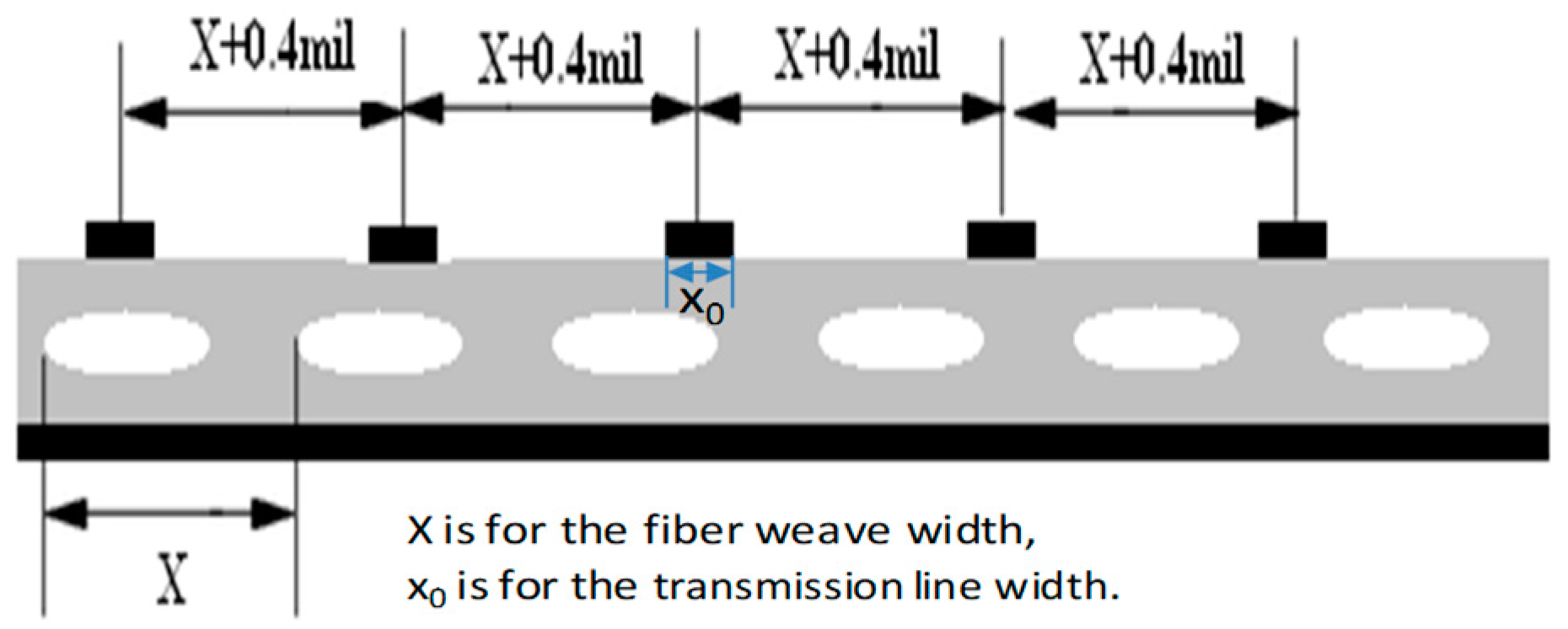
We focused on the fiber weave effect only for high-speed PCBs, so the research must be based on high-speed PCBs. Here, high-speed laminates and prepreg based on PPO (short for Polyphenylene Oxide) resins that were supplied by Panasonic were used to produce multilayer PCB.
A vector network analyzer (VNA, E5071C) from Agilent was used to measure TDR (short for time domain reflectometry), the S-parameter, and phase difference. To ensure the accuracy of the measurements, the tested frequency bandwidth was 20 GHz, and the rise time was 22.3 ps.

2.2. Methods

In the design of the tested multilayer board, the thicknesses of the laminate cores were 0.08 mm to 0.20 mm, and different styles of prepreg were used. The style of the fiber weaves contained prepreg 1035, prepreg 1080, prepreg 3313, prepreg 2116, and prepreg 1078.
The graphic design for the Dk test show as Figure 1: X was the width of the fiber weave bundle, and x0 was the transmission line width on the circuit board. Most transmission line were designed <10 mil, significantly less than most of the sizes of the fiber weaves (see Table 1, X2 and Y2). This would cause the transmission lines directly above the warp or weft fiber weave or in the middle of two fiber weaves (see Figure 1). Dk vary with the location of the transmission line. From Table 1, we can see that most spaces of the fiber weaves (the value of (X3 – X2) or (Y3 – Y2) in Table 1) <10 mil (0.4 mm), so we could design the spaces of single-ended microstrip lines to X + 0.4 mil to obtain the single-ended impedance across different positions of the fiber weaves.
We also designed differential microstrip lines (the other type of impedance line, other than a single-ended line) with different spaces to discuss impedance fluctuations influenced by the fiber weave effect.
The tested boards were produced by the following procedure: CCL (short for copper-clad laminate) cutting → inner layer process → laminating → drilling → PTH (short for plating through hole) → electronic plating → back drilling → outer layer process → solder mask → component mark → surface finishing → test.

3. Results and Discussion

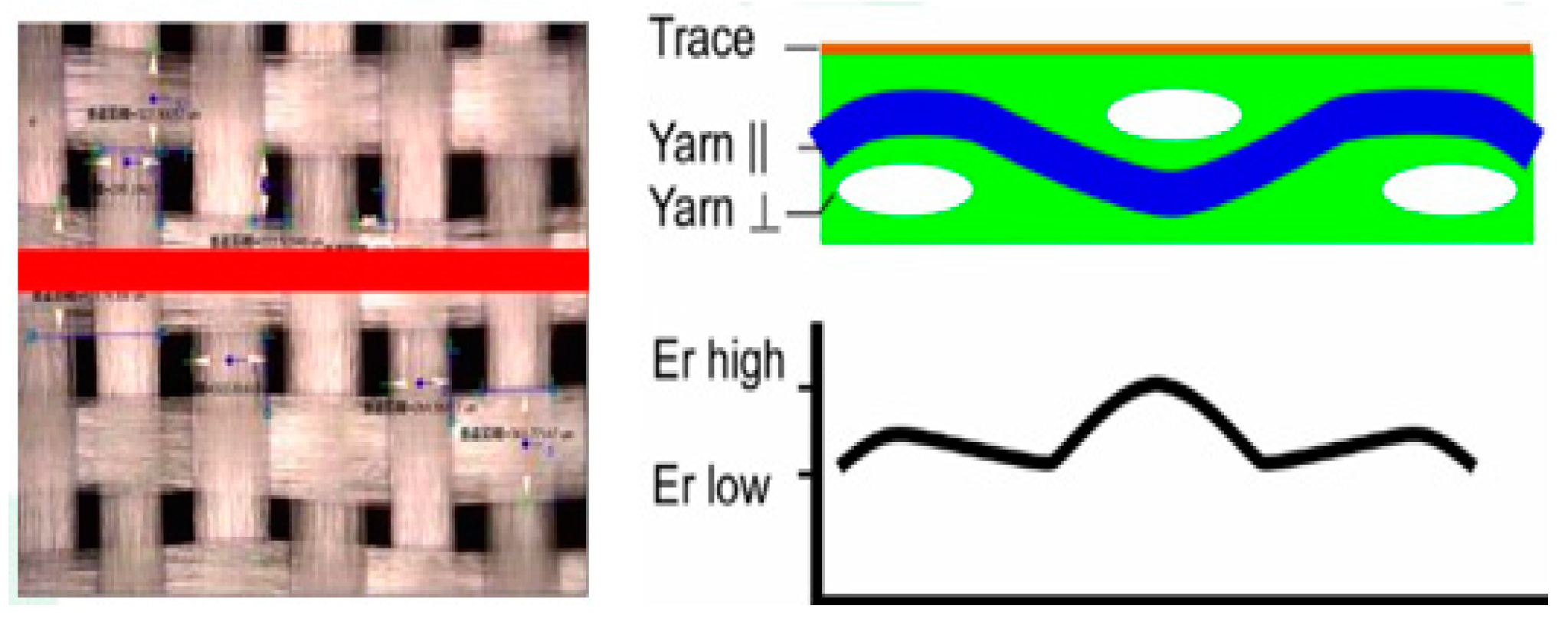
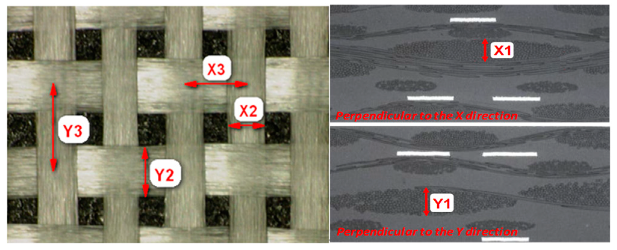
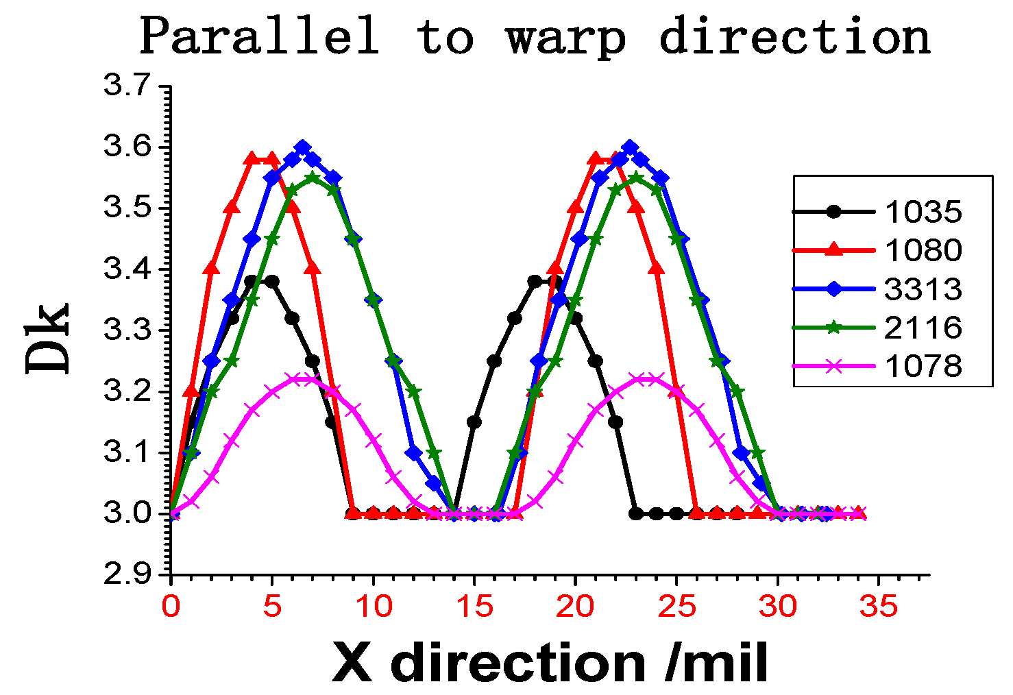
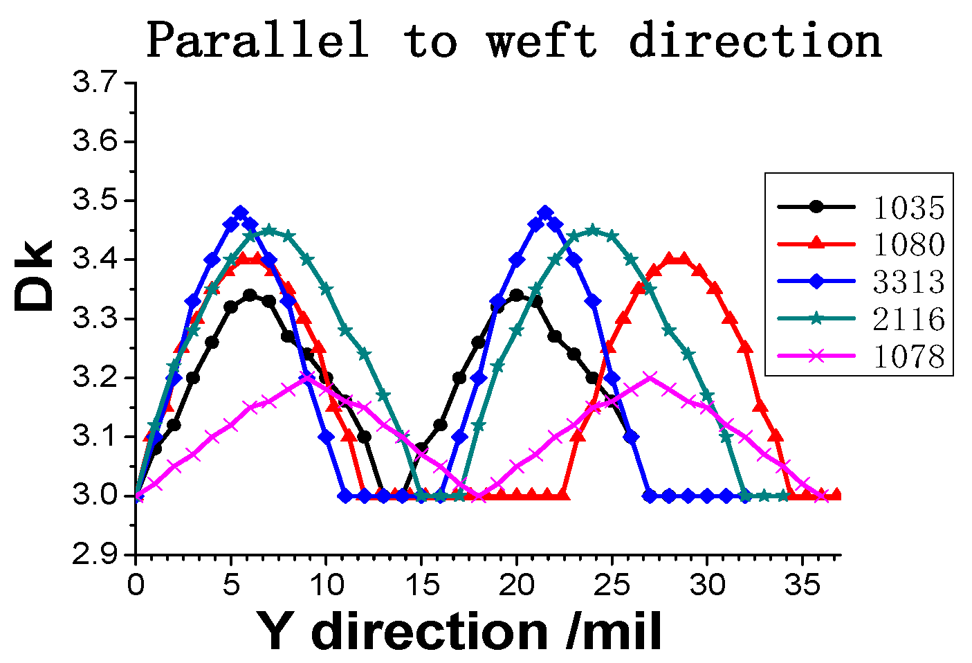
3.1. Dielectric Constant Fluctuations of Different Types of Fiber Weaves

Impedance fluctuations can be attributed to local variations in the Dk and the structural integrity of the stack-up, both of which depend on the laminate fiber weave. The dielectric constant (Dk) is a key parameter of impedance, and its fluctuation significantly affects impedance. Different types of fiber weaves show different characteristics.
For any particular stack-up configuration, there are two worst-case effective Dk extremes that occur, the highest and the lowest Dk. When all yarn strands align with each other, and the trace lies directly over the center of a low resin, a “glass peak” resin, the highest Dk is gotten. When the trace lies directly over the middle of a high resin, a “glass valley” region, the lowest Dk is gotten. Due to the trace passing across fiber weave bundles, like the feeling of crossing railroad tracks diagonally in a car (see Figure 2) [2], the trace exhibits a cyclical variation in Dk. For different styles of fiber weaves, fiber weave bundle dimensions are different, including a fiber weave bundle’s width (X2 and Y2) and pitch size (X3 and Y3) (see Figure 3 and Table 1). X represents warp direction, and Y represents weft direction.
With the parameters of X and Y, we could design different graphs to test Dk fluctuation amplitude for different styles of fiber weave. The fluctuation amplitude of Dk is shown in Figure 4 and Figure 5. It was found that the Dk fluctuation amplitudes of 1080, 3313, and 2116 were much larger than those of 1035 and 1078. Comparing warp direction to weft direction, it was found that the Dk fluctuation amplitude of weft direction was relatively lower than that of warp direction.

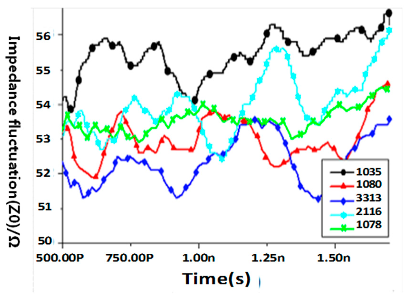
3.2. Impact of the Fiber Weave Effect on Impedance Fluctuations

There are two main types of transmission lines, differential lines and single-ended lines. The influence mechanism of the fiber weave effect on different impedance types is different.

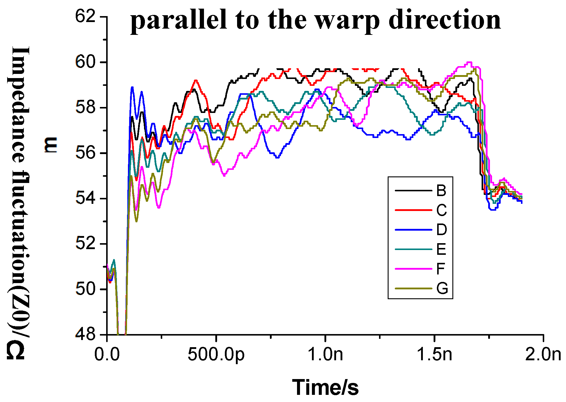
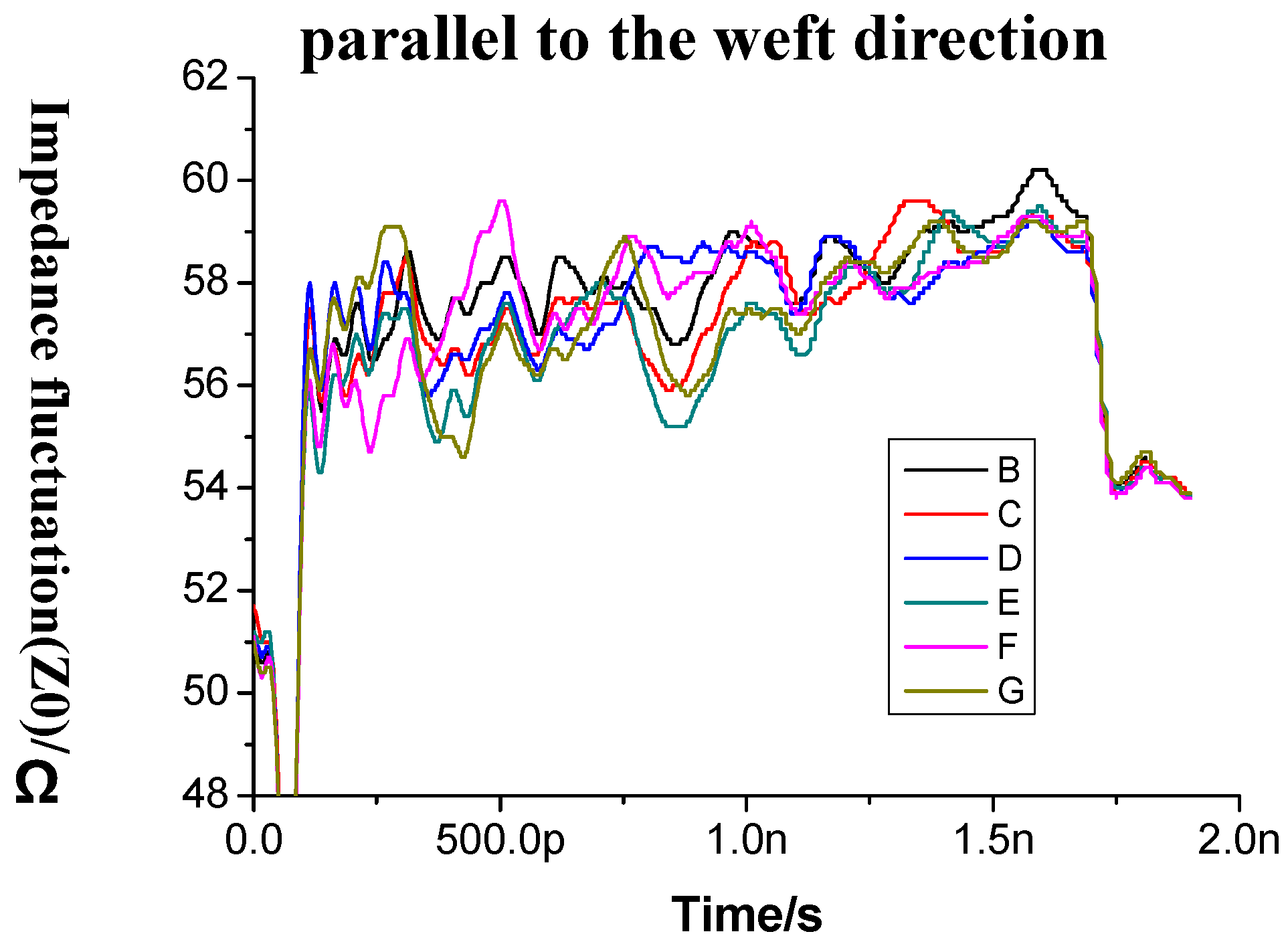
3.2.1. Effect of the Fiber Weave Effect on Single-Ended Impedance Lines

Single-ended impedance is affected by location distribution. Thus, when the Dk exhibited a cyclical variation with the location distribution, it was reflected on the single-ended impedance TDR curves. The effect of fiber weave style on single-ended impedance fluctuation is shown in Figure 6. It was found that 1035 and 1078 had relatively lower impedance fluctuation amplitudes, whereas 1080, 3313, and 2116 had relatively higher impedance fluctuation amplitudes. Here, 1078 and 1035 had the lowest impedance fluctuation amplitudes, below 1.0 Ω for 50 Ω designed traces, whereas for other styles of fiber weave, impedance fluctuation amplitudes could reach 2.0–2.5 Ω. After flattening treatment, the medium homogeneity of 1078 and 1035 was better than the traditional style of fiber weave. The test results were consistent with theoretical calculations.

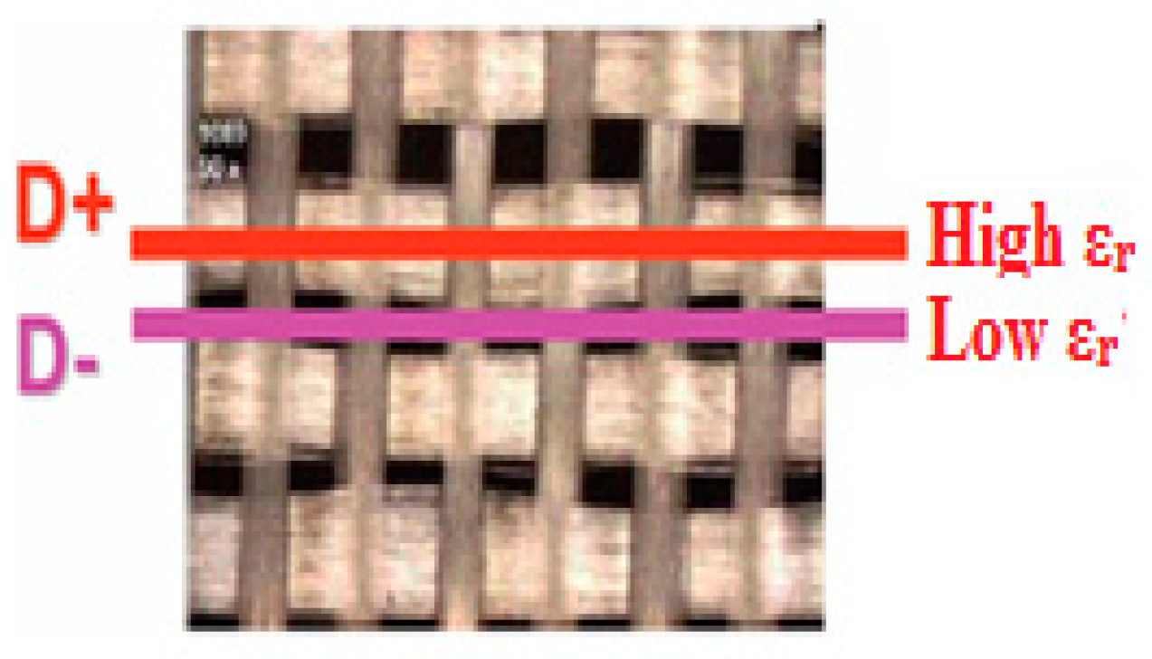
3.2.2. Effect of the Fiber Weave Effect on Differential Lines

Differential lines are shown in Figure 7 and were made up of two halves of differential pairs (designated “D+” and “D−”). They ran over different media (resin vs fiber weave) (see correspondingly different Dk values) and had different propagation properties, especially velocity. It can be concluded that the signal propagation velocities of the two halves of the differential pairs in Figure 7 were different, which resulted in impedance fluctuations of differential lines. We can also call these impedance fluctuations differential skew.
The calculation method of differential skew is shown in Equation (1) [8]. It is the two lines’ propagation delay (tpd1 is the propagation delay of one line of the differential pairs, and tpd2 is another line):
Skew = |tpd1 − tpd2|.
For a microstrip differential line, the propagation delay (tdp) can be calculated using Equation (2) [2]:
tpd = 85*(0.475Dk + 0.67)1/2.
In Equation (2), Dk is the medium dielectric permittivity, and tpd is strongly related to Dk.
Because the laminate was not a homogeneous medium, when a transmission line walked in a different place, the effective dielectric permittivity of the medium was different. The medium dielectric permittivity (Dk) for a specific transmission line (see Figure 8) could be calculated using Equation (3), where εG is the dielectric permittivity of the fiber weave, Dk is the dielectric permittivity of the resin, and H is the total thickness of the fiber weave and resin:
ε = {0.5*εG*W*(H1 + H2)*0.6 + Dk*W*[H − 0.3*(H1 + H2)]}/W/H
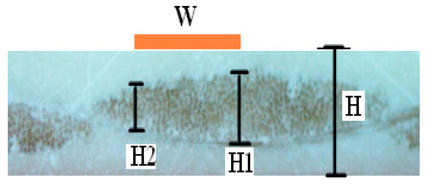
= {0.3*εG*(H1 + H2) + Dk*[H − 0.3*(H1 + H2)]}/H.
According to Equations (1)–(3), we could calculate the maximal differential skew for different styles of single fiber weaves with various differential transmission lines (see Table 2). As can be seen from the table, for some designed transmission lines, the line was big enough to have a fatal influence on the high-speed signal transmission. In addition, skew values were influenced by the designed line’s width and space (W/S). It was found that theoretical line values were close to zero in special situations. This happened when (W+S) equal to X3 or Y3. This is attributed to the fact that the two lines of a differential pair had the same relative location to fiber weave bundles under this situation, and the effective Dk of the two lines was the same. Since it was difficult for designers to obtain detail data of the fiber weave and other functional design requirements, this method would be difficult to realize.

3.3. Effects of Trace Direction on Impedance Fluctuation

Figure 9 and Figure 10 show the effects of trace direction on impedance fluctuation for the 1035 fiber weave. As can be seen from the tested TDR response, the impedance fluctuation amplitude of the warp direction was relatively higher than that of the weft direction. This can be explained with the data in Table 1 and Table 3. In the weft direction, the fiber weave bundles were thinner and better flattened, and the medium homogeneity was better. Thus, for high-speed PCB designing and manufacturing, especially 25-Gbps backplanes, long signal traces should be parallel to the weft direction [8,9].

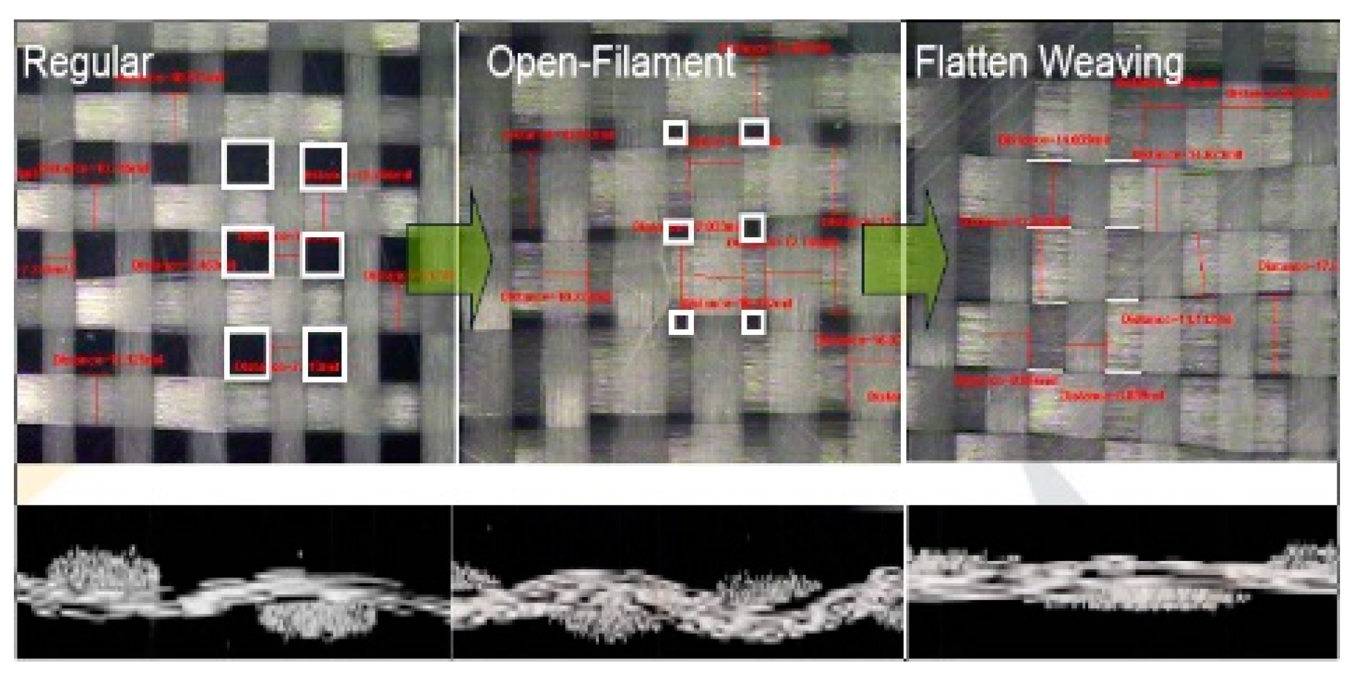
3.4. Methods to Improve Fiber Weave Effects

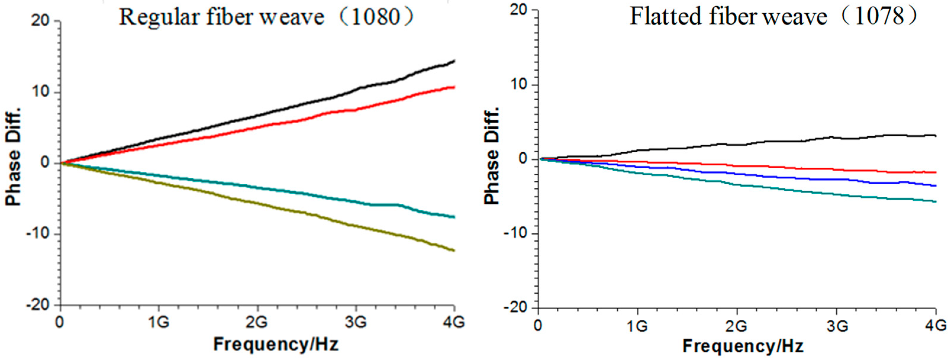
3.4.1. Flattened Fiber Weaves

Flattened fiber weave is a type of fiber that is treated by open-filament or flatten-weave technology. Figure 11 shows the differences in the two styles of fiber weave: Compared to regular glass fiber cloth, flattened fiber weave is more dispersed, the dielectric uniformity is better, and the difference in the dielectric constant between the differential lines becomes smaller.
The properties of fiber weaves could be expressed by a phase differential (∆Phase), which is the propagation delay at different transmission frequencies (see Equation (4)), and we could use a vector network analyzer to detect ∆Phase.
The ∆Phase of 1078 (a type of flattened fiber weave) was much lower than that of 1080 (a type of normal fiber weave) (Figure 12). This means that a flattened fiber weave can improve a PCB’s signal transmission quality. According to Equation (4), the skew values of the 1080 and 1078 fiber weaves can be obtained (4 ps/in. and 2 ps/in., respectively). Thus, for a 25-Gbps PCB, especially a backplane, a flattened fiber weave is often used for stack-up. In recent years, flattened fiber weaves have been widely used in high-speed laminates, and traditional 106 and 1080 fiber weaves have been abandoned in the Megtron 7.
∆Phase = Skew* Frequency *360.

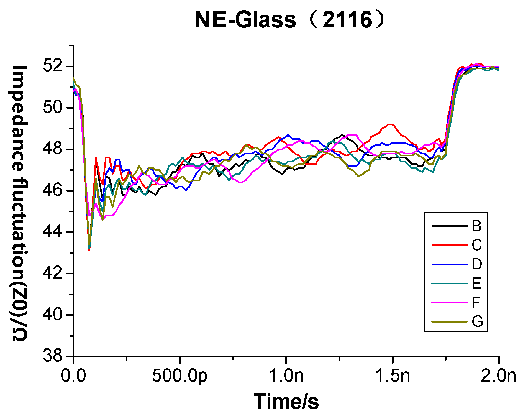
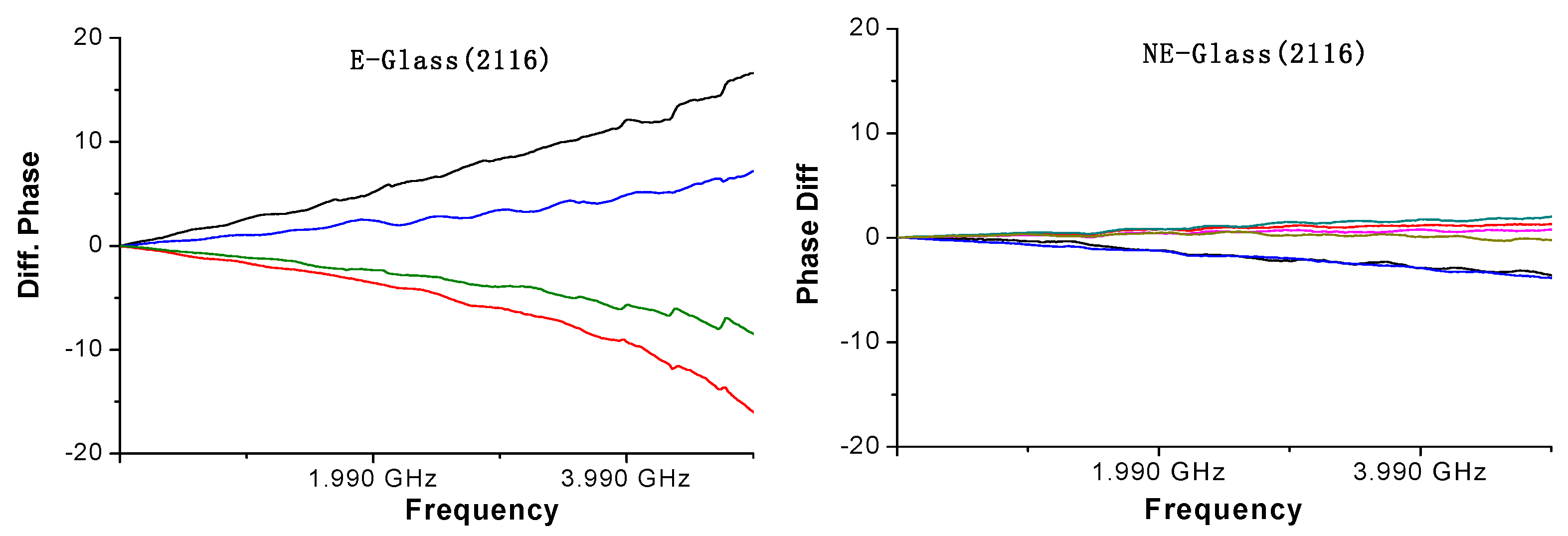
3.4.2. NE-Glass Fiber Weaves

NE-glass (new electronic glass), a product of Nittobo, shows improved electrical and mechanical performance over traditional E-glass and is widely used in some low-loss laminate products (for example, it was used in Nelco’s N4000-13 SI and Meterowave 2000, TUC’s TU872 SLK SP, and Panasonic’s Megtron 6 NE and Megtron 7NE). NE-glass shows better temperature stability, lower Dk, and lower loss than the equivalent E-glass. The reduced Dk of NE-glass yields important benefits for high-performance signaling applications [10]. Materials that using NE-glass have less variation between the Dk of resin. With a ratio of glass/PPO resin as 46:54, we could calculate the nominal laminate Dk to be 3.6 with E-glass, but with NE-glass would be 3.35.
Figure 13 shows the impedance fluctuation (Z0) of traces routed on NE-glass. When compared to Figure 7 and Figure 8, it was found that traces routed on NE-glass showed much lower impedance fluctuations (Z0).
Figure 14 shows phase differentials for differential pairs produced with NE-glass and E-glass. The results indicated that the ∆Phase of NE-glass was much lower than that of E-glass. Due to its excellent performance, NE-glass has been widely used in low-loss, very low-loss, and ultralow-loss laminates.

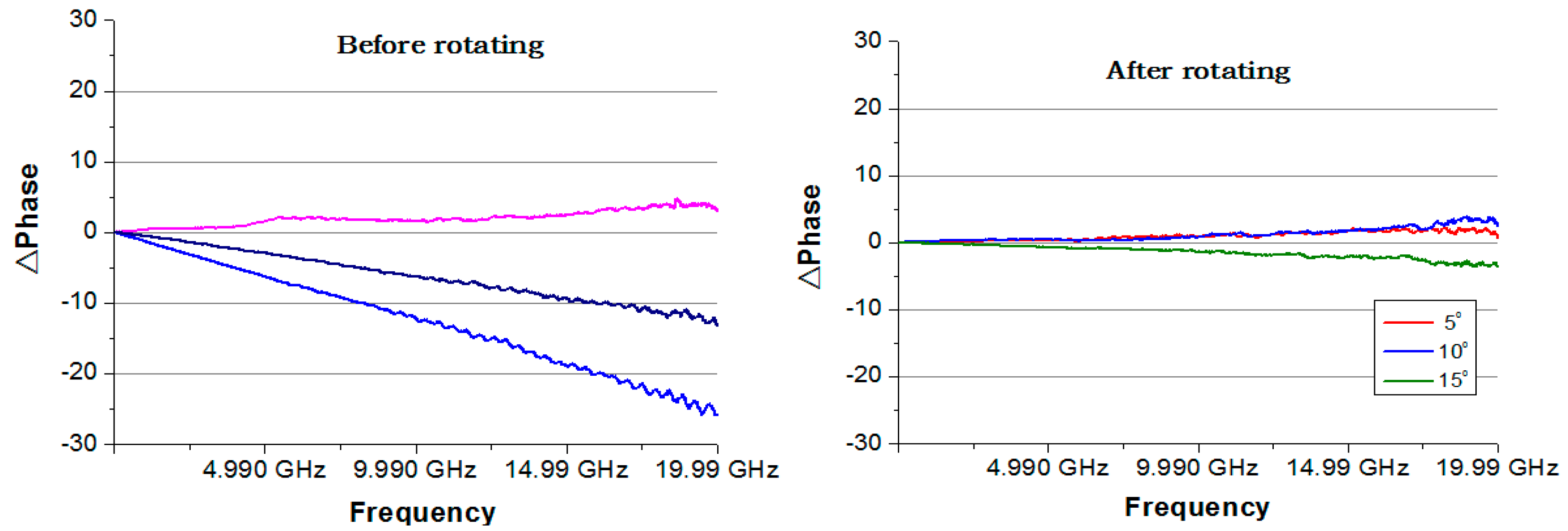
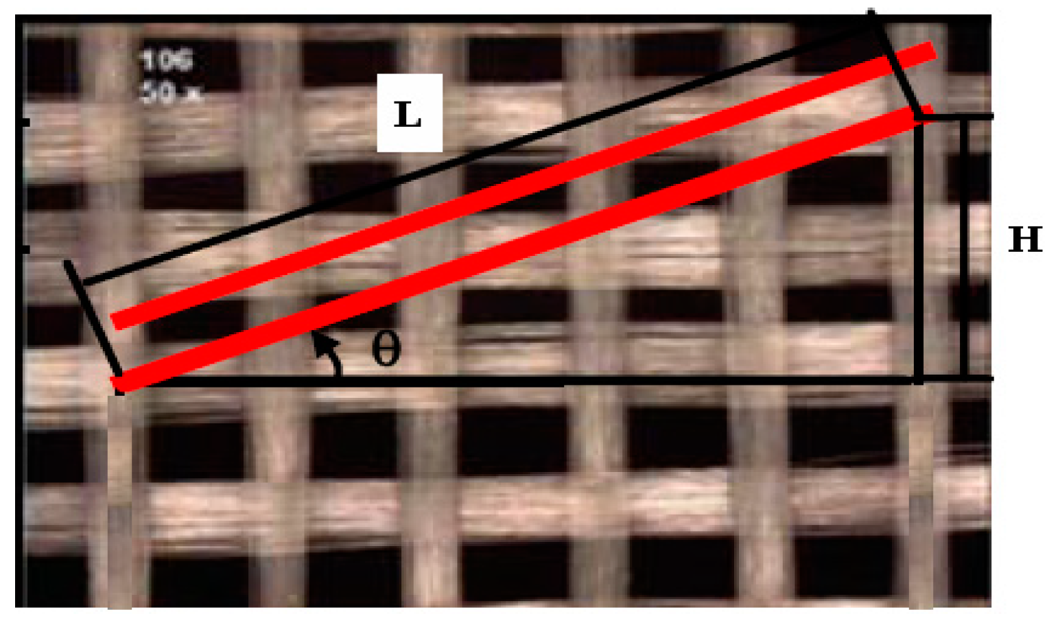
3.4.3. Making Traces and Fiber Weave Bundles with an Angle

Making signal traces and fiber weave bundles with an angle is a relatively simple and effective method to solve the differential skew problem [11,12]. There are two practical methods to achieve this:
(1) The PCB manufacturer rotates the image. This reduces the utilization rate of laminates and increases production costs. Usually, a 10 degrees rotation angle makes production costs increase 8–10%. For customers, this is a big increase;
(2) The designer rotates the trace. This approach requires designers to rotate the signal trace during layout. This would increase the difficulty of layout and affects layout efficiency.
Another question is what is the right angle. Here, we tested the effects of three kinds of rotation angles (5 degrees, 10 degrees, and 15 degrees). As can be seen from Figure 15, the ∆Phase results of the three kinds of rotation angles were basically identical. This means it did not take too much of an angle between trace and fiber weave bundle to resolve the fiber weave problem. Theoretically, a trace merely has to cross two weave bundles along its length, so that the effect on the two adjacent traces is equalized (see Figure 16 and Equation (5)) [1]. According to the pitch size of the fiber weave bundles and trace lengths, the rotation angle could be calculated.

4. Conclusions

The dielectric constant fluctuation of different types of fiber weaves were inconsistent: 1080, 3313, and 2116 are much larger than 1035 and 1078 (1080 is 0.44 and 1078 is 0.18). This fluctuation characteristic fed back to the effect on impedance and signal propagation delay. Here, 1035 and 1078 had relatively lower impedance fluctuations, which were below 1.0 Ω for 50 Ω designed traces (1080, 3313, and 2116 could reach 2.0–2.5 Ω), and lower differential skews with various differential transmission lines (1078 was 2 ps/in. and 1080 could reach 4.0 ps/in.).
For methods to improve the fiber weave effect, we advise high-speed digital designers to use flattened fiber weaves (such as 1078 and 1035) and NE-glass fiber weaves (such as 2116NE). We also suggest designing long signal lines parallel to the weft direction or rotating the image with a proper angle (if the fiber weave pitch is not known, 5 degree is recommended).

Author Contributions

B.C. makes substantial contributions to conception and design, acquisition of data, analysis and interpretation of data; R.Y. gives final approval of the version to be submitted and any revised version; H.W. participates in drafting the article or revising it critically for important intellectual content; K.G. participates in drafting the article or revising it critically for important intellectual content; J.L. submit this article.

Funding

This work was supported by the Science and Technology Project of Guangdong (2014B090901017) and the Science and Technology Project of Guangzhou (201604010086).

Conflicts of Interest

The authors declare no conflicts of interest.

References

  1. Dudek, R.; Goldman, P.; Kuhn, J. Advanced Glass Reinforcement Technology for Improved Signal Integrity. Printed Circuit Design & Fab. 2008, pp. 40–42. Available online: https://www.pcdandf.com/pcdesign/index.php/articles-by-subject/210-signal-integrity/3378-advanced-glass-reinforcement-technology-for-improved-signal-integrity (accessed on 20 January 2018).
  2. Scott, M.; Chris, H. The impact of PCB laminate weave on the electrical performance of differential signaling at multi-Gigabit data rates. In Proceedings of the Design Conference, Santa Clara, CA, USA, 31 January 2005. [Google Scholar]
  3. Cai, J.Q. PCB used layer insulation film and high function glass cloth Printed Circuit Information. Circuit Inf. 2011, 12, 26–31. [Google Scholar]
  4. Avendano, V.; Champac, V.; Figureas, J. Signal integrity verification using high speed monitors. In Proceedings of the European Test Symposium, Corsica, France, 23–26 May 2004; pp. 114–119. [Google Scholar]
  5. Loyer, J.; Kuuze, R.K.; Ye, X.N. Fiber Wave Effect: Fiber Weave Effect: Practical Impact Analysis and Mitigation Strategies. In Proceedings of the Design Conference, Santa Clara, CA, USA, 29 January–1 February 2007. [Google Scholar]
  6. Sharawi, M.S. Practical Issues in High Speed PCB Design. Potentials IEEE 2004, 23, 24–27. [Google Scholar] [CrossRef]
  7. Jiang, L.H.; Zhu, Y.H.; Zhang, N.; Zhuo, N.Z.; Xing, H.D.; Wang, H.B. The Research of the Low Dielectric Properties of Fiberglass and the Application of Fiberglass in High Frequency Printed circuit Board. Fiber Glass 2016, 3, 1–6. [Google Scholar]
  8. Bucur, D. Fiber Weave Effect—A performance-limiting factor. In Proceedings of the International Conference on Communications, Bucharest, Romania, 29–31 May 2014; pp. 1–4. [Google Scholar]
  9. Zhang, T.; Chen, X.; Schutt-Aine, J.E.; Cangellaris, A.C. Statistical analysis of fiber weave effect over differential microstrips on printed circuit boards. Signal Power Integr. 2014, 40, 1–4. [Google Scholar]
  10. Luevano, G.R.; Shin, J.; Michalka, T. Practical Investigations of Fiber Weave Effects on High-speed Interfaces. In Proceedings of the IEEE Electronic Components & Technology Conference, Las Vegas, NV, USA, 28–31 May 2013; pp. 2041–2045. [Google Scholar]
  11. Shlepnev, Y.; Nwachukwu, C. Modelling Jitter Induced by Fibre Weave Effect in PCB Dielectrics. In Proceedings of the IEEE International Symposium on Electromagnetic Compatibility, Raleigh, NC, USA, 4–8 August 2014; pp. 803–808. [Google Scholar]
  12. Cao, Y.; Li, J.; Hu, J.; Zheng, M. Design Consideration for 10 Gbps Signal Transmission Channel in Copper Backplane System. In Proceedings of the International Conference on Computational Science & Its Applications, Santander, Spain, 20–23 June 2011; pp. 215–218. [Google Scholar]
Figure 1. The graphic design of the Dk test.
Applsci 09 00353 g001
Figure 2. The Dk variation due to fiber weave.
Applsci 09 00353 g002
Figure 3. Photos to illustrate fiber weave bundle parameters.
Applsci 09 00353 g003
Figure 4. The Dk fluctuation amplitude parallel to warp direction.
Applsci 09 00353 g004
Figure 5. The Dk fluctuation amplitude parallel to weft direction.
Applsci 09 00353 g005
Figure 6. Effect of fiber weave style on impedance fluctuation.
Applsci 09 00353 g006
Figure 7. Photos to illustrate differential lines.
Applsci 09 00353 g007
Figure 8. Photos to illustrate the Dk calculation.
Applsci 09 00353 g008
Figure 9. Impedance fluctuation of traces parallel to the warp direction.
Applsci 09 00353 g009
Figure 10. Impedance fluctuation of traces parallel to the weft direction.
Applsci 09 00353 g010
Figure 11. The structure of regular weaves and flattened fiber weaves.
Applsci 09 00353 g011
Figure 12. ∆Phase of regular and flattened fiber weaves.
Applsci 09 00353 g012
Figure 13. Impedance fluctuation of traces on NE-glass.
Applsci 09 00353 g013
Figure 14. ∆Phase of Electronic-glass versus NE-glass.
Applsci 09 00353 g014
Figure 15. ∆Phase before and after rotating.
Applsci 09 00353 g015
Figure 16. Calculation of the rotation angle.
Applsci 09 00353 g016
Table 1. Measurement results of fiber weave bundle parameters.
StyleMeasurement Results (mil)
X1X2X3Y1Y2Y3
10350.828.814.20.7812.413.7
10801.68.217.01.112.122.4
10781.414.216.21.017.617.8
33131.913.116.21.511.016.3
21162.214.117.22.015.517.3
Table 2. Maximal differential skew for different styles of fiber weave.
W/S (mil)Differential Skew (ps/in)
10351080331321161078
WeftWarpWeft Warp Weft Warp Weft Warp Weft Warp
4/44.73.57.25.16.33.16.44.62.81.9
4/80.90.46.55.16.51.32.63.62.21.6
5/54.32.36.64.77.35.65.14.82.72.0
5/90.40.35.04.73.01.81.01.21.21.1
6/60.90.45.24.65.74.13.43.32.31.5
6/80.00.02.84.33.52.21.21.41.50.8
7/70.00.01.74.02.72.60.61.11.00.7
7/90.40.30.83.90.80.80.10.10.20.1
8/80.70.40.43.10.40.90.00.30.10.3
8/101.871.470.31.90.00.50.80.00.10.0
Table 3. Variations in warp and weft directions of different fiber weave types.
Fiber Weave StyleWarp DirectionWeft Direction
∆Dk∆Z0/Ω∆Dk∆Z0/Ω
Conventional fiber weave0.583.800.44 2.73
Flattened fiber weave0.25 1.560.18 1.11

