Article

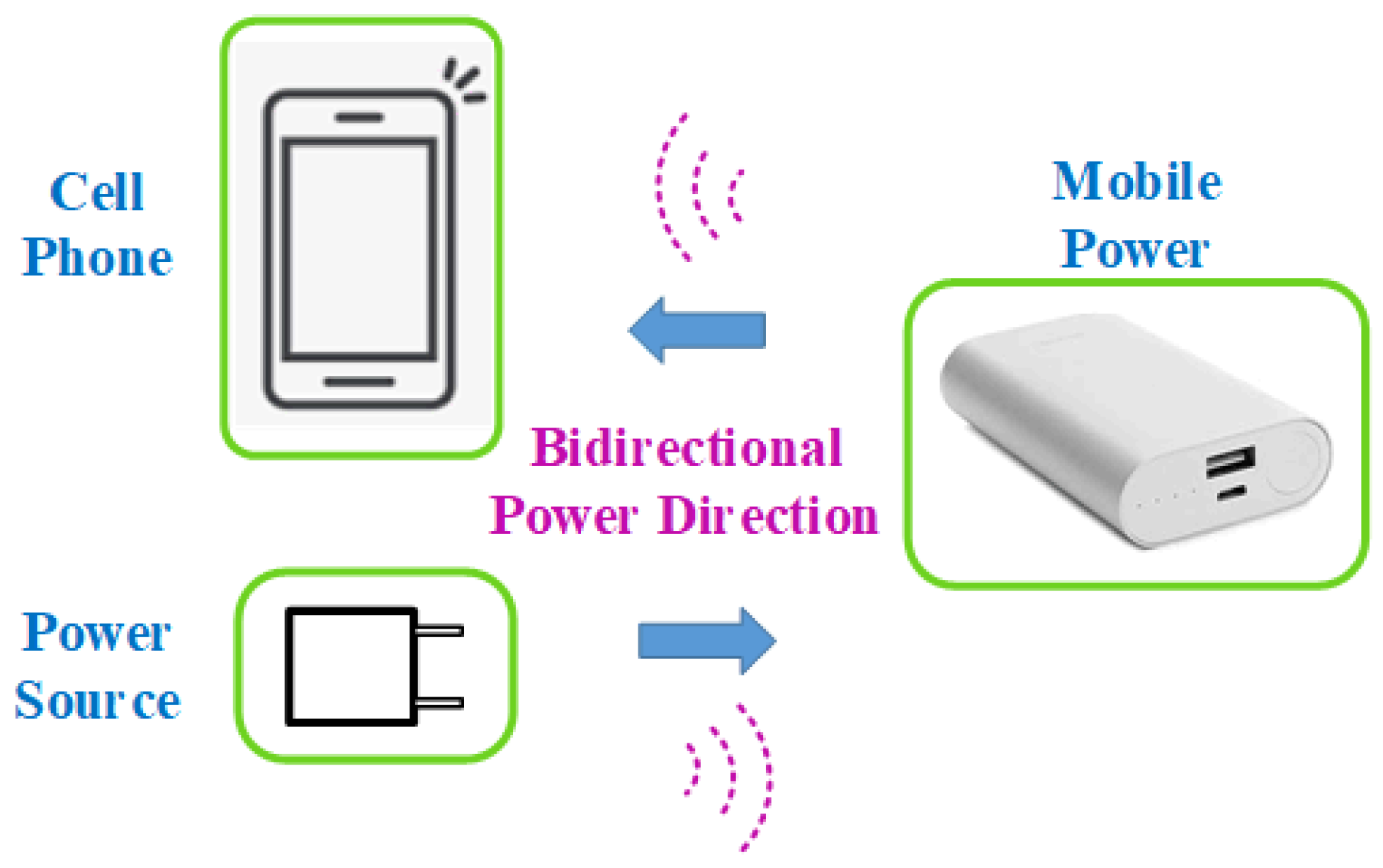
A Novel Bidirectional Wireless Power Transfer System for Mobile Power Application

Department of Electrical Engineering, National Central University, Taoyuan City 320, Taiwan
*
Author to whom correspondence should be addressed.
Appl. Sci. 2019, 9(18), 3769; https://doi.org/10.3390/app9183769
Submission received: 28 July 2019 / Revised: 6 September 2019 / Accepted: 6 September 2019 / Published: 9 September 2019
(This article belongs to the Special Issue Intelligent System Innovation)

Abstract

:

Featured Application

The proposed system is suitable for low power applications such as a mobile power source used in wearable smart devices or sensor devices.

Abstract

This paper presents a bidirectional wireless power transfer system for mobile power applications. A novel 2-switch bidirectional wireless power transfer system with dual-side control is proposed for mobile power applications. Although only two switches are adopted, the energy can be transferred from the transmitter side to the receiver side and vice versa. The term bidirectional means that the power-flow is bidirectional and also that the transmitter is also a receiver and the receiver is also a transmitter. The output energy can be easily controlled by the duty ratios of the two switches. Thus, the proposed bidirectional power transfer system uses only one circuit to achieve bidirectional power transfer. Hence, the system cost and volume can be reduced so that the system is small and convenient for mobile power systems, portable and/or wearable electronic devices. A prototype system is constructed and the experimental results verify the validity of the proposed bidirectional wireless power transfer system.

1. Introduction

Wireless power transfer systems have been studied by many researchers due to the system merits (WPT) such as cordless, wireless charging and safety in power transfer [1,2,3,4,5,6]. Wireless power transfer has been applied to many applications including high power applications such as electric vehicle (EV) chargers and low power applications such as mobile power systems, intelligent mobiles, wearable electronic devices and sensors, etc. There are critical issues to be overcome in the practical design of wireless power transfer systems. One of the issues is the position and shape of the magnetic coupler. The most commonly used magnetic coupler structures in wireless charging are the circular and rectangular types. Based on the magnetic dipole moment theory, the magnetic dipole moment is proportional to the current magnitude and current loop area. Hence, the larger the current loop area is, the larger the magnetic dipole moment. Therefore, if the circular diameter is the same as the length and width of the rectangle, the rectangular type area is larger than 1.27 times the area of the circular type. Some literatures [7,8] discussed the shape of the inductive coupler and coupler array to generate better magnetic dipole moment to induce the desired energy.
In order to wirelessly deliver the energy from one side to the other side, except considering the magnetic coupler position and shape, the wireless converter design for different applications is also very important. Figure 1 shows a full-bridge bidirectional wireless power transfer EV charger system [9,10,11,12]. The system can transfer energy from the grid to the vehicle (G2V) as well as transfer energy from the vehicle to the grid (V2G) [12,13,14,15,16]. In this case the EV can be seen as an energy storage system that provides active power or reactive power to the grid whereas renewable energies such as solar energy or wind power are all in the power system. Bidirectional WPT is needed as well as unidirectional power transfer [16]. Beyond the magnetic coupling and WPT circuit, the closed-loop control schemes are also essential to realize the WPT converter function. Closed-loop control schemes can be classified into three control types, including transmitter-side control [17], receiver-side control [18,19], and dual-side control [20]. Receiver-side control is better than transmitter-side control and dual-side control in maintaining the load requirement. The dual-side control is apparently more important for bidirectional power flow control.
A novel bidirectional WPT converter with only two switches is introduced in this paper. Dual-side control is also proposed for bidirectional power flow. Compared with the 8-switch full bridge bidirectional WPT converter, as shown in Figure 1, which is often utilized in the EV charger system, the proposed 2-switch bidirectional WPT converter is more suitable for mobile power systems, portable and/or wearable electronic devices with low power applications. Figure 2 demonstrates the cell phone power supply using mobile power with wireless power transfer technology for charging and discharging. Up to now, there is usually unidirectional wireless power transfer application in the mobile power supply. A bidirectional wireless power transfer technology for low power applications using simple circuitry with only two switches is proposed.

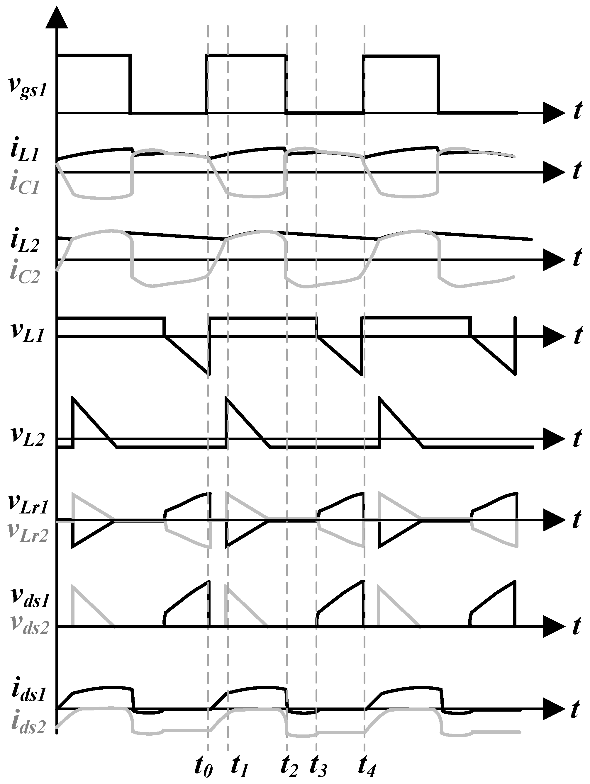
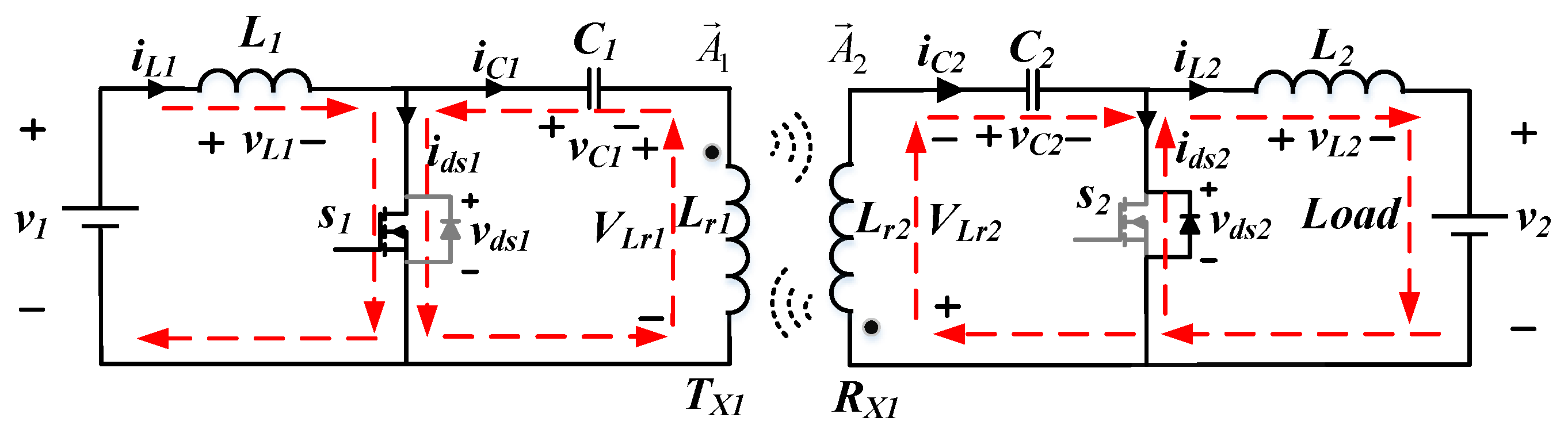
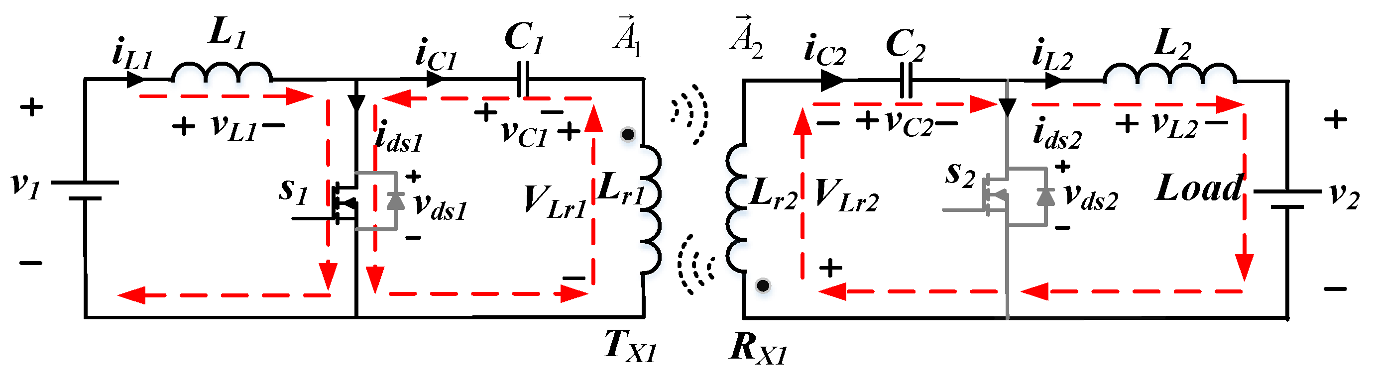
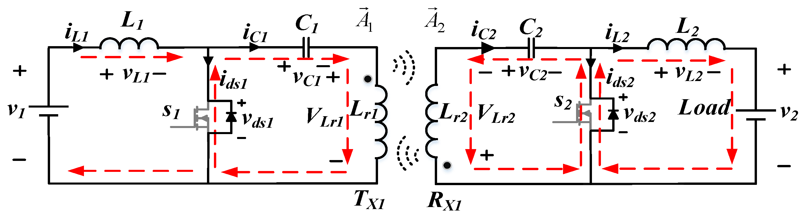
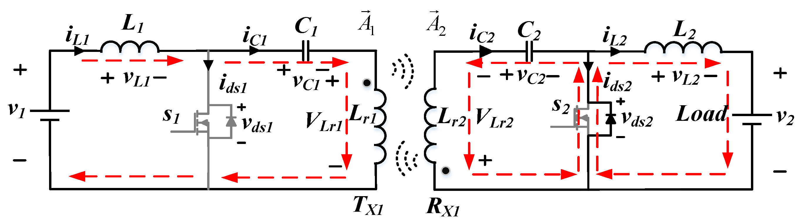
2. Analysis of Proposed Circuit Topology

The proposed bidirectional wireless power transfer circuit with primary side and secondary side circuits is shown in Figure 3. Both the primary side and secondary side circuits can be the transmitter (TX) or receiver (RX). In the proposed topology, there is a boost inductor, an active switch, as well as a resonant capacitor and resonant coupled inductor in both the primary side and secondary side. The primary side circuit and secondary side circuit are designed to be symmetric to each other. However, the power direction is controlled by the switching duty ratios D1 and D2 of switch 1 and switch 2. While switch 1 is active and switch 2 is idle, the power flow is controlled from Tx1 to Rx1. While switch 2 is active and switch 1 is idle, the power flow is controlled from Tx2 to Rx2. Therefore, the energy can be transferred easily from primary side to the secondary side or from secondary side to the primary side.
For convenient explanation of how the circuit works, assume that the primary side is the transmitter and the secondary side is the receiver. The active switches are assumed to be ideal active switches with anti-paralleling body diode. To illustrate the circuit operation, the key waveforms of the proposed bidirectional wireless power transfer system during one switching period are shown in Figure 4 and the circuit operation can be divided into four states to explain and discuss.
(1) State 1 (t0t <t1): In this mode, as shown in Figure 5, the switch S1 is turned on and switch S2 is turned off as be a diode. Switch current ids1 is increasing. Inductor L1 is magnetized by the input voltage V1 so as to increase the inductor current iL1. The capacitor C1 resonates with the coupled inductor Lr1. The resonant current ic1 is changed from positive to negative and produces the magnetic vector potential A 1 through the primary side plane coil, i.e., the transmitter. The magnetic vector potential A 1 is transmitted to the secondary side plane coil, i.e., the receiver and generates a resonance between the Lr2 and C2 so as to release energy to the inductor L2 and load. The equivalent circuit equations can be described as Equations (1)–(6).
L 1 d i L 1 d t = v 1 ,
L r 1 d i L r 1 d t + M d i L r 2 d t = v C 1 ,
C 1 d v C 1 d t = i L r 1 ,
C 2 d v C 2 d t = i L r 2 ,
L r 1 d i L r 1 d t + M d i L r 2 d t = v C 2 ,
L 2 d i L 2 d t = v 2 ,
where M is the mutual inductance and determined by the magnetic vector potential A 1 and A 2 . Therefore, the mutual inductance can be expressed as M = μ 0 N 1 N 2 4 π C 2 C 1 d l 1 d l 2 R . N1 and N2 are the numbers of turns of the primary and secondary side, respectively. l 1 and l 2 indicate the flux direction of coil 1 at primary side and coil 2 at secondary side, respectively. R is the distance between the primary-side and secondary-side windings.
(2) State 2 (t1t <t2): In this mode, as shown in Figure 6, switch S1 is turned on and switch S2 is turned off. Switch current ids1 is increasing. Inductor L1 is magnetized by the input voltage V1 so as to increase the inductor current iL1. The capacitor C1 resonates with the coupled inductor Lr1 and the current ic1 is negative. However, VLr1 changes from zero to negative and VLr2 changes from zero to positive. The magnetic vector potential A 1 is transmitted from the primary side to the secondary side and generates a resonance between the Lr2 and C2 that releases energy to inductor L2 and the load. The current iC2 is positive. The equivalent circuit equations can be expressed as Equations (7)–(12).
L 1 d i L 1 d t = v 1 ,
L r 1 d i L r 1 d t + M d i L r 2 d t = v C 1 ,
C 1 d v C 1 d t = i L r 1 ,
C 2 d v C 2 d t = i L 2 ,
L r 2 d i L r 2 d t + M d i L r 1 d t = v 2 v L 2 v C 2 ,
L 2 d i L 2 d t = v L r 2 v C 2 v 2 ,
(3) State 3 (t2t <t3): In this mode, as shown in Figure 7, switch S1 is turned off and S2 is also turned off. Ids1 current is negative. Inductor L1 is magnetized by the input voltage V1 so as to increase the inductor current iL1. However, ic1 is changed from negative to positive and ic2 is changed from positive to negative. The magnetic vector potential A 1 produced by the primary side plane coil is transmitted from the primary side to the secondary side and releases energy to inductor L2 and the load. The equivalent circuit equations can be described as Equations (13)–(18).
L 1 d i L 1 d t = v 1 ,
L r 1 d i L r 1 d t + M d i L r 2 d t = v C 1 ,
C 1 d v C 1 d t = i L r 1 ,
C 2 d v C 2 d t = i L r 2 ,
L r 2 d i L r 2 d t + M d i L r 1 d t = v C 2 ,
L 2 d i L 2 d t = v 2 ,
(4) State 4 (t3t <t4): In this mode, as shown in Figure 8, the switches S1 and S2 are turned off. Ids1 is zero, and ic1 still remains positive and ic2 still remains negative. The magnetic vector potential A 1 is transmitted from primary side to the secondary side and generates a resonance between the Lr2 and C2 so as to release the energy to inductor L2 and load. The current ids2 remains the negative current to provide the load positive current. The equivalent circuit equations can be expressed as Equations (19)–(24).
L 1 d i L 1 d t = v 1 v C 1 v L r 1 ,
C 1 d v C 1 d t = i L 1 ,
L r 1 d i L r 1 d t + M d i L r 2 d t = v 1 v C 1 v L 1 ,
C 2 d v C 2 d t = i L r 2 ,
L r 2 d i L r 2 d t + M d i L r 1 d t = v C 2 ,
L 2 d i L 2 d t = v 2 ,

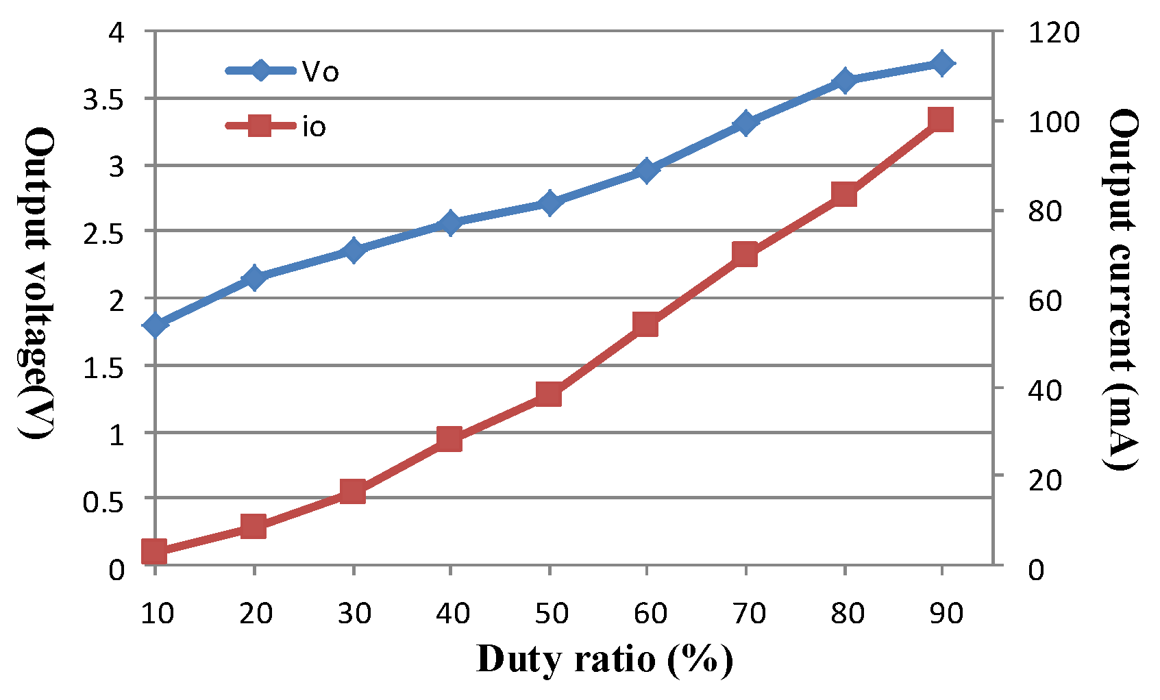
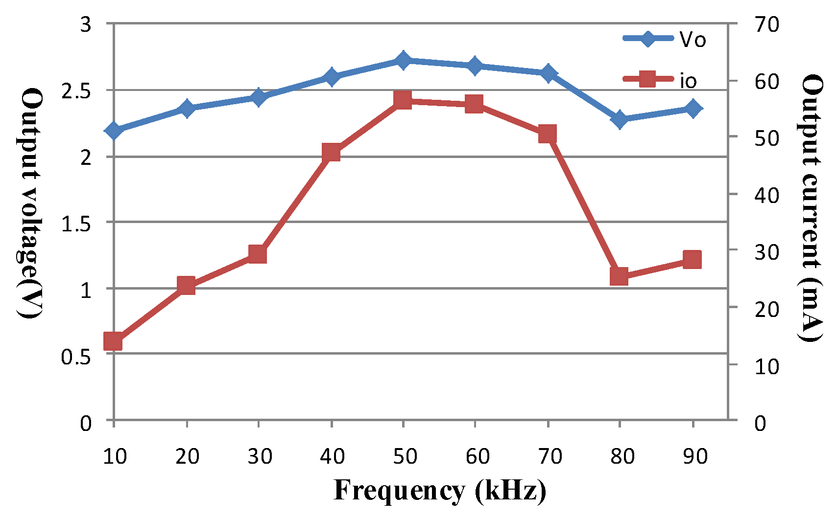
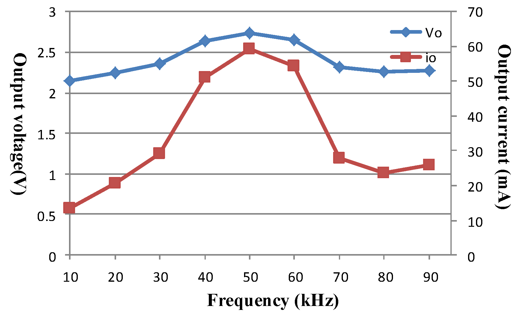
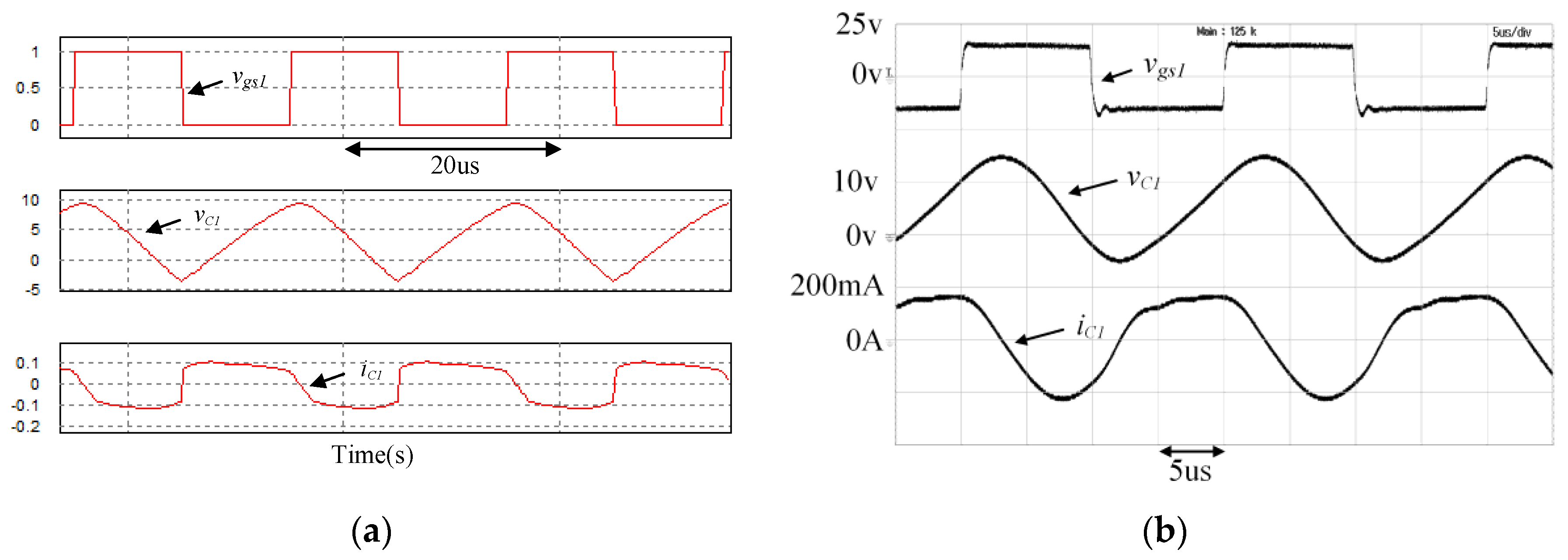
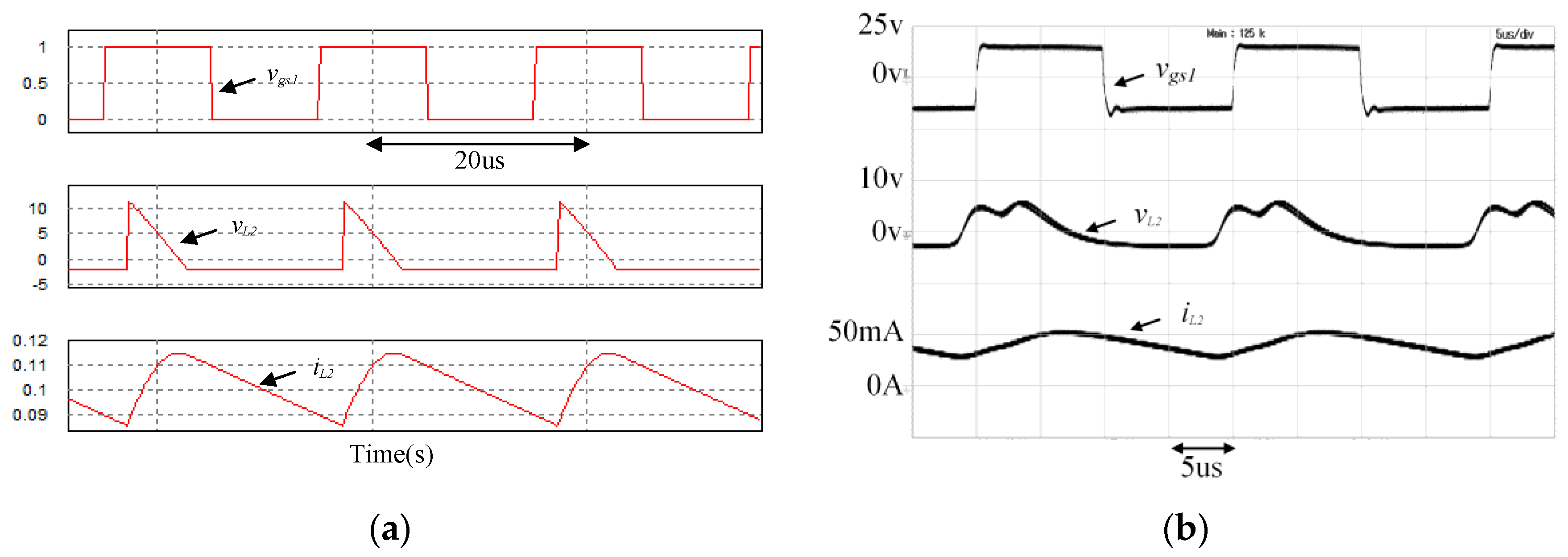
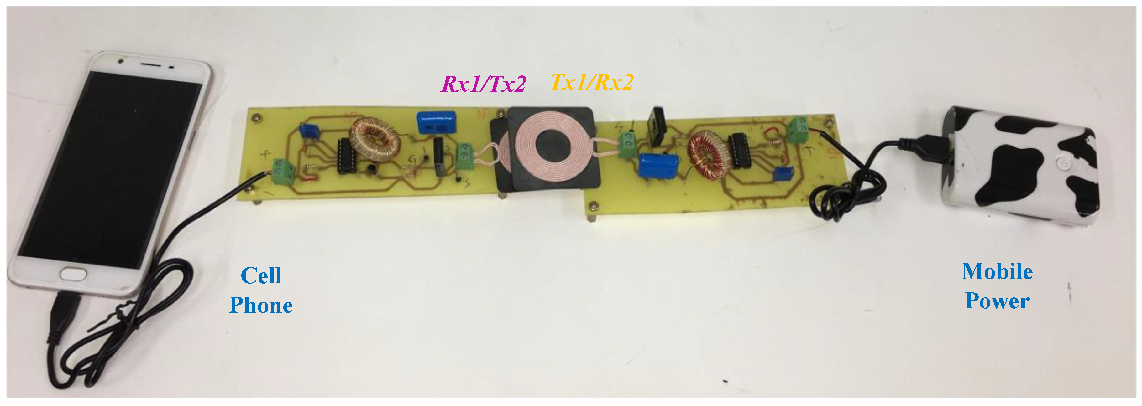
3. Simulation and Experimental Results

To verify the feasibility of the proposed bidirectional wireless power transfer system, the well-known software Power SIM Version 9.0 (Powersim Inc, Rockville, M.D, USA, 2010) is adopted to perform the simulation process. In the simulation, the switches, capacitors and inductors are assumed to be ideal. A transformer with a loosely coupled inductor and relatively larger magnetizing inductor is adopted to simulate the transmitter and receiver.
Meanwhile, a prototype is constructed using a coreless plane transformer to verify the theoretical results. The simulation and experimental parameters for the proposed bidirectional wireless power transfer system are listed in Table 1. Where the LED load is adopted to emulate the portable device, the mobile power supply is used to provide 5V voltage source. The transmitter and receiver coils are the same type and the photo is shown in Table 1 with a detailed description. The instantaneous current and voltage in experiment are measured by the oscilloscope YOKOGAWA DLM2024.
The simulation and experimental results of resonant capacitor voltage Vc1 and current ic1 with the corresponding control switching signal are shown in Figure 9a,b, respectively. As can be observed from Figure 9, the capacitor voltage Vc1 and current ic1 are resonated following the switching frequency. One can see that both the simulation and experimental results are in very close agreement. Figure 10a shows the inductor voltage VL2 and current iL2 simulation results with the corresponding control switching signal. The corresponding experimental results are shown in Figure 10b. As can be seen from Figure 10, the inductor L2 stabilizes the output current. Although the simulation and experimental waveforms of VL2 and iL2 have something different due to the parasitic effects, the simulation and experimental behavior are very similar. The inductor voltage VL1 and current iL1 simulation and experimental results with the corresponding control switching signal are shown in Figure 11a,b. From Figure 11, one can find that both the simulation and experimental results are in very close agreement.

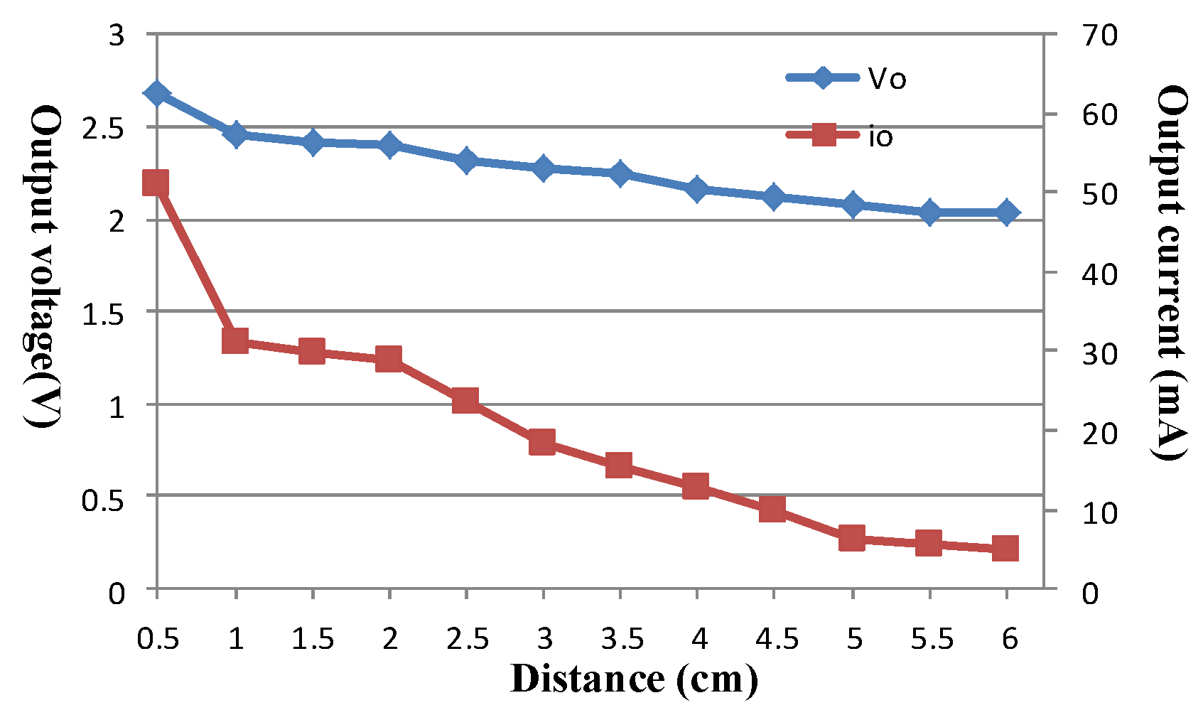
4. System Analysis and Discussion

With the aforementioned understanding of the proposed circuit operation principle and the circuit equivalent models, it is now straightforward to test and measured the proposed contactless bidirectional power transfer system in the experiments. The bidirectional power flow with dual-side duty ratio control will be tested and explained here. For convenient explanation, while the power is delivered form primary side to secondary side, one can call it forward mode operation. While the power is delivered from secondary side to the primary side, one can call it backward mode operation. In the proposed system the forward mode operation is controlled by the switch S1 duty ratio and the backward mode operation is controlled by the switch S2 duty ratio. The power flow direction can be controlled by the switch duty ratio always in the transmitter side.
The averaged output voltage and output current values are recorded in this section and measured by the oscilloscope YOKOGAWA DLM2024. The duty ratio control for forward mode and backward mode operation test results are shown in Figure 12; Figure 13, respectively. As can be observed from Figure 12; Figure 13, the output voltage and current can be controlled almost linearly by the duty ratio and the maximum output power point is at the 0.9 duty ratio, regardless whether the circuit is operated in the forward or backward mode. This represents that the system output power can be obviously and easily adjusted to increase or decrease for applications.
The switching frequency variation test results for forward and backward mode operations are shown in Figure 14; Figure 15, respectively. The circuit resonant frequency is designed at 50 kHz and the measured optimal switching frequency is also located at 50 kHz. If the switching frequency is between 40 kHz and 60 kHz near the resonant frequency, the output voltage and current are not seriously affected in the proposed circuit. This means that the resonant capacitor and/or resonant inductor value variation in the system due to the environment causing resonant frequency offset is easily corrected by properly adjusting the switching frequency. To explain how the distance between the windings affects the power transfer, Figure 16; Figure 17 show the output voltage and current vs. distance in the forward mode and backward mode operations, respectively, where there is 180-degree direction in coil 2 compared to coil 1 which has 0-digree direction. Coils 1 and 2 are overlapped with distance R. As can be observed from Figure 16; Figure 17, the voltage and current are decayed with increasing distance R and the magnetic vector potential A is decayed with the rate proportional to 1 / R 2 . The measured power conversion efficiency is about 50%, while the coils are very close to each other.
According to the above test, the proposed wireless power transfer system can transfer the power flow bi-directionally and the output voltage and/or current can be adjusted through the switch duty ratios regardless whether the system is operated in the forward or backward mode. One low-power WPT application for mobile power is shown in Figure 18.

5. Conclusions

This paper proposed a novel wireless bidirectional power transfer system. The circuit operation principle is explained in detail and the equivalent circuits are also derived. The proposed wireless power transfer system can be seen as a bidirectional current-control current-source system. The power flow direction can be controlled using the transmitter side switch. The output voltage and/or current can be controlled using the switch duty ratio regardless whether the proposed system is operating in the forward or backward mode. Fortunately, only two switches are adopted to achieve the bidirectional power flow transmission. Therefore, the proposed converter is suitable for low power applications such as a mobile power source used in wearable smart devices or sensor devices. A prototype system was constructed and tested. Both the simulation and experimental results verify the validity of the proposed bidirectional wireless power transfer system.

Author Contributions

The paper was a collaborative effort between the authors. The authors contributed collectively to the theoretical analysis, modeling, simulation, experiment, and manuscript preparation.

Funding

This research is sponsored by the Ministry of Science and Technology of Taiwan under Grant MOST 108-3116-F-008-001.

Conflicts of Interest

The authors declare no conflicts of interest.

Nomenclature

EVElectric vehicle
WPTWireless power transfer
TxTransmitter
RxReceiver
MMutual inductance
A 1 , A 2 Magnetic vector potential
μ 0 Permeability of vacuum
L1, L2Boost inductor
C1, C2, Cr1, Cr2Resonant capacitor
Lr1, Lr2Resonant coupled inductor
S1, S2Active switch
VgsxGate signal of active switch x, x = 1, 2
V1, V2Voltage sources of primary and secondary side
D1, D2Switching duty ratios of switch 1 and switch 2

References

  1. Nutwong, S.; Sangswang, A.; Naetiladdanon, S. An Inverter Topology for Wireless Power Transfer System with Multiple Transmitter Coils. Appl. Sci. 2019, 9, 1551. [Google Scholar] [CrossRef]
  2. Tao, X.; Rong, C.; Lu, C.; Huang, X.; Zeng, Y.; Hu, Z.; Liu, M. A Novel Approach to Reach Impedance Matching in Wireless Power Transfer Systems. Appl. Sci. 2019, 9, 976. [Google Scholar] [CrossRef]
  3. Li, Z.; Zhu, C.; Jiang, J.; Song, K.; Wei, G. A 3-kW Wireless Power Transfer System for Sightseeing Car Supercapacitor Charge. IEEE Trans. Power Electron. 2017, 32, 3301–3316. [Google Scholar] [CrossRef]
  4. Li, Y.; Grabham, N.; Torah, R.; Tudor, J.; Beeby, S. Textile-Based Flexible Coils for Wireless Inductive Power Transmission. Appl. Sci. 2018, 8, 912. [Google Scholar] [CrossRef]
  5. Matsumoto, H.; Neba, Y.; Ishizaka, K.; Itoh, R. Comparison of characteristics on planar contactless power transfer systems. IEEE Trans. Power Electron. 2012, 27, 2980–2993. [Google Scholar] [CrossRef]
  6. Xie, K.; Huang, A.; Chen, L.; Guo, S.; Zhang, H. Half-Cycle Resonance Tracking for Inductively Coupled Wireless Power Transmission System. IEEE Trans. Power Electron. 2018, 33, 2668–2679. [Google Scholar] [CrossRef]
  7. Ahn, D.; Hong, S. A transmitter or a receiver consisting of two strongly coupled resonators for enhanced resonant coupling in wireless power transfer. IEEE Trans. Ind. Electron. 2014, 61, 1193–1203. [Google Scholar] [CrossRef]
  8. Zhong, W.X.; Liu, X.; Hui, S.Y.R. A novel single-layer winding array and receiver coil structure for contactless battery charging systems with free-positioning and localized charging features. IEEE Trans. Ind. Electron. 2011, 58, 4136–4144. [Google Scholar] [CrossRef]
  9. Lee, J.; Han, B. A Bidirectional Wireless Power Transfer EV Charger Using Self-Resonant PWM. IEEE Trans. Power Electron. 2015, 30, 1784–1787. [Google Scholar] [CrossRef]
  10. Yan, X.; Li, J.; Zhang, B.; Jia, Z.; Tian, Y.; Zeng, H.; Lv, Z. Virtual Synchronous Motor Based-Control of a Three-Phase Electric Vehicle Off-Board Charger for Providing Fast-Charging Service. Appl. Sci. 2018, 8, 856. [Google Scholar] [CrossRef]
  11. Khan, S.U.; Mehmood, K.K.; Haider, Z.M.; Bukhari, S.B.A.; Lee, S.-J.; Rafique, M.K.; Kim, C.-H. Energy Management Scheme for an EV Smart Charger V2G/G2V Application with an EV Power Allocation Technique and Voltage Regulation. Appl. Sci. 2018, 8, 648. [Google Scholar] [CrossRef]
  12. Tang, Y.; Chen, Y.; Madawala, U.K.; Thrimawithana, D.J.; Ma, H. A New Controller for Bidirectional Wireless Power Transfer Systems. IEEE Trans. Power Electron. 2018, 33, 9076–9087. [Google Scholar] [CrossRef]
  13. Abdulaal, A.; Cintuglu, M.H.; Asfour, S.; Mohammed, O.A. Solving the Multivariant EV Routing Problem Incorporating V2G and G2V Options. IEEE Trans. Transp. Electrif. 2017, 3, 238–248. [Google Scholar] [CrossRef]
  14. Hu, K.; Yi, P.; Liaw, C. An EV SRM Drive Powered by Battery/Supercapacitor With G2V and V2H/V2G Capabilities. IEEE Trans. Ind. Electron. 2015, 62, 4714–4727. [Google Scholar] [CrossRef]
  15. Kerviel, A.; Pesyridis, A.; Mohammed, A.; Chalet, D. An Evaluation of Turbocharging and Supercharging Options for High-Efficiency Fuel Cell Electric Vehicles. Appl. Sci. 2018, 8, 2474. [Google Scholar] [CrossRef]
  16. Kuroda, K.; Omori, H.; Kimura, N.; Morizane, T.; Fukuda, K.; Michikoshi, H.; Mekhilef, S.; Nakaoka, M. A wireless V2H apparatus with a new SiC-MOSFET and unique bidirectional controlled single-ended converter. In Proceedings of the 2017 IEEE 3rd International Future Energy Electronics Conference and ECCE Asia (IFEEC 2017–ECCE Asia), Kaohsiung, Taiwan, 3–7 June 2017; pp. 298–303. [Google Scholar] [CrossRef]
  17. Li, S.; Li, W.; Deng, J.; Nguyen, T.D.; Mi, C.C. A double-sided LCC compensation network and its tuning method for wireless power transfer. IEEE Trans. Veh. Technol. 2015, 64, 2261–2273. [Google Scholar] [CrossRef]
  18. Berger, A.; Agostinelli, M.; Vesti, S.; Oliver, A. A wireless charging system applying phase-shift and amplitude control to maximize efficiency and extracted power. IEEE Trans. Power Electron. 2015, 30, 6338–6348. [Google Scholar] [CrossRef]
  19. Liao, Y.; Hsu, C. A Novel AC/DC Bridgeless and Contactless Electrical Energy Transmission System for Multi-Load Applications. IEEE Trans. Ind. Appl. 2016, 52, 1148–1156. [Google Scholar] [CrossRef]
  20. Diekhans, T.; De, R.W. A dual-side controlled inductive power transfer system optimized for large coupling factor variations and partial Load. IEEE Trans. Power Electron. 2015, 30, 6320–6328. [Google Scholar] [CrossRef]
Figure 1. Full-bridge bidirectional wireless power transfer Electric Vehicle (EV) charger system.
Applsci 09 03769 g001
Figure 2. Bidirectional wireless power transfer for mobile power application.
Applsci 09 03769 g002
Figure 3. Proposed bidirectional wireless power transfer circuit.
Applsci 09 03769 g003
Figure 4. The key waveforms of the proposed bidirectional wireless power transfer system during one switching period.
Applsci 09 03769 g004
Figure 5. Equivalent circuit of proposed bidirectional power transfer system operated in the State 1.
Applsci 09 03769 g005
Figure 6. Equivalent circuit of proposed bidirectional power transfer system operated in the State 2.
Applsci 09 03769 g006
Figure 7. Equivalent circuit of proposed bidirectional power transfer system operated in the State 3.
Applsci 09 03769 g007
Figure 8. Equivalent circuit of proposed bidirectional power transfer system operated in the State 4.
Applsci 09 03769 g008
Figure 9. The (a) simulated waveforms and (b) measured waveforms of (Top) control signal of switch 1, (Middle) capacitor voltage Vc1, and (Bottom) capacitor current ic1.
Applsci 09 03769 g009
Figure 10. The (a) simulated waveforms and (b) measured waveforms of (Top) control signal of switch 1, (Middle) inductor voltage VL2, and (Bottom) inductor current iL2.
Applsci 09 03769 g010
Figure 11. The (a) simulated waveforms and (b) measured waveforms of (Top) control signal of switch 1, (Middle) inductor voltage VL1, and (Bottom) inductor current iL1.
Applsci 09 03769 g011
Figure 12. Output voltage and current vs. duty ratio of switch S1 in the forward mode operation.
Applsci 09 03769 g012
Figure 13. Output voltage and current vs. duty ratio of switch S2 in the backward mode operation.
Applsci 09 03769 g013
Figure 14. Output voltage and current vs. switching frequency in the forward mode operation.
Applsci 09 03769 g014
Figure 15. Output voltage and current vs. switching frequency in the backward mode operation.
Applsci 09 03769 g015
Figure 16. Output voltage and current vs. distance between the windings in the forward mode operation.
Applsci 09 03769 g016
Figure 17. Output voltage and current vs. distance between the windings in the backward mode operation.
Applsci 09 03769 g017
Figure 18. One of the low-power Wireless power transfer (WPT) applications for mobile power.
Applsci 09 03769 g018
Table 1. Parameters of the proposed bidirectional wireless power transfer system for simulation and experimentation.
ParametersPrimary Side CircuitSecondary Side Circuit
InductorL1 = 1 mHL2 = 1 mH
Resonant tankC1 = 660 nF, Lr1 = 15.3 uHC2 = 660 nF, Lr2 = 15.3 uH
Transmitter/Receiver20 turns, width of winding = 2.7 mm, with two layers20 turns, width of winding = 2.7 mm, with two layers
LED Load to Emulate portable deviceForward voltage 3.5 V
Switching frequencyApproximately 50 kHz
MOSFETIRF 540
Transistor2222A NPN, 2907A PNP
PWM ICLow Voltage PWM Controller (LT1619 or MAX1967)
Coil of Transmitter/Receiver
Length 50 mm
width 50mm
High 5.4 mm
Applsci 09 03769 i001

