Towards Reconfigurable Electronics: Silicidation of Top-Down Fabricated Silicon Nanowires

 and
and
Abstract
Featured Application
Abstract

1. Introduction
2. Materials and Methods
3. Results and Discussion
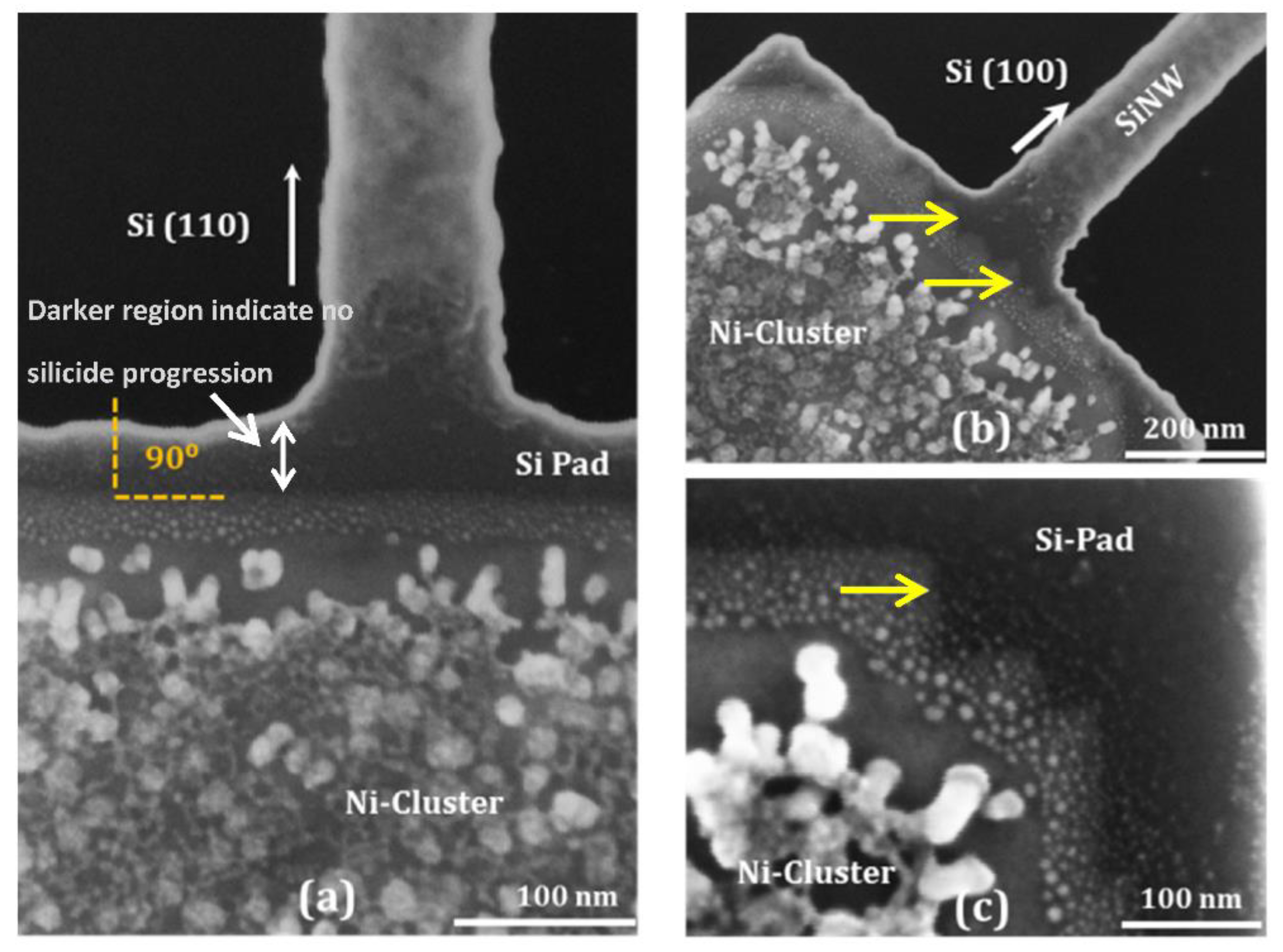
3.1. Silicidation in Si Thin Film Structures
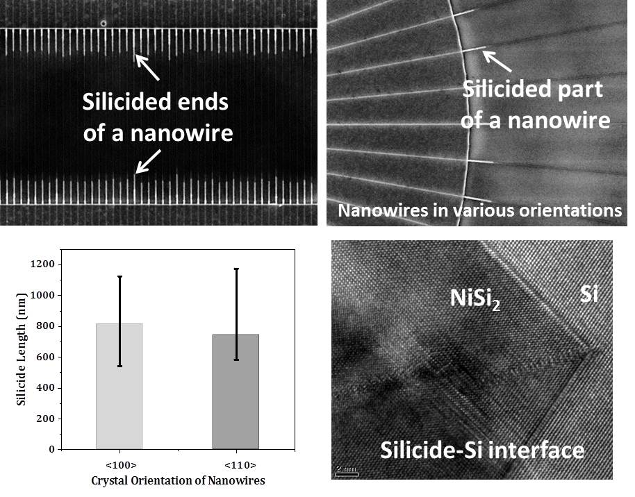
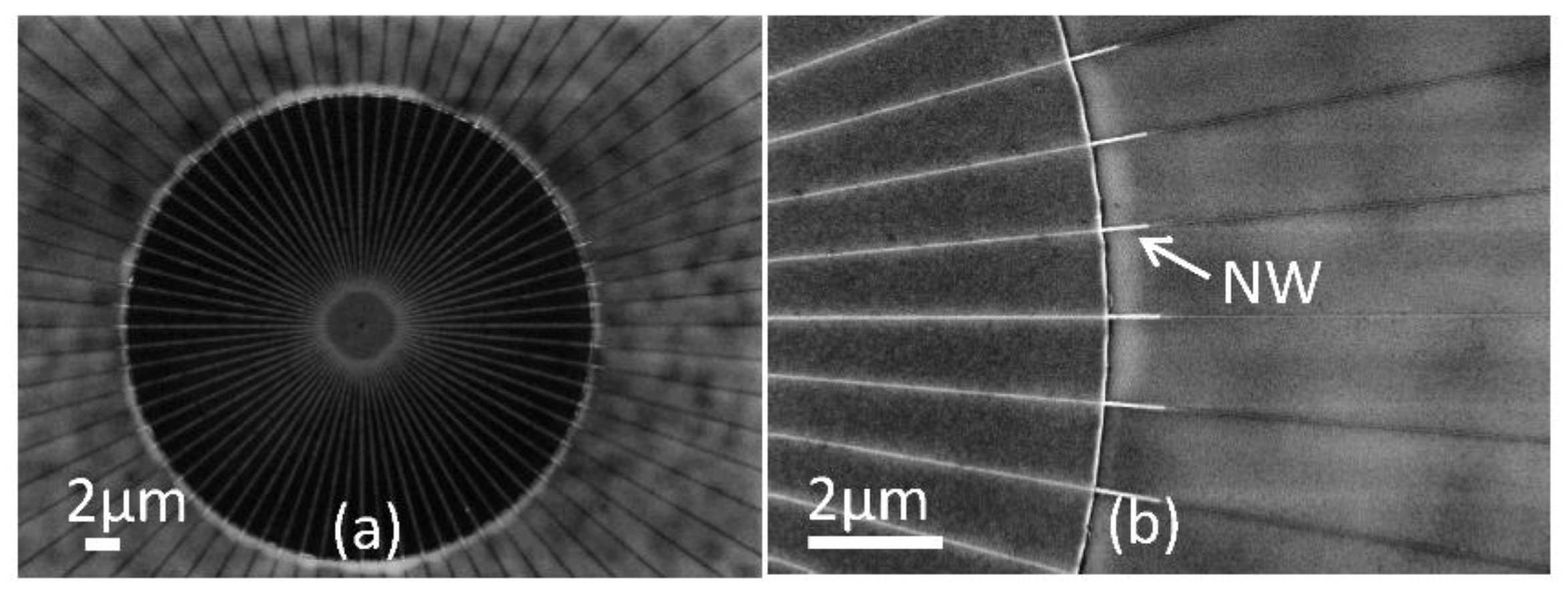
3.2. Silicidation in Nanowires
3.3. Properties of Silicide–Si Interface
3.4. Electrical Characterization of Fabricated Devices
4. Conclusions
Author Contributions
Funding
Acknowledgments
Conflicts of Interest
References
- Yeo, Y.C.; Gong, X.; Van Dal, M.J.H.; Vellianitis, G.; Passlack, M. Germanium-based transistors for future high performance and low power logic applications. In Proceedings of the 2015 IEEE International Electron Devices Meeting (IEDM), Washington, DC, USA, 7–9 December 2015; p. 2. [Google Scholar]
- Dong, R.; Han, P.; Arora, H.; Ballabio, M.; Karakus, M.; Zhang, Z.; Shekhar, C.; Adler, P.; Petkov, P.S.; Erbe, A.; et al. High-mobility band-like charge transport in a semiconducting two-dimensional metal–organic framework. Nat. Mater. 2018, 17, 1027. [Google Scholar] [CrossRef]
- Wang, J.; Yao, Q.; Huang, C.-W.; Zou, X.; Liao, L.; Chen, S.; Fan, Z.; Zhang, K.; Wu, W.; Xiao, X.; et al. High Mobility MoS2 Transistor with Low Schottky Barrier Contact by Using Atomic Thick h-BN as a Tunneling Layer. Adv. Mater. 2016, 28, 8302–8308. [Google Scholar] [CrossRef] [PubMed]
- Chau, R.; Brask, J.; Datta, S.; Dewey, G.; Doczy, M.; Doyle, B.; Kavalieros, J.; Jin, B.; Metz, M.; Majumdar, A.; et al. Application of high-κ gate dielectrics and metal gate electrodes to enable silicon and non-silicon logic nanotechnology. Microelectron. Eng. 2005, 80, 1–6. [Google Scholar] [CrossRef]
- Arabi, K.; Samadi, K.; Du, Y. 3D VLSI: A Scalable Integration beyond 2D. In Proceedings of the 2015 Symposium on International Symposium on Physical Design, Monterey, CA, USA, 29 March–1 April 2015; pp. 1–7. [Google Scholar]
- Das Sarma, S.; Fabian, J.; Hu, X.; Žutić, I. Spin electronics and spin computation. Solid State Commun. 2001, 119, 207–215. [Google Scholar] [CrossRef]
- Risch, L. Pushing CMOS beyond the roadmap. Solid-State Electron. 2006, 50, 527–535. [Google Scholar] [CrossRef]
- Heinzig, A.; Slesazeck, S.; Kreupl, F.; Mikolajick, T.; Weber, W.M. Reconfigurable Silicon Nanowire Transistors. Nano Lett. 2011, 12, 119–124. [Google Scholar] [CrossRef]
- Heinzig, A.; Mikolajick, T.; Trommer, J.; Grimm, D.; Weber, W.M. Dually Active Silicon Nanowire Transistors and Circuits with Equal Electron and Hole Transport. Nano Lett. 2013, 13, 4176–4181. [Google Scholar] [CrossRef]
- Chang, Y.-J.; Erskine, J.L. Diffusion layers and the Schottky-barrier height in nickel silicide—silicon interfaces. Phys. Rev. B 1983, 28, 5766–5773. [Google Scholar] [CrossRef]
- Ottaviani, G.; Tu, K.N.; Mayer, J.W. Barrier heights and silicide formation for Ni, Pd, and Pt on silicon. Phys. Rev. B 1981, 24, 3354–3359. [Google Scholar] [CrossRef]
- Léonard, F.; Talin, A.A. Electrical contacts to one- and two-dimensional nanomaterials. Nat. Nanotechnol. 2011, 6, 773–783. [Google Scholar] [CrossRef]
- Larson, J.; Snyder, J. Overview and status of metal S/D Schottky-barrier MOSFET technology. IEEE Trans. Electron Devices 2006, 53, 1048–1058. [Google Scholar] [CrossRef]
- Simon, M.; Heinzig, A.; Trommer, J.; Baldauf, T.; Mikolajick, T.; Weber, W.M. Top-down technology for reconfigurable nanowire FETs with symmetric on-currents. IEEE Trans. Nanotechnol. 2017, 16, 1. [Google Scholar] [CrossRef]
- Bagdasarov, K.S.; Lube, É.L. Growth of Crystals; Springer: Boston, MA, USA, 1991; Volume 16, p. 278. [Google Scholar]
- Weber, W.M.; Geelhaar, L.; Graham, A.P.; Unger, E.; Duesberg, G.S.; Liebau, M.; Pamler, W.; Cheze, C.; Riechert, H.; Lugli, P.; et al. Silicon-Nanowire Transistors with Intruded Nickel-Silicide Contacts. Nano Lett. 2006, 6, 2660–2666. [Google Scholar] [CrossRef] [PubMed]
- Tang, W.; Dayeh, S.A.; Picraux, S.T.; Huang, J.Y.; Tu, K.-N. Ultrashort Channel Silicon Nanowire Transistors with Nickel Silicide Source/Drain Contacts. Nano Lett. 2012, 12, 3979–3985. [Google Scholar] [CrossRef] [PubMed]
- Tang, W.; Nguyen, B.-M.; Chen, R.; Dayeh, S.A. Solid-state reaction of nickel silicide and germanide contacts to semiconductor nanochannels. Semicond. Sci. Technol. 2014, 29, 054004. [Google Scholar] [CrossRef]
- Beregovsky, M.; Katsman, A.; Hajaj, E.; Yaish, Y. Diffusion formation of nickel silicide contacts in SiNWs. Solid-State Electron. 2013, 80, 110–117. [Google Scholar] [CrossRef]
- Chen, Y.; Huang, Y. Phase control in solid state silicide nanowire formation. Phys. Status Solidi 2013, 10, 1666–1669. [Google Scholar] [CrossRef]
- Yaish, Y.E.; Katsman, A.; Cohen, G.M.; Beregovsky, M. Kinetics of nickel silicide growth in silicon nanowires: From linear to square root growth. J. Appl. Phys. 2011, 109, 94303. [Google Scholar] [CrossRef]
- Ogata, K.; Sutter, E.; Zhu, X.; Hofmann, S. Ni-silicide growth kinetics in Si and Si/SiO2 core/shell nanowires. Nanotechnology 2011, 22, 365305. [Google Scholar] [CrossRef] [PubMed][Green Version]
- Katsman, A.; Beregovsky, M.; Yaish, Y.E. Evolution of nickel silicide intrusions in silicon nanowires during thermal cycling. J. Appl. Phys. 2013, 113, 084305. [Google Scholar] [CrossRef]
- Dellas, N.S.; Abraham, M.; Minassian, S.; Kendrick, C.; Mohney, S.E. Kinetics of reactions of Ni contact pads with Si nanowires. J. Mater. Res. 2011, 26, 2282–2285. [Google Scholar] [CrossRef]
- Lu, K.-C.; Tu, K.N.; Wu, W.W.; Chen, L.J.; Yoo, B.-Y.; Myung, N.V. Point contact reactions between Ni and Si nanowires and reactive epitaxial growth of axial nano-NiSi/Si. Appl. Phys. Lett. 2007, 90, 253111. [Google Scholar] [CrossRef]
- Dellas, N.S.; Liu, B.Z.; Eichfeld, S.M.; Eichfeld, C.M.; Mayer, T.S.; Mohney, S.E. Orientation dependence of nickel silicide formation in contacts to silicon nanowires. J. Appl. Phys. 2009, 105, 94309. [Google Scholar] [CrossRef]
- Dellas, N.S.; Schuh, C.J.; Mohney, S.E. Silicide formation in contacts to Si nanowires. J. Mater. Sci. 2012, 47, 6189–6205. [Google Scholar] [CrossRef]
- Lin, Y.-C.; Chen, Y.; Xu, D.; Huang, Y. Growth of Nickel Silicides in Si and Si/SiOx Core/Shell Nanowires. Nano Lett. 2010, 10, 4721–4726. [Google Scholar] [CrossRef] [PubMed]
- Appenzeller, J.; Knoch, J.; Tutuc, E.; Reuter, M.; Guha, S. Dual-gate silicon nanowire transistors with nickel silicide contacts. In Proceedings of the 2006 International Electron Devices Meeting, San Francisco, CA, USA, 11–13 December 2006. [Google Scholar]
- Katsman, A.; Beregovsky, M.; Yaish, Y.E. Formation and Evolution of Nickel Silicide in Silicon Nanowires. IEEE Trans. Electron Devices 2014, 61, 3363–3371. [Google Scholar] [CrossRef]
- Chou, Y.-C.; Tang, W.; Chiou, C.-J.; Chen, K.; Minor, A.M.; Tu, K.N. Effect of Elastic Strain Fluctuation on Atomic Layer Growth of Epitaxial Silicide in Si Nanowires by Point Contact Reactions. Nano Lett. 2015, 15, 4121–4128. [Google Scholar] [CrossRef] [PubMed]
- Habicht, S.; Zhao, Q.-T.; Feste, S.F.; Knoll, L.; Trellenkamp, S.; Ghyselen, B.; Mantl, S. Electrical characterization of strained and unstrained silicon nanowires with nickel silicide contacts. Nanotechnology 2010, 21, 105701. [Google Scholar] [CrossRef]
- Habicht, S.; Zhao, Q.; Feste, S.; Knoll, L.; Trellenkamp, S.; Bourdelle, K.K.; Mantl, S. NiSi nano-contacts to strained and unstrained silicon nanowires. In Proceedings of the 2011 Materials for Advanced Metallization (MAM), Dresden, Germany, 8–12 May 2011. [Google Scholar]
- Pregl, S.; Weber, W.M.; Nozaki, D.; Kunstmann, J.; Baraban, L.; Opitz, J.; Mikolajick, T.; Cuniberti, G. Parallel arrays of Schottky barrier nanowire field effect transistors: Nanoscopic effects for macroscopic current output. Nano Res. 2013, 6, 381–388. [Google Scholar] [CrossRef]
- D’Heurie, F.M.; Lavoie, C.; Gas, P.; Philibert, J. Reactive Phase Formation: Some Theory and Applications. In Diffusion Processes in Advanced Technological Materials; Springer Science and Business Media LLC: Berlin, Germany, 2005; pp. 283–332. [Google Scholar]
- Laurila, T.; Molarius, J. Reactive Phase Formation in Thin Film Metal/Metal and Metal/Silicon Diffusion Couples. Crit. Rev. Solid State Mater. Sci. 2003, 28, 185–230. [Google Scholar] [CrossRef]
- Ohring, M. Chapter 1-A Review of Materials Science. In Materials Science of Thin Films, 2nd ed.; Academic Press: San Diego, CA, USA, 2002; pp. 1–56. [Google Scholar]
- Tu, K.-N. Silicon and Silicide Nanowires: Applications, Fabrication, and Properties; Pan Stanford Publishing: Redwood City, CA, USA, 2013. [Google Scholar]
- Koyama, M.; Shigemori, N.; Ozawa, K.; Tachi, K.; Kakushima, K.; Nakatsuka, O.; Ohmori, K.; Tsutsui, K.; Nishiyama, A.; Sugii, N.; et al. Si/Ni-Silicide Schottky junctions with atomically flat interfaces using NiSi2 source. In Proceedings of the European Solid-State Device Research Conference (ESSDERC), Helsinki, Finland, 12–16 September 2011; pp. 231–234. [Google Scholar]
- Iwai, H.; Ohguro, T.; Ohmi, S.-I. NiSi salicide technology for scaled CMOS. Microelectron. Eng. 2002, 60, 157–169. [Google Scholar] [CrossRef]
- Baglin, J.; Atwater, H.; Gupta, D.; D’Heurle, F. Radioactive Ni∗ tracer study of the nickel silicide growth mechanism. Thin Solid Films 1982, 93, 255–264. [Google Scholar] [CrossRef]
- Julies, B.A.; Knoesen, D.; Pretorius, R.; Adams, D. A study of the NiSi to NiSi2 transition in the Ni–Si binary system1. Thin Solid Films 1999, 347, 201–207. [Google Scholar] [CrossRef]
- D’Heurle, F. Diffusion in intermetallic compounds with the CaF2 structure: A marker study of the formation of NiSi2 thin films. J. Appl. Phys. 1982, 53, 5678. [Google Scholar] [CrossRef]
- Wu, Y.; Xiang, J.; Yang, C.; Lu, W.; Lieber, C.M. Single-crystal metallic nanowires and metal/semiconductor nanowire heterostructures. Nature 2004, 430, 61–65. [Google Scholar] [CrossRef] [PubMed]
- Schmitt, A.L.; Higgins, J.M.; Szczech, J.R.; Jin, S. Synthesis and applications of metal silicide nanowires. J. Mater. Chem. 2010, 20, 223–235. [Google Scholar] [CrossRef]
- Murarka, S.P. Chapter IV–Formation. In Silicides for Vlsi Applications; Murarka, S.P., Ed.; Academic Press: San Diego, CA, USA, 1983; pp. 99–131. [Google Scholar]
- Lavoie, C.; D’Heurle, F.; Detavernier, C.; Cabral, C. Towards implementation of a nickel silicide process for CMOS technologies. Microelectron. Eng. 2003, 70, 144–157. [Google Scholar] [CrossRef]
- De Marchi, M.; Sacchetto, D.; Frache, S.; Zhang, J.; Gaillardon, P.-E.; Leblebici, Y.; De Micheli, G. Polarity control in double-gate, gate-all-around vertically stacked silicon nanowire FETs. In Proceedings of the 2012 International Electron Devices Meeting, San Francisco, CA, USA, 10–13 December 2012; p. 8. [Google Scholar]
- Chen, Y.; Lin, Y.-C.; Zhong, X.; Cheng, H.-C.; Duan, X.; Huang, Y. Kinetic Manipulation of Silicide Phase Formation in Si Nanowire Templates. Nano Lett. 2013, 13, 3703–3708. [Google Scholar] [CrossRef]
- Yamashita, H.; Kosugiyama, H.; Shikahama, Y.; Hashimoto, S.; Takei, K.; Sun, J.; Matsukawa, T.; Masahara, M.; Watanabe, T. Impact of thermal history of Si nanowire fabrication process on Ni silicidation rate. Jpn. J. Appl. Phys. 2014, 53, 085201. [Google Scholar] [CrossRef]
- Mirza, M.M.; Velha, P.; Docherty, K.E.; Samarelli, A.; Ternent, G.; Zhou, H.; Li, X.; Paul, D.J. Nanofabrication of high aspect ratio (∼50:1) sub-10 nm silicon nanowires using inductively coupled plasma etching. J. Vac. Sci. Technol. B 2012, 30, 6. [Google Scholar] [CrossRef]
- Henschel, W.; Georgiev, Y.M.; Kurz, H. Study of a high contrast process for hydrogen silsesquioxane as a negative tone electron beam resist. J. Vac. Sci. Technol. B 2003, 21, 2018. [Google Scholar] [CrossRef]
- Liu, H.I. Self-limiting oxidation of Si nanowires. J. Vac. Sci. Technol. B 1993, 11, 2532. [Google Scholar] [CrossRef]
- Liu, H.I.; Biegelsen, D.K.; Ponce, F.; Johnson, N.M.; Pease, R.F.W. Self-limiting oxidation for fabricating sub-5 nm silicon nanowires. Appl. Phys. Lett. 1994, 64, 1383–1385. [Google Scholar] [CrossRef]
- Huang, J.; Loeffler, M.; Muehle, U.; Moeller, W.; Mulders, J.; Kwakman, L.; Van Dorp, W.; Zschech, E. Si amorphization by focused ion beam milling: Point defect model with dynamic BCA simulation and experimental validation. Ultramicroscopy 2018, 184, 52–56. [Google Scholar] [CrossRef]
- Reimer, L. Energy-Filtered Transmission Electron Microscopy; Springer: Berlin/Heidelberg, Germany, 1995. [Google Scholar]
- Atomistix ToolKit. 2015. Available online: https://www.synopsys.com/silicon/quantumatk.html (accessed on 16 August 2019).
- Perdew, J.P.; Burke, K.; Ernzerhof, M. Generalized Gradient Approximation Made Simple. Phys. Rev. Lett. 1996, 77, 3865–3868. [Google Scholar] [CrossRef] [PubMed]
- Fuchs, F.; Gemming, S.; Schuster, J. Electron transport through NiSi2–Si contacts and their role in reconfigurable field-effect transistors. J. Phys. Condens. Matter 2019, 31, 355002. [Google Scholar] [CrossRef] [PubMed]


© 2019 by the authors. Licensee MDPI, Basel, Switzerland. This article is an open access article distributed under the terms and conditions of the Creative Commons Attribution (CC BY) license (http://creativecommons.org/licenses/by/4.0/).
Share and Cite
Khan, M.B.; Deb, D.; Kerbusch, J.; Fuchs, F.; Löffler, M.; Banerjee, S.; Mühle, U.; Weber, W.M.; Gemming, S.; Schuster, J.; et al. Towards Reconfigurable Electronics: Silicidation of Top-Down Fabricated Silicon Nanowires. Appl. Sci. 2019, 9, 3462. https://doi.org/10.3390/app9173462
Khan MB, Deb D, Kerbusch J, Fuchs F, Löffler M, Banerjee S, Mühle U, Weber WM, Gemming S, Schuster J, et al. Towards Reconfigurable Electronics: Silicidation of Top-Down Fabricated Silicon Nanowires. Applied Sciences. 2019; 9(17):3462. https://doi.org/10.3390/app9173462
Chicago/Turabian StyleKhan, Muhammad Bilal, Dipjyoti Deb, Jochen Kerbusch, Florian Fuchs, Markus Löffler, Sayanti Banerjee, Uwe Mühle, Walter M. Weber, Sibylle Gemming, Jörg Schuster, and et al. 2019. "Towards Reconfigurable Electronics: Silicidation of Top-Down Fabricated Silicon Nanowires" Applied Sciences 9, no. 17: 3462. https://doi.org/10.3390/app9173462
APA StyleKhan, M. B., Deb, D., Kerbusch, J., Fuchs, F., Löffler, M., Banerjee, S., Mühle, U., Weber, W. M., Gemming, S., Schuster, J., Erbe, A., & Georgiev, Y. M. (2019). Towards Reconfigurable Electronics: Silicidation of Top-Down Fabricated Silicon Nanowires. Applied Sciences, 9(17), 3462. https://doi.org/10.3390/app9173462