High-Speed VCSEL-Based Transceiver for 200 GbE Short-Reach Intra-Datacenter Optical Interconnects

 , , and
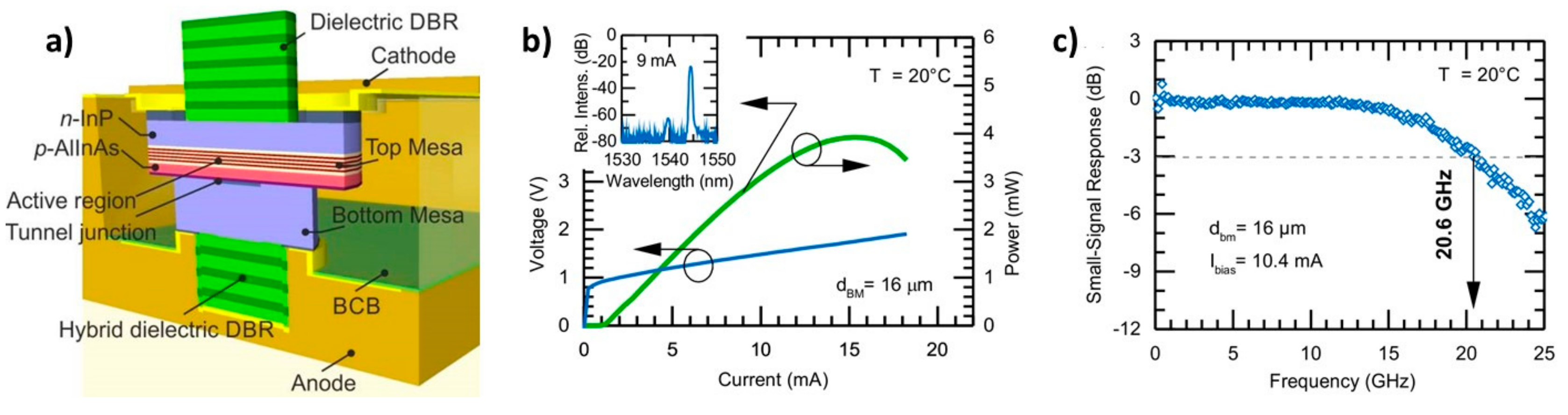
Abstract
:1. Introduction
2. Materials and Methods
2.1. Materials and Architecture of the Devices
2.1.1. High-Speed Single-Mode VCSELs’ Structure and Fabrication Process
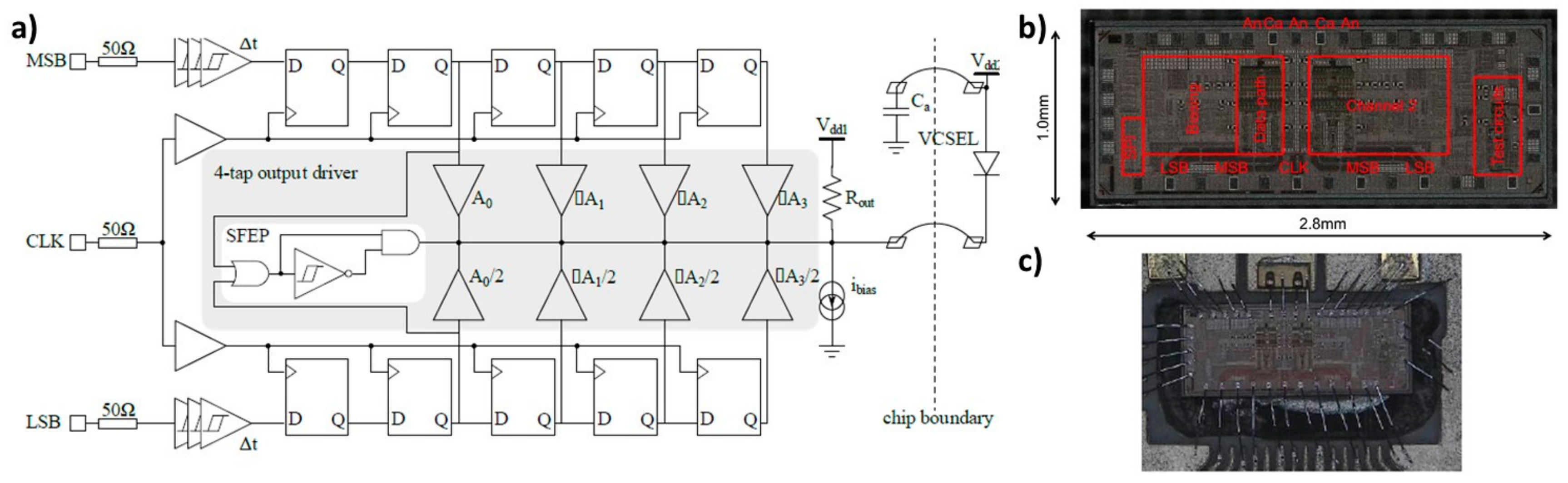
2.1.2. VCSEL-Driver Architecture and Transmitter Assembly
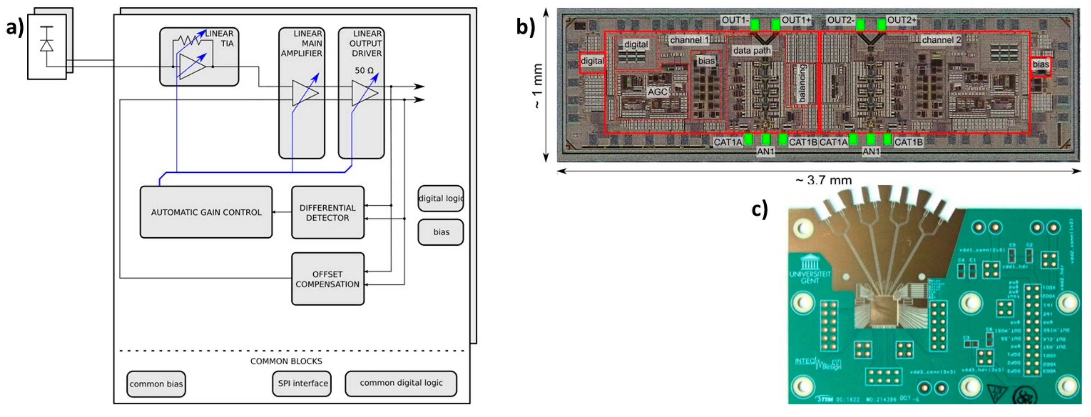
2.1.3. Linear Receiver Architecture and Assembly
2.2. Experimental Setups
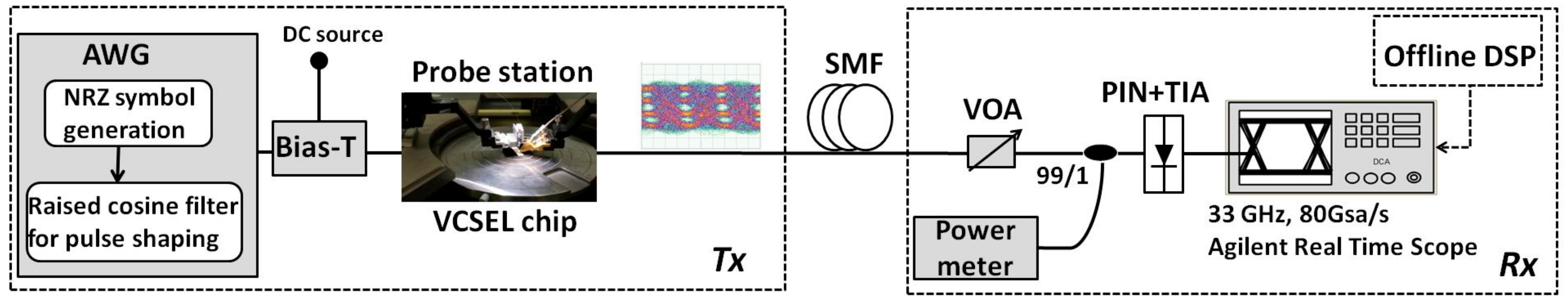
2.2.1. Experimental Setup Used for the Single-Mode High-Speed VCSEL Experiment
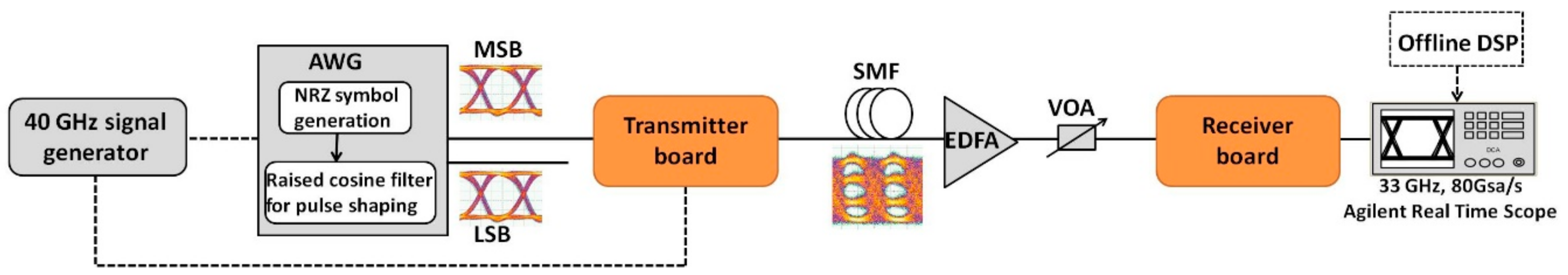
2.2.2. Experimental Setup for the Transceiver Link Experiment
3. Experimental Results and Discussion
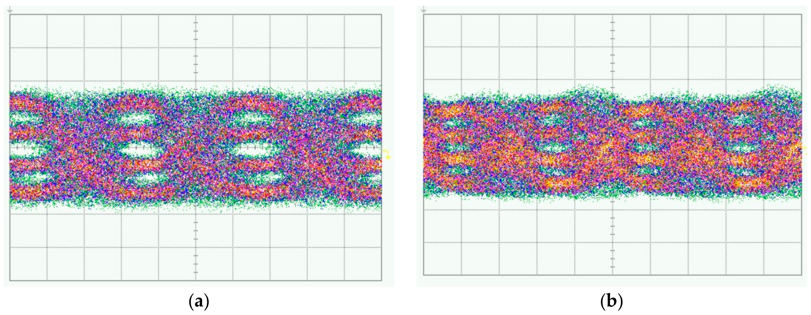
3.1. Transmission of 80 Gb/s up to 500 m Exploiting the High-Speed Single-Mode VCSEL Module
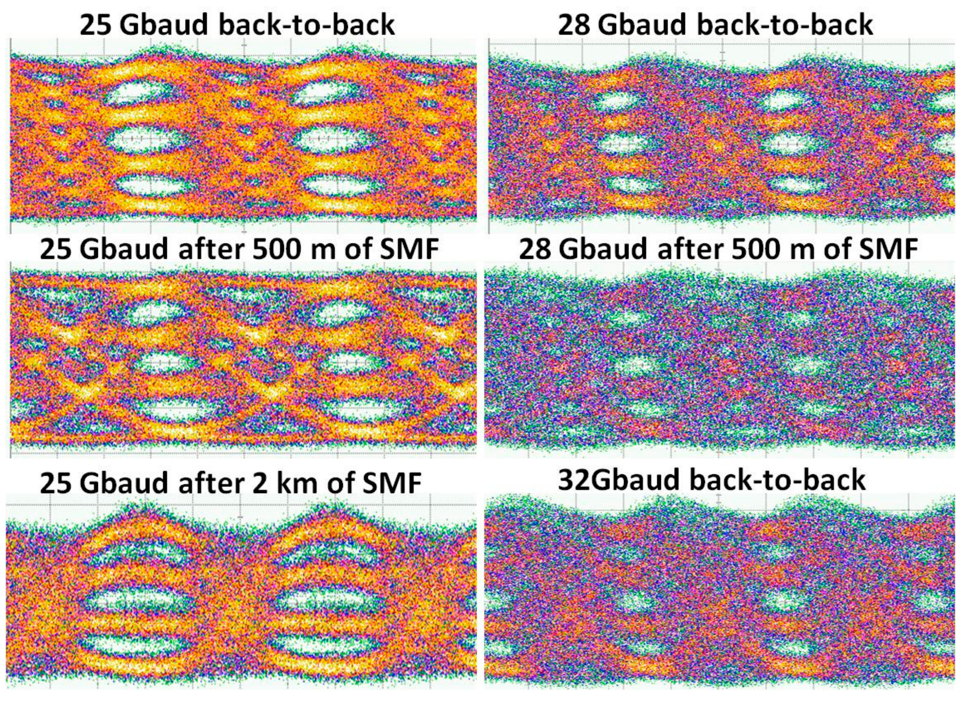
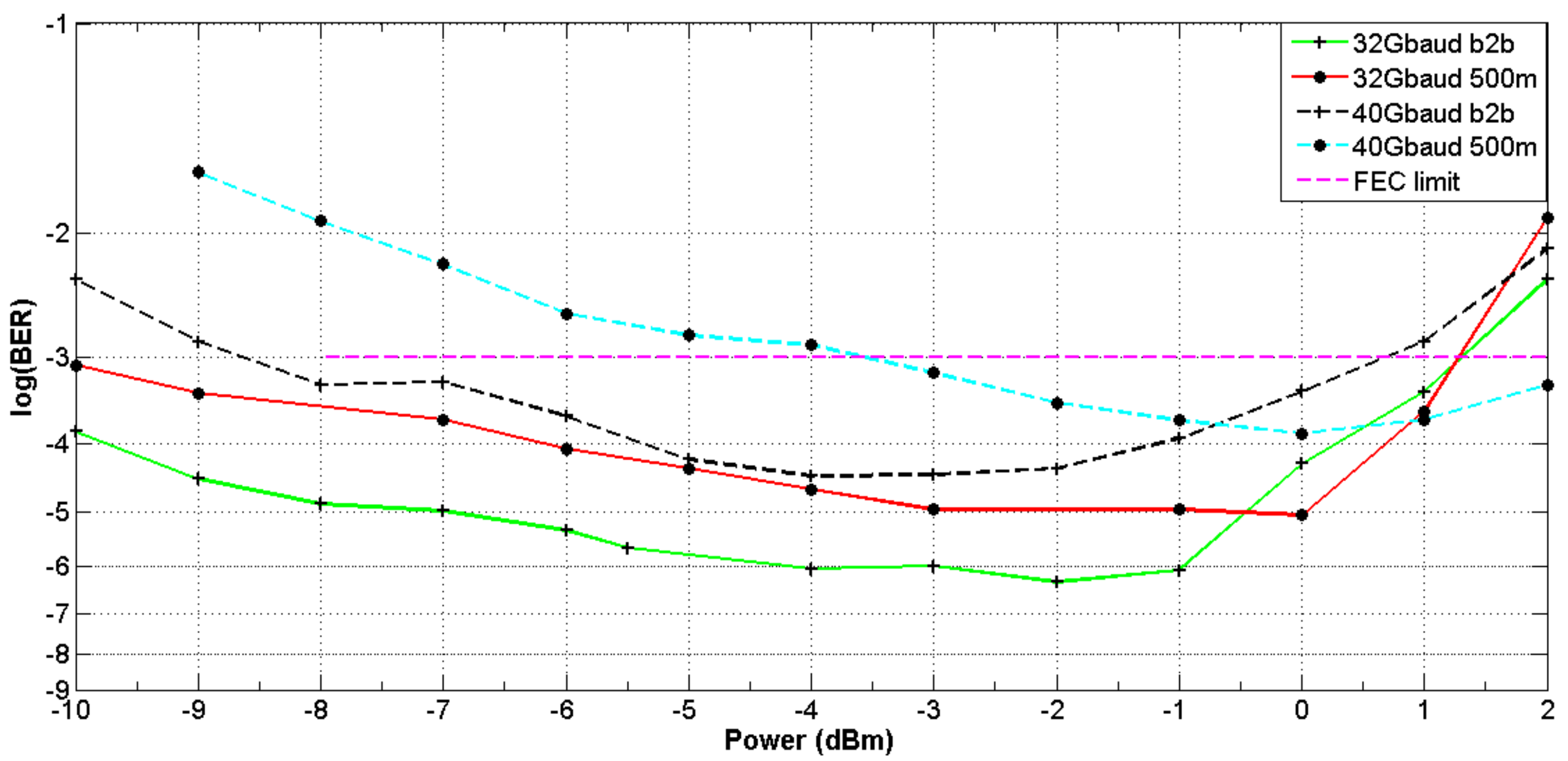
3.2. Up to 64 Gb/s Experiment Employing a VCSEL-Based Transceiver
4. Conclusions
Author Contributions
Funding
Acknowledgments
Conflicts of Interest
References
- Artificial Intelligence and the Impact on Our Data Centers. Available online: https://www.corning.com/emea/en/products/communication-networks/applications/data-center/artificial-intelligence-impact-on-data-centers.html (accessed on 10 April 2019).
- Networking, C.V. Cisco Global Cloud Index: Forecast and Methodology, 2016–2021; White Paper; Cisco Public: San Jose, CA, USA, 2016. [Google Scholar]
- Top 20 Data Center Trends and Predictions to Watch for in 2019. Available online: https://www.upsite.com/blog/top-20-data-center-trends-and-predictions-to-watch-for-in-2019/ (accessed on 10 April 2019).
- Aleksic, S. The future of optical interconnects for data centers: A review of technology trends. In Proceedings of the 2017 14th International Conference on Telecommunications (ConTEL), Zagreb, Croatia, 28–30 June 2017; pp. 41–46. [Google Scholar]
- The Year of 100GbE in Data Center Networks. Available online: https://www.datacenterknowledge.com/networks/year-100gbe-data-center-networks (accessed on 10 April 2019).
- The Race to Higher Speed Optical Transceivers Is Starting to Feel Like a Marathon. Available online: https://www.lightcounting.com/News_100218.cfm (accessed on 10 April 2019).
- New 2018 Ethernet Roadmap Looks to Future Speeds of 1.6 Terabits/s. Available online: https://insidehpc.com/2018/03/new-2018-ethernet-roadmap-looks-future-speeds-1-6-terabits-s/ (accessed on 10 April 2019).
- Lyubomirsky, I.; Ling, W.A. Digital QAM Modulation and Equalization for High Performance 400 GbE Data Center Modules. In Proceedings of the Optical Fiber Communication Conference, San Francisco, CA, USA, 9–13 March 2014. [Google Scholar]
- Iliadis, N.; Kanakis, G.; Spatharakis, C.; Bakopoulos, P.; Avramopoulos, H.; Spiga, S.; Amann, M.-C.; Argyris, N. Optical PAM-4 generation through polarization multiplexing in single-polarization single-mode VCSELs. In Proceedings of the 2016 IEEE International Conference on Electronics, Circuits and Systems (ICECS), Monte Carlo, Monaco, 11–14 December 2016; pp. 360–363. [Google Scholar]
- Kishi, T.; Wakita, H.; Shikama, K.; Nagatani, M.; Kanazawa, S.; Fujii, T.; Nishi, H.; Ishikawa, H.; Kawajiri, Y.; Aratake, A.; et al. A 25-Gbps × 4 ch, Low-Power Compact Wire-Bond-Free 3D-Stacked Transmitter Module with 1.3-μm LD-Array-on-Si for On-Board Optics. In Proceedings of the Optical Fiber Communication Conference (OFC) 2019, San Diego, CA, USA, 3–7 March 2019. [Google Scholar]
- Billah, M.R.; Blaicher, M.; Kemal, J.N.; Hoose, T.; Zwickel, H.; Dietrich, P.I.; Troppenz, U.; Moehrle, M.; Merget, F.; Hofmann, A.; et al. 8-Channel 448 Gbit/s Silicon Photonic Transmitter Enabled by Photonic Wire Bonding. In Proceedings of the Optical Fiber Communication Conference Postdeadline Papers, Los Angeles, CA, USA, 19–23 March 2017. [Google Scholar]
- Denoyer, G.; Chen, A.; Park, B.; Zhou, Y.; Santipo, A.; Russo, R. Hybrid silicon photonic circuits and transceiver for 56 Gb/s NRZ 2.2 km transmission over single mode fiber. In Proceedings of the 2014 The European Conference on Optical Communication (ECOC), Cannes, France, 21–25 September 2014; pp. 1–3. [Google Scholar]
- Dong, P.; Lee, J.; Chen, Y.-K.; Buhl, L.L.; Chandrasekhar, S.; Sinsky, J.H.; Kim, K. Four-Channel 100-Gb/s per Channel Discrete Multitone Modulation Using Silicon Photonic Integrated Circuits. J. Light. Technol. 2016, 34, 79–84. [Google Scholar] [CrossRef]
- Mahgerefteh, D.; Thompson, C.; Cole, C.; DeNoyer, G.; Nguyen, T.; Lyubomirsky, I.; Kocot, C.; Tatum, J. Techno-Economic Comparison of Silicon Photonics and Multimode VCSELs. J. Light. Technol. 2016, 34, 233–242. [Google Scholar] [CrossRef]
- Kuchta, D.M. High Capacity VCSEL-based links. In Proceedings of the Optical Fiber Communication Conference, Los Angeles, CA, USA, 19–23 March 2017. [Google Scholar]
- Lu, I.; Wei, C.-C.; Chen, H.-Y.; Chen, K.-Z.; Huang, C.-H.; Chi, K.-L.; Shi, J.-W.; Lai, F.-I.; Hsieh, D.-H.; Kuo, H.-C.; et al. Very High Bit-Rate Distance Product Using High-Power Single-Mode 850-nm VCSEL with Discrete Multitone Modulation Formats through OM4 Multimode Fiber. IEEE J. Sel. Top. Quantum Electron. 2015, 21, 444–452. [Google Scholar] [CrossRef]
- Kuchta, D.M.; Huynh, T.; Doany, F.; Rylyakov, A.; Schow, C.L.; Pepeljugoski, P.; Gazula, D.; Shaw, E.; Tatum, J. A 4-λ, 40 Gb/s/λ Bandwidth Extension of Multimode Fiber in the 850 nm range. In Proceedings of the Optical Fiber Communication Conference, Los Angeles, CA, USA, 22–26 March 2015. [Google Scholar]
- Haglund, E.; Larsson, A.; Geen, M.; Gustavsson, J.; Haglund, E.; Joel, A.; Westbergh, P.; Haglund, E. 30 GHz bandwidth 850 nm VCSEL with sub-100 fJ/bit energy dissipation at 25–50 Gbit/s. Electron. Lett. 2015, 51, 1096–1098. [Google Scholar] [CrossRef]
- Safaisini, R.; Westbergh, P.; Larsson, A.; Haglund, E.; Gustavsson, J. 20 Gbit/s data transmission over 2 km multimode fibre using 850 nm mode filter VCSEL. Electron. Lett. 2014, 50, 40–42. [Google Scholar] [CrossRef] [Green Version]
- Stepniak, G.; Kropp, J.; Lewandowski, A.; Agustin, M.; Shchukin, V.; Turkiewicz, J.; Schaefer, G.; Ledentsov, N.; Ledentsov, N. 54 Gbit/s OOK transmission using single-mode VCSEL up to 2.2 km MMF. Electron. Lett. 2016, 52, 633–635. [Google Scholar] [CrossRef]
- Kuchta, D.M.; Schow, C.L.; Rylyakov, A.V.; Proesel, J.E.; Doany, F.E.; Baks, C.; Hamel-Bissell, B.H.; Kocot, C.; Graham, L.; Johnson, R.; et al. A 56.1 Gb/s NRZ modulated 850 nm VCSEL-based optical link. In Proceedings of the 2013 Optical Fiber Communication Conference and Exposition and the National Fiber Optic Engineers Conference (OFC/NFOEC), Anaheim, CA, USA, 17–21 March 2013; pp. 1–3. [Google Scholar]
- Castro, J.M.; Pimpinella, R.; Kose, B.; Huang, P.; Lane, B.; Szczerba, K.; Westbergh, P.; Lengyel, T.; Gustavsson, J.S.; Larsson, A.; et al. Investigation of 60 Gb/s 4-PAM Using an 850 nm VCSEL and Multimode Fiber. J. Light. Technol. 2016, 34, 3825–3836. [Google Scholar] [CrossRef]
- Tan, Z.; Yang, C.; Zhu, Y.; Xu, Z.; Zou, K.; Zhang, F.; Wang, Z. A 70 Gbps NRZ optical link based on 850 nm band-limited VCSEL for data-center intra-connects. Sci. China Inf. Sci. 2018, 61, 080406. [Google Scholar] [CrossRef] [Green Version]
- Kuchta, D.M.; Rylyakov, A.V.; Doany, F.E.; Schow, C.L.; Proesel, J.E.; Baks, C.W.; Westbergh, P.; Gustavsson, J.S.; Larsson, A.; Proesel, J. A 71-Gb/s NRZ Modulated 850-nm VCSEL-Based Optical Link. IEEE Photonics Technol. Lett. 2015, 27, 577–580. [Google Scholar] [CrossRef]
- Datacenters to Get a High Fiber Bandwidth Diet. Available online: https://www.nextplatform.com/2016/03/18/datacenters-get-high-fiber-bandwidth-diet/ (accessed on 10 April 2019).
- Malacarne, A.; Sorianello, V.; Daly, A.; Kögel, B.; Ortsiefer, M.; Melo, S.; Neumeyr, C.; Romagnoli, M.; Bogoni, A. High speed long wavelength VCSELs for energy efficient 40 Gbps links up to 1 km without error correction. In Proceedings of the Optical Fiber Communication Conference (OFC), Los Angeles, CA, USA, 22–26 March 2015. [Google Scholar]
- Müller, M.; Wolf, P.; Gründl, T.; Grasse, C.; Rosskopf, J.; Hofmann, W.; Bimberg, D.; Amann, M.-C. Energy efficient 13 μm short cavity VCSELs for 30 Gb/s error-free optical links. In Proceedings of the IEEE International Semiconductor Laser Conference (ISLC), San Diego, CA, USA, 7–10 October 2012. [Google Scholar]
- Kuchta, D.M.; Huynh, T.N.; Doany, F.E.; Schares, L.; Baks, C.W.; Neumeyr, C.; Daly, A.; Kögel, B.; Rosskopf, J.; Ortsiefer, M. Error-free 56 Gb/s NRZ modulation of a 1530 nm VCSEL link. In Proceedings of the European Conference on Optical Communication (ECOC), Valencia, Spain, 27 September–1 October 2015. [Google Scholar]
- Soenen, W.; Vaernewyck, R.; Yin, X.; Spiga, S.; Amann, M.C.; Van Steenberge, G.; Mentovich, E.; Bakopoulos, P.; Bauwelinck, J. 56 Gb/s PAM-4 Driver IC for Long-Wavelength VCSEL Transmitters. In Proceedings of the 42nd European Conference on Optical Communication, Dusseldorf, Germany, 18–22 September 2016; pp. 1–3. [Google Scholar]
- Spiga, S.; Schoke, D.; Andrejew, A.; Boehm, G.; Amann, M. Enhancing the small-signal bandwidth of single-mode 1.5-μm VCSELs. In Proceedings of the 2016 IEEE Optical Interconnects Conference (OI), San Diego, CA, USA, 9–11 May 2016; pp. 14–15. [Google Scholar]
- Collaborative Project ICT-MIRAGE (GA Number 318228); Final Publishable Activity Report, September 2016.
- Moeneclaey, B.; Kanakis, G.; Verbrugghe, J.; Iliadis, N.; Soenen, W.; Kalavrouziotis, D.; Spatharakis, C.; Dris, S.; Yin, X.; Bakopoulos, P.; et al. A 64 Gb/s PAM-4 linear optical receiver. In Proceedings of the 2015 Optical Fiber Communications Conference and Exhibition (OFC), Los Angeles, CA, USA, 22–26 March 2015; pp. 1–3. [Google Scholar]
- Moeneclaey, B.; Verbrugghe, J.; Blache, F.; Goix, M.; Lanteri, D.; Duval, B.; Achouche, M.; Bauwelinck, J.; Yin, X. A 40-Gb/s Transimpedance Amplifier for Optical Links. IEEE Photonics Technol. Lett. 2015, 27, 1375–1378. [Google Scholar] [CrossRef]


© 2019 by the authors. Licensee MDPI, Basel, Switzerland. This article is an open access article distributed under the terms and conditions of the Creative Commons Attribution (CC BY) license (http://creativecommons.org/licenses/by/4.0/).
Share and Cite
Kanakis, G.; Iliadis, N.; Soenen, W.; Moeneclaey, B.; Argyris, N.; Kalavrouziotis, D.; Spiga, S.; Bakopoulos, P.; Avramopoulos, H. High-Speed VCSEL-Based Transceiver for 200 GbE Short-Reach Intra-Datacenter Optical Interconnects. Appl. Sci. 2019, 9, 2488. https://doi.org/10.3390/app9122488
Kanakis G, Iliadis N, Soenen W, Moeneclaey B, Argyris N, Kalavrouziotis D, Spiga S, Bakopoulos P, Avramopoulos H. High-Speed VCSEL-Based Transceiver for 200 GbE Short-Reach Intra-Datacenter Optical Interconnects. Applied Sciences. 2019; 9(12):2488. https://doi.org/10.3390/app9122488
Chicago/Turabian StyleKanakis, Giannis, Nikos Iliadis, Wouter Soenen, Bart Moeneclaey, Nikolaos Argyris, Dimitrios Kalavrouziotis, Silvia Spiga, Paraskevas Bakopoulos, and Hercules Avramopoulos. 2019. "High-Speed VCSEL-Based Transceiver for 200 GbE Short-Reach Intra-Datacenter Optical Interconnects" Applied Sciences 9, no. 12: 2488. https://doi.org/10.3390/app9122488