Article

Crystalline Orientation Identification of Phosphorene Using Polarized Raman Spectroscopy without Analyzer

1
Tianjin Key Laboratory of Modern Engineering Mechanics, School of Mechanical Engineering, Tianjin University, Tianjin 300072, China
2
Tianjin Key Laboratory of High Speed Cutting and Precision Machining, School of Mechanical Engineering, Tianjin University of Technology and Education, Tianjin 300220, China
*
Author to whom correspondence should be addressed.
Co-first author.
Appl. Sci. 2019, 9(11), 2198; https://doi.org/10.3390/app9112198
Submission received: 20 April 2019 / Revised: 17 May 2019 / Accepted: 22 May 2019 / Published: 29 May 2019
(This article belongs to the Section Mechanical Engineering)

Abstract

:

Featured Application

Scientific investigation on interface mechanics of 2-D nanomaterials, Design and manufacture of new semiconductor device based on nano-heterostructure.

Abstract

The unique photoelectric properties of phosphorene typically include anisotropy, hence the nondestructive and rapid identification of its crystal orientation is a key point to the investigation and application of phosphorene. Currently, the orientation identification by analyzing the Ag1 mode based on parallel-polarized Raman has severe requirements for the applicable Raman system. Therefore, it is necessary to develop a more general, convenient, and accurate method for determining the crystal orientation of phosphorene. In this paper, a method of orientation identification was proposed by using a Raman system without an analyzer and quantifying the correlation between the intensities of Ag1 and Ag2 modes with the change of the incident polarization direction. By using mechanically peeled phosphorene as specimens, Raman measurements were carried out under the Raman configurations of both parallel polarization and with no analyzer. The results show that the crystal orientation of phosphorene can be accurately identified by quantifying the Raman intensities of both Ag1 and Ag2 modes using the Raman system without an analyzer.

Graphical Abstract

1. Introduction

Monolayer or few-layer black phosphorus is generally called phosphorene [1], which is a typical two-dimensional (2D) material. Compared with graphene [2], transition-metal sulphides, and other 2D materials [3] phosphorene has unique properties in acoustics [4], optics [5], thermotics [6], electrics [7,8], and mechanics [9,10], which are usually anisotropic, viz. intensively depending on its crystal orientation. These properties, especially owing to their anisotropy, prospectively make phosphorene a kernel material of microelectronic and optoelectronic devices of the new generation [11]. Hence the nondestructive, accurate, and rapid identification of its crystal orientation is a key point to the investigation and application of phosphorene [12].
For the identification of the crystal orientation of phosphorene, the existing methods mainly include microscopic observation based on TEM and AFM, angle-resolution electric conductivity, and spectroscopy methods such as infrared and Raman. Among them, the angle-resolution electric conductivity method is a contact measurement method with low spatial resolution and angle resolution sensitivity [11]. It is difficult to realize an on-line and quantitative measurement using the microscopic observation method. Besides, the spectral resolution and spatial resolution of most infrared spectrometers hardly match the precise requirement of the crystal orientation measurements for phosphorene samples at the micro-scale [7,11].
Because of these characteristics, such as high resolution, high sensitivity, nondestructive, and non-contact measurement [13,14], Raman spectroscopy has been widely applied in experimental investigations on the optical [5] and mechanical [9,15] behaviors of nanomaterials. It has been proved that polarized Raman spectroscopy can be used to identify the crystal orientation of phosphorene rapidly and accurately [11]. The existing studies about crystal-orientation identification using Raman usually adopted the parallel-polarized Raman configuration, in which the polarization directions of the detected scattering light are kept parallel to that of the incident exciting laser. To realize this configuration, the Raman system should be equipped a polarizer in the incident path and an analyzer in the scattering path. Furthermore, both the polarizer and the analyzer, or the sample stage, should be 360° in-situ rotatable with a certain angle step. By fitting the Raman intensities of Ag2 mode in the Raman information of phosphorene under different polarization directions, the crystal orientation can be estimated [11].
However, for most of the micro-Raman systems, neither the 360° rotatable analyzer nor a 360° in-situ rotatable sample stage is a standard accessory. Some published work had to rotate the sample manually, which shows it is difficult to keep the sampling spot in-situ, especially for the cases of complex structures or loading modes. At the same time, because of the inherent and complicated interactions of electron–photon and electron–phonon, laser wavelength and specimen thickness influence the angular dependence of Raman intensity [5,16,17] which may induce an inaccurate or even a mistaken identification of crystal orientation by using the existing methods for the phosphorene sample of multi-layer or under deformation state [5,9,10]. Therefore, it is necessary to develop a more general, convenient, and accurate method for determining the crystal orientation of phosphorene.
In this paper, an identification method of phosphorene orientation was proposed by using a Raman system without analyzer. A 360° continuously rotatable polarizer was used to change the polarization direction of the incident laser. The Raman information was collected at different incident polarization directions without any analyzer. By quantifying the correlation between the polarized angles and the intensities of both Ag1 and Ag2 modes respectively, the crystal orientation of phosphorene can be identified comprehensively.

2. Materials and Methods

2.1. Specimen Preparations

The phosphorene specimens used in this work were obtained as follows. Numbers of phosphorene pieces were mechanically peeled from a block of monocrystalline black phosphorus using 3M Scotch tapes. Then, these pieces on the tapes were transferred onto Si substrates coated with 300 nm SiO2 on the surfaces by mechanically pressing. Some few-layer samples were selected, by using a Zeiss Scope1 optic microscope, as the specimens to be measured.
The layer number of each selected phosphorene specimen was identified according to its Raman spectrum. Quite a few methods were applicable to analyze the layer number of phosphorene, including micro-Raman spectroscopy [18,19], photoluminescence spectroscopy [12], AFM [7], and the optical microscope [20]. In this work, the specimens were observed using an optical microscope [21] to evaluate the layer numbers by contrasting the color. Then, the layer numbers of different sampling spots of the same or different specimens were confirmed by quantifying the distances of the wavenumbers of Ag2 and B2g modes in the Raman spectra of the sampling spots. To save the specimens from oxidation, the identification experiments of both layer numbers and crystal orientations were conducted immediately after specimen preparations.

2.2. Experiment System and Method

The experiments in this work were carried out based on polarized micro-Raman system. Figure 1 shows the optical-path of different polarized micro-Raman system. In detail, Figure 1a gives the optical-path of general polarized micro-Raman system. When the optical axes of both the polarizer and the analyzer in Figure 1a are all 360° continuously adjustable, most of typical polarized configurations of backscattering Raman are realizable. For instance, the parallel-polarized (PP) configuration is realized by keeping the polarized direction of the scattering light paralleling to that of the incident laser.
Figure 1b shows the optical-path of a standard micro-Raman system, which has no analyzer but is equipped with a continuously adjustable polarizer in front of the laser output. Using this system, the polarized direction of the incident laser can be adjusted continuously but that of the scattering light is un-adjustable, which means that the scattering data with all the polarized directions are received and detected by the spectrograph. This polarized configuration is named as the non-analyzer (NA) configuration.
Figure 1c is an upgrade optical-path of micro-Raman system equipped with a continuously adjustable polarizer inside the microscope and an orthogonally switched analyzer inside the spectrograph. The polarizer is a continuously synergistic/co-variant polarized accessory (CS/CV-PA, Chinese patent CN102426163A) and it locates at the overlap path of the incident laser and scattering light. The orthogonally switched analyzer (OSA) is an optional accessory of most of the advanced micro-Raman system such as Renishaw InVia Reflex. When the OSA is switched to parallel, the parallel-polarized configuration is realized and the polarized direction of the scattering light, paralleling to that of the incident laser, is adjusted through the CS/CV-PA. At this time, the system in Figure 1c is similar with that in Figure 1a. When the OSA is switched to gap, the polarized direction of the incident laser can be adjusted continuously by the CS/CV-PA and the scattering data with all the polarized directions are received and detected by the spectrograph, which acts in a similar way to the system in Figure 1b.
The polarized Raman experiments in this work adopted both the non-analyzer and the parallel-polarized configurations by using a Renishaw InVia Reflex confocal micro-Raman spectroscopy system whose optical-path is similar with that in Figure 1c. A Leica 100 × Lens (numerical aperture = 0.85), a 1200 l/mm grating, and a 633 nm laser (1.96 eV) were chosen. The exposure time of each Raman detection was 4 s, and the laser power reached the specimen surface was about 0.64 mW.
During the experiments, the sampling spots were selected using the microscope of the Raman system, the polarized configuration was switched between NA and PP by the OSA, and the polarized direction of the incident laser was rotated from 0° to 360° with a step of 10° by CS/CV-PA. At each sampling spot, the Raman spectra were detected in situ at different polarized directions of the incident laser under both NA and PP configuration. The Raman intensities of both Ag1 and Ag2 modes were obtained by fitting the spectra using a pseudo-Voigt function.

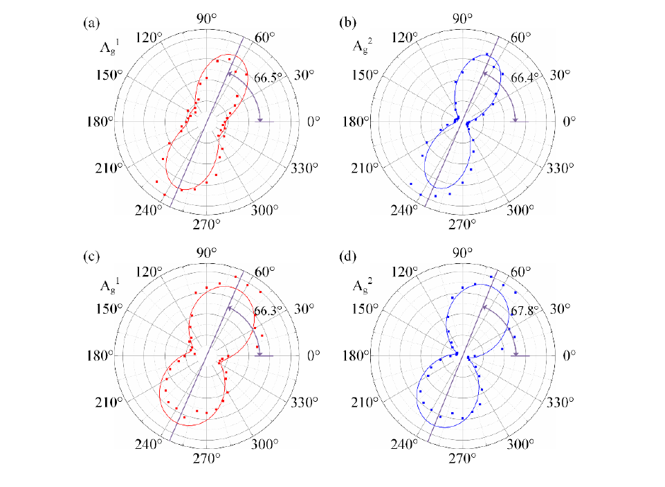
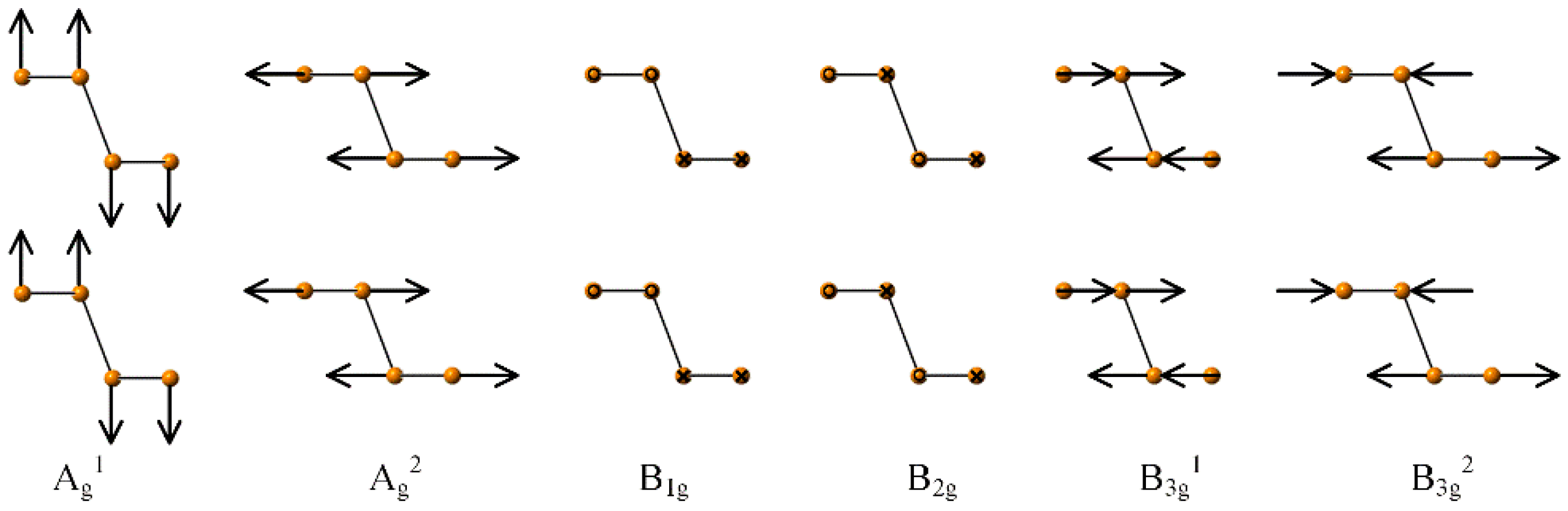
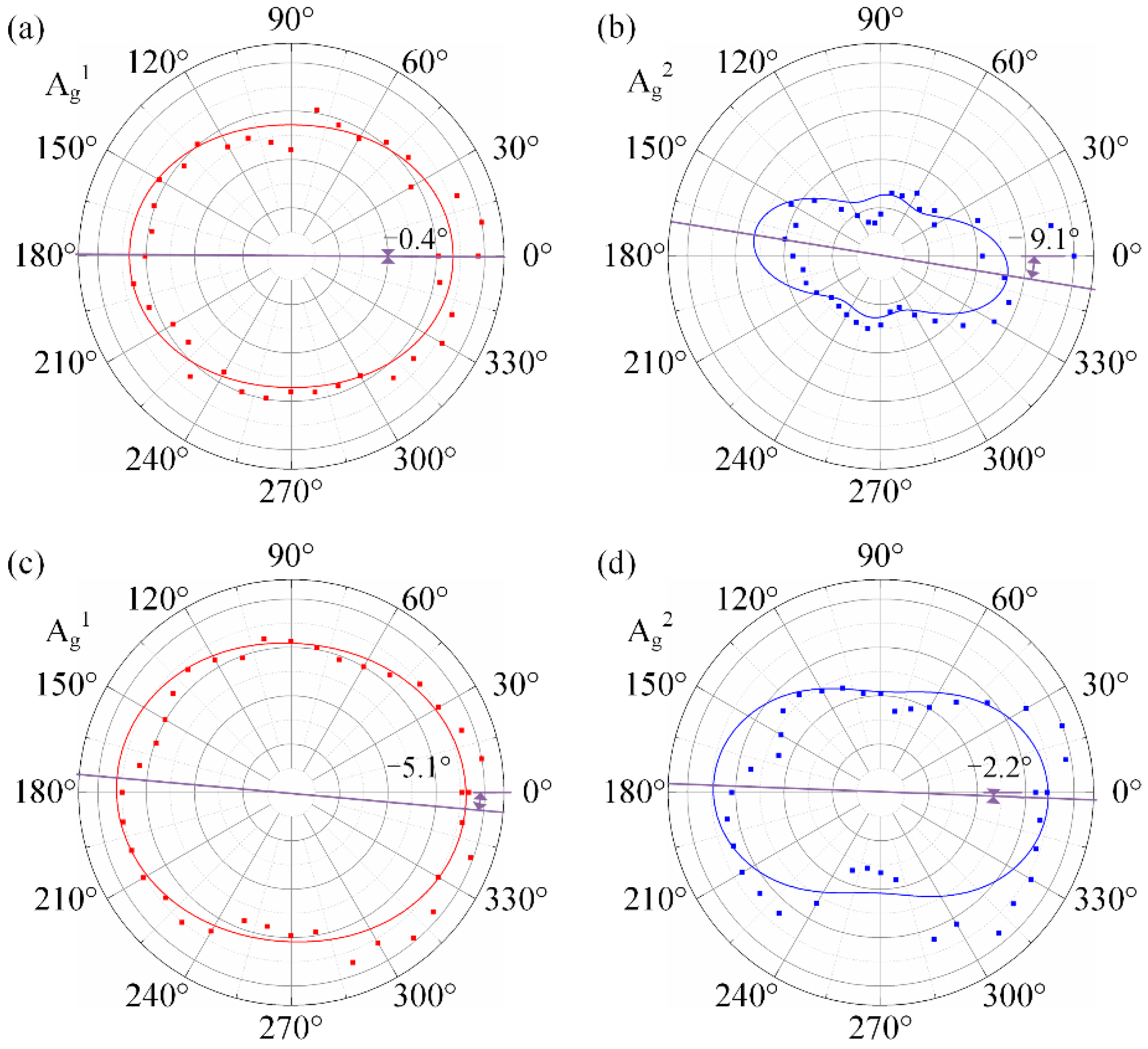
3. Results and Discussion

Figure 2 shows the crystalline structure of phosphorene. Table 1 gives the Raman tensors for all active modes of phosphorene, whose corresponding atomic displacements are displayed in Figure 3. It can be seen that phosphorene has six Raman-active vibration modes. In backscattering geometry configuration, only Ag (including Ag1 and Ag2) and B2g mode are Raman visible [22] where Ag1, Ag2, and B2g correspond to the atomic vibrations along the out-of-plane direction, armchair (AC) direction, and zigzag (ZZ) direction, respectively.
Figure 4a shows the optical image of phosphorene specimens, where the cross point in the dashed box is the Raman sampling spot at that time, X and Y are the horizontal and vertical directions of the sample stage of the Raman system, φ is the angle from the polarized direction of the incident light to the X-axis and θ is the angle from the armchair direction of the phosphorene specimen to the X-axis, which is the crystalline orientation to be identified in this work. Figure 4b shows the Raman spectra of a phosphorene specimen when φ was 180°, where the positions of Ag1, B2g, and Ag2 modes correspond to ~363 cm−1, ~440 cm−1, and ~470 cm−1, respectively. The distance between the Ag2 and B2g mode is about 28.8 cm−1, then the measured specimen was a 3-layer phosphorene [20].
With the polarized direction of incident laser varying from 0° to 360°, the Raman intensities of phosphorene specimens within 300–500 cm−1 under PP and NA configurations were achieved, shown in the Figure 4c,d, respectively. The angular-spectral images show that the intensity of each mode changes with the polarization direction obviously. Based on the results in the Figure 4c,d, the fitted and then normalized data of Ag1 and Ag2 intensities are listed in the polar coordinates as shown in the Figure 5, where each solid square point corresponds to the experimental datum whose distance to the center of the polar coordinates denotes its normalized Raman intensity and angular position denotes the polarized direction of incident laser (viz. φ). In Figure 5a,b show the data under PP configuration, and Figure 5c,d, the data under NA configuration.
Figure 5 reveals the angular dependence of the Raman intensities of both the Ag1 and Ag2 modes, which can be described theoretically. According to the Raman tensors in Table 1 and the Raman selecting rules, the Raman intensity of each mode is given by Equation (1) [22].
I s | e i R e s T | 2
Existing studies discovered that the Raman scattering intensity of phosphorene was influenced by the light absorption. Hence the Raman tensors of phosphorene, listed in Table 1, should be represented as the forms of complex function as Equation (2) [5,22].
a = | a | e i ϕ a , b = | b | e i ϕ b , c = | c | e i ϕ c
And the phases of Raman tensor elements a, b, c are
ϕ a = arctan [ ε xx q A g ε xx q A g ] , ϕ b = arctan [ ε yy q A g ε yy q A g ] , ϕ c = arctan [ ε zz q A g ε zz q A g ]
where ε′i and ε″i (i = x, y, z) are the real part and imaginary part of dielectric function along different crystal direction, εi = ε′ii + iε″ii, and qAg is the normal coordinate of Ag Raman mode.
According to Figure 4a, the polarization vectors of incident laser and scattering light under PP configuration are ei = es = [sin (φθ), cos (φθ)], thus the Raman intensity of Ag mode at PP is as follows.
I A g = [ | a | sin 2 ( φ θ ) + | c | cos ϕ ca cos 2 ( φ θ ) ] 2 + | c | 2 sin 2 ϕ ca cos 4 ( φ θ )
Similarly, when the polarization directions of incident laser and scattering light are keeping perpendicular to each other, the polarization vectors of incident laser and scattering light under orthogonal-polarized (OP) configuration are ei = [sin (φθ), cos (φθ)] and es = [cos (φθ), −sin (φθ)], respectively. The Raman intensity of Ag mode at OP is expressed as Equation (5).
I A g = [ ( | a | | c | cos ϕ ca ) 2 + | c | 2 sin 2 ϕ ca ] sin 2 ( φ θ ) cos 2 ( φ θ )
where φca = φcφa is the phase difference between the complex Raman tensor elements c and a.
The Raman intensity under the NA configuration, IAg, is the sum of those under the parallel-polarized and vertical-polarized configurations [23]. Hence the angular-intensity function for the NA configuration is the superposition of the functions for the PP and OP configurations [24,25,26].
I A g = a 2 sin 2 ( φ θ ) + c 2 cos 2 ( φ θ )
The experimental data in Figure 5a,b were fitted by using Equation (4) and those in Figure 5c,d were fitted by using Equation (6). The fitted curves of Ag1 and Ag2 modes are given in Figure 5 using red and blue lines, respectively. The fitted results of θ in Figure 5 are 66.5° (Ag1 at PP), 66.4° (Ag2 at PP), 66.3° (Ag1 at NA), and 67.8° (Ag2 at NA), respectively. It shows that the identification method of phosphorene crystalline orientation based on a non-analyzer Raman system achieved similar results with those using the traditional method. The deviations between the results of the two methods are much less than the rotating step (10°) of polarized direction during the Raman experiments, which were probably caused by manual rotation of polarizer, curve fitting process and other factors. Hence the Ag1 and Ag2 modes in NA configuration can be used to identify the phosphorene crystalline orientation.
Figure 6, Figure 7, Figure 8 and Figure 9 give the normalized Raman intensities of four different phosphorene specimens of 3, 2, 4, and ~37 (~20 nm by AFM) layers, respectively. All the solid square points denote experimental data, and the solid lines are the fitted curves by using Equation (4) for PP results and Equation (6) for NA results, respectively. These experimental data and fitting results show that the crystalline orientations identified using NA configuration are all similar to those using traditional PP configuration. In detail, the crystalline orientations identified using PP configuration in Figure 6, Figure 7, Figure 8 and Figure 9 are −75.2°, −9.1°, −43.6°, and 96.5°. If using the average values of Ag1 and Ag2 at NA, the crystalline orientations identified using NA configuration in Figure 6, Figure 7, Figure 8 and Figure 9 are −66.9°, −3.7°, −40.7°, and 97.1°. The largest difference between the results of PP and those of NA is 8.3°, less than the rotating step (10°) of polarized direction during the Raman experiments. There results verified the validity and effectiveness of proposed method.
In either the Figure 7b or the Figure 9b, the experimental data of Ag2 showed a secondary maximum at the direction vertical to that of the primary maximum. Moreover, the primary maximum was much larger than the secondary one. Quite a few existing experiments, not only in this work but also some by other groups, detected such a phenomenon similar to that in the Figure 7b or the Figure 9b, which showed this phenomenon of Ag2 might, probably but not inevitably, appear under PP configuration only [17,22]. Mao et al. believed that it was induced by the birefringence relatively obvious under the PP configuration and could be well described by using the Equation (4) [17]. While under the NA configuration, according to the Equation (6) the polarization-intensity curve seemed to be a peanut-like shape with only one maximum direction.
In this work, the layer numbers of all the samples were identified by using the method similar to that in [20] The B2g − Ag2 wavenumber difference, Δω, under NA configuration was used to conclude the layer number by using the following identifying criterion: 1 layer if Δω ≥ 30.3 cm−1, 2 layers if 30.3 cm−1 > Δω ≥ 29.3 cm−1, 3 layers if 29.3 cm−1 > Δω ≥ 28.4 cm−1, 4 layers if 28.4 cm−1 > Δω ≥ 27.8 cm−1, and > 4 layers if 27.8 cm−1 > Δω, where each Δω was the average value of all the 37 data at polarization direction from 0° to 360° with 10° rotating step. As for the samples corresponding to Figure 5, Figure 6, Figure 7, Figure 8 and Figure 9, the Δω were 28.83 cm−1, 29.22 cm−1, 30.09 cm−1, 28.29 cm−1, and 27.59 cm−1, respectively. Hence the layer numbers were regarded as 3, 3, 2, 4, and >4 layers.
In fact, the wavenumber difference Δω used for identifying the layer number clearly depended on whether the PP or NA Raman configurations were used. If using the same identifying criterion on the data under different polarized Raman configurations, the results may be inconsistent. Hence the accurate identification of layer number requires an in-situ measurement combining polarized micro-Raman with AFM.
Besides, the method in this work is more flexible to apply than the traditional one. In detail, as a necessary for PP configuration, the 360° continuously adjustable analyzer is not a standard, but a customized accessory for most of the Raman system and microscope. And it is located inside the cabinet of the spectrograph, which is far from practically for angular-resolution polarized Raman measurement like the identification of the crystalline orientation. The NA configuration, by contrast, is only based on a standard Raman system and only a continuously adjustable polarizer is required. The polarizer can be a general accessory of any optic system, located at any readily accessible place in the incident optic-path such as in front of the laser output, and even be replaced by a 360° continuously adjustable sample stage.
In addition, the NA can also be used to identify crystalline orientation of other anisotropic two-dimensional materials with Raman activity [27]. For example, the Raman intensity of ReS2 at 211 cm−1 shows periodic variation with specimen rotation and reaches its maximum when the crystalline orientation of the ReS2 specimen paralleling to the polarized direction of the incident laser at NA configuration [28], and so do the Raman intensities of WTe2 at 164 cm−1 [29]. Layered b-AsP and GeS [30,31] also have the orthorhombic structure similar to black phosphorus. Existing Raman experiments using NA configuration showed that the Raman intensities of Ag and B2g modes for b-AsP periodically variated with Armchair-polarization angle. Moreover, the Ag1 and Ag2 intensities of GeS showed periodic variation at PP configuration. Due to the crystal structure of GeS similar to that of black phosphorus, it is reasonable to determine the crystal orientation of GeS according to the Raman intensity to polarization angle relationship of Ag1 and Ag2 modes at NA configuration. In sum, the proposed method in this work is also applicable to identify crystalline orientations of ReS2, WTe2, b-AsP, GeS, etc.

4. Conclusions

This work proposed a new method for identifying the crystal orientation of phosphorene based on the micro-Raman system without analyzer. The identification was realized by comprehensively analyzing the intensity changes of the Ag1 and Ag2 Raman modes by collecting the Raman spectra of phosphorene specimens under different polarization directions of incident laser. The comparing experiments were carried out on the same phosphorene specimens under both the parallel-polarized and the non-analyzer configurations, respectively, to verify the effectiveness of the proposed method. The results of the two methods showed good consistence, which proved that the proposed method can accurately identify the crystal orientation of the phosphorene by using a non-analyzer configuration and quantifying the variation of the Raman intensity of Ag1 and Ag2 modes. In contrast to the method using the parallel-polarized configuration, which must be equipped a continuously rotatable polarizer and analyzer or in-situ sample stage, the non-analyzer method has low requirements of the Raman instrument and can be realized more easily. The proposed method can identify the crystalline orientation conveniently and efficiently with a wide range of applications.

Author Contributions

H.-Q.B. and R.-B.L., co-first authors; conceptualization, R.-B.L.; methodology, H.-Q.B.; validation, H.-Q.B.; resources, R.-B.L. and Q.L.; data curation, C.Q.; writing—original draft preparation, H.-D.X.; writing—review and editing, W.Q.

Funding

This research was funded by the national key research and development program of china, grant number 2018yfb0703500 and the national natural science foundation of china, grant numbers 11827802, 11772223 and 11772227, and the natural science foundation of tianjin, grant number 16jcybjc40500.

Acknowledgments

We thank Dawei Li from the University of Nebraska-Lincoln for improvement suggests and comments.

Conflicts of Interest

The authors declare no conflict of interest.

References

  1. Li, L.; Yu, Y.; Ye, G.J.; Ge, Q.; Ou, X.; Wu, H.; Feng, D.; Chen, X.H.; Zhang, Y. Black phosphorus field-effect transistors. Nat. Nanotechnol. 2014, 9, 372–377. [Google Scholar] [CrossRef] [PubMed] [Green Version]
  2. Geim, A.K.; Novoselov, K.S. The rise of graphene. Nat. Mater. 2007, 6, 183–191. [Google Scholar] [CrossRef] [PubMed]
  3. Wang, Q.H.; Kalantar-Zadeh, K.; Kis, A.; Coleman, J.N.; Strano, M.S. Electronics and optoelectronics of two-dimensional transition metal dichalcogenides. Nat. Nanotechnol. 2012, 7, 699–712. [Google Scholar] [CrossRef]
  4. Drissi, L.B.; Sadki, S.; Sadki, K. Phosphorene under strain:electronic, mechanical and piezoelectric responses. J. Phys. Chem. Solids 2018, 112, 137–142. [Google Scholar] [CrossRef]
  5. Ling, X.; Huang, S.; Hasdeo, E.H.; Liang, L.; Parkin, W.M.; Tatsumi, Y.; Nugraha, A.R.T.; Puretzky, A.A.; Das, P.M.; Sumpter, B.G.; et al. Anisotropic electron-photon and electron-phonon interactions in black phosphorus. Nano Lett. 2016, 16, 2260–2267. [Google Scholar] [CrossRef] [PubMed]
  6. Fei, R.; Faghaninia, A.; Soklaski, R.; Yan, J.-A.; Lo, C.; Yang, L. Enhanced Thermoelectric Efficiency via Orthogonal Electrical and Thermal Conductances in Phosphorene. Nano Lett. 2014, 14, 6393–6399. [Google Scholar] [CrossRef] [PubMed] [Green Version]
  7. Xia, F.; Wang, H.; Jia, Y. Rediscovering black phosphorus as an anisotropic layered material for optoelectronics and electronics. Nat. Commun. 2014, 5, 4458. [Google Scholar] [CrossRef] [Green Version]
  8. Fei, R.; Yang, L. Strain-engineering the anisotropic electrical conductance of few-layer black phosphorus. Nano Lett. 2014, 14, 2884–2889. [Google Scholar] [CrossRef]
  9. Li, Y.; Hu, Z.; Lin, S.; Lai, S.K.; Ji, W.; Lau, S.P. Giant Anisotropic Raman Response of Encapsulated Ultrathin Black Phosphorus by Uniaxial Strain. Adv. Funct. Mater. 2017, 27, 1600986. [Google Scholar] [CrossRef]
  10. Wang, Y.; Cong, C.; Fei, R.; Yang, W.; Chen, Y.; Cao, B.; Yang, L.; Yu, T. Remarkable anisotropic phonon response in uniaxially strained few-layer black phosphorus. Nano Res. 2015, 8, 3944–3953. [Google Scholar] [CrossRef]
  11. Wu, J.; Mao, N.; Xie, L.; Xu, H.; Zhang, J. Identifying the crystalline orientation of black phosphorus using angle-resolved polarized Raman spectroscopy. Angew. Chem. Int. Ed. Eng. 2015, 54, 2366–2369. [Google Scholar] [CrossRef]
  12. Li, L.; Kim, J.; Jin, C.; Ye, G.J.; Qiu, D.Y.; da Jornada, F.H.; Shi, Z.; Chen, L.; Zhang, Z.; Yang, F.; et al. Direct observation of the layer-dependent electronic structure in phosphorene. Nat. Nanotechnol. 2017, 12, 21–25. [Google Scholar] [CrossRef]
  13. Kang, Y.; Qiu, Y.; Lei, Z.; Hu, M. An application of Raman spectroscopy on the measurement of residual stress in porous silicon. Opt. Lasers Eng. 2005, 43, 847–855. [Google Scholar] [CrossRef]
  14. Cen, H.; Kang, Y.; Lei, Z.; Qin, Q.; Qiu, W. Micromechanics analysis of Kevlar-29 aramid fiber and epoxy resin microdroplet composite by Micro-Raman spectroscopy. Compos. Struct. 2006, 75, 532–538. [Google Scholar] [CrossRef]
  15. Qiu, W.; Li, Q.; Lei, Z.-K.; Qin, Q.-H.; Deng, W.-L.; Kang, Y.-L. The use of a carbon nanotube sensor for measuring strain by micro-Raman spectroscopy. Carbon 2013, 53, 161–168. [Google Scholar] [CrossRef]
  16. Kim, J.; Lee, J.U.; Lee, J.; Park, H.J.; Lee, Z.; Lee, C.; Cheong, H. Anomalous polarization dependence of Raman scattering and crystallographic orientation of black phosphorus. Nanoscale 2015, 7, 18708–18715. [Google Scholar] [CrossRef] [PubMed] [Green Version]
  17. Mao, N.; Wu, J.; Han, B.; Lin, J.; Tong, L.; Zhang, J. Birefringence-Directed Raman Selection Rules in 2D Black Phosphorus Crystals. Small 2016, 12, 2627–2633. [Google Scholar] [CrossRef]
  18. Wang, X.; Jones, A.M.; Seyler, K.L.; Tran, V.; Jia, Y.; Zhao, H.; Wang, H.; Yang, L.; Xu, X.; Xia, F. Highly anisotropic and robust excitons in monolayer black phosphorus. Nat. Nanotechnol. 2015, 10, 517–521. [Google Scholar] [CrossRef] [Green Version]
  19. Favron, A.; Gaufres, E.; Fossard, F.; Phaneuf-L’Heureux, A.L.; Tang, N.Y.; Levesque, P.L.; Loiseau, A.; Leonelli, R.; Francoeur, S.; Martel, R. Photooxidation and quantum confinement effects in exfoliated black phosphorus. Nat. Mater. 2015, 14, 826–832. [Google Scholar] [CrossRef]
  20. Lu, W.; Nan, H.; Hong, J.; Chen, Y.; Zhu, C.; Liang, Z.; Ma, X.; Ni, Z.; Jin, C.; Zhang, Z. Plasma-assisted fabrication of monolayer phosphorene and its Raman characterization. Nano Res. 2014, 7, 853–859. [Google Scholar] [CrossRef] [Green Version]
  21. Chen, H.; Fei, W.; Zhou, J.; Miao, C.; Guo, W. Layer Identification of Colorful Black Phosphorus. Small 2017, 13, 1602336. [Google Scholar] [CrossRef] [PubMed]
  22. Ribeiro, H.B.; Pimenta, M.A.; de Matos, C.J.S.; Moreira, R.L.; Rodin, A.S.; Zapata, J.D.; de Souza, E.A.T.; Castro Neto, A.H. Unusual Angular Dependence of the Raman Response in Black Phosphorus. ACS Nano 2015, 9, 4270–4276. [Google Scholar] [CrossRef] [PubMed]
  23. Wolverson, D.; Crampin, S.; Kazemi, A.S.; Ilie, A.; Bending, S.J. Raman Spectra of Monolayer, Few-Layer, and Bulk ReSe2: An Anisotropic Layered Semiconductor. ACS Nano 2014, 8, 11154–11164. [Google Scholar] [CrossRef] [PubMed] [Green Version]
  24. Lin, H.C.; Feng, Z.C.; Chen, M.S.; Shen, Z.X.; Ferguson, I.T.; Lu, W. Raman scattering study on anisotropic property of wurtzite GaN. J. Appl. Phys. 2009, 105, 036102. [Google Scholar] [CrossRef]
  25. Saito, R.; Tatsumi, Y.; Huang, S.; Ling, X.; Dresselhaus, M.S. Raman spectroscopy of transition metal dichalcogenides. J. Phys. Condens. Matter 2016, 28, 353002. [Google Scholar] [CrossRef] [PubMed]
  26. Zheng, W.; Zheng, R.S.; Wu, H.L.; Li, F.D. Strongly anisotropic behavior of A1(TO) phonon mode in bulk AlN. J. Alloy. Compd. 2014, 584, 374–376. [Google Scholar] [CrossRef]
  27. Wang, J.; Luo, X.; Li, S.; Verzhbitskiy, I.; Zhao, W.; Wang, S.; Quek, S.Y.; Eda, G. Determination of Crystal Axes in Semimetallic T′-MoTe2 by Polarized Raman Spectroscopy. Adv. Funct. Mater. 2017, 27, 1604799. [Google Scholar] [CrossRef]
  28. Chenet, D.A.; Aslan, O.B.; Huang, P.Y.; Fan, C.; van der Zande, A.M.; Heinz, T.F.; Hone, J.C. In-Plane Anisotropy in Mono- and Few-Layer ReS2 Probed by Raman Spectroscopy and Scanning Transmission Electron Microscopy. Nano Lett. 2015, 15, 5667–5672. [Google Scholar] [CrossRef]
  29. Song, Q.; Pan, X.; Wang, H.; Zhang, K.; Tan, Q.; Li, P.; Wan, Y.; Wang, Y.; Xu, X.; Lin, M.; et al. The in-plane anisotropy of wte2 investigated by angle-dependent and polarized Raman spectroscopy. Sci. Rep. 2016, 6, 29254. [Google Scholar] [CrossRef]
  30. Liu, B.; Köpf, M.; Abbas, A.N.; Wang, X.; Guo, Q.; Jia, Y.; Xia, F.; Weihrich, R.; Bachhuber, F.; Pielnhofer, F.; et al. Black Arsenic–Phosphorus: Layered Anisotropic Infrared Semiconductors with Highly Tunable Compositions and Properties. Adv. Mater. 2015, 27, 4423–4429. [Google Scholar] [CrossRef]
  31. Tan, D.; Lim, H.E.; Wang, F.; Mohamed, N.B.; Mouri, S.; Zhang, W.; Miyauchi, Y.; Ohfuchi, M.; Matsuda, K. Anisotropic optical and electronic properties of two-dimensional layered germanium sulfide. Nano Res. 2017, 10, 546–555. [Google Scholar] [CrossRef]
Figure 1. Optical-path of (a) general polarized micro-Raman system, (b) standard micro-Raman system (without analyzer) equipped with a continuously adjustable polarizer, (c) standard micro-Raman system equipped with a continuously adjustable polarizer and an orthogonally switched analyzer.
Applsci 09 02198 g001
Figure 2. Crystalline structure of Phosphorene. (a) Perspective view, (b) front view, (c) side view, (d) top view.
Applsci 09 02198 g002
Figure 3. Atomic displacements of the Raman-active modes in black phosphorus.
Applsci 09 02198 g003
Figure 4. (a) Optical image of phosphorene specimens, (b) Raman spectra of 3-layer phosphorene specimen under parallel-polarized (PP) and non-analyzer (NA) configurations, respectively, (c,d) angular-spectral images of 3-layer phosphorene specimen under PP and NA configurations, respectively.
Applsci 09 02198 g004
Figure 5. Normalized intensities of (a) Ag1 at PP, (b) Ag2 at PP, (c) Ag1 at NA, and (d) Ag2 at NA of the specimen shown in Figure 4a.
Applsci 09 02198 g005
Figure 6. Normalized intensities of (a) Ag1 at PP, (b) Ag2 at PP, (c) Ag1 at NA, and (d) Ag2 at NA of a 2-layer phosphorene specimen.
Applsci 09 02198 g006
Figure 7. Normalized intensities of (a) Ag1 at PP, (b) Ag2 at PP, (c) Ag1 at NA, and (d) Ag2 at NA of a 2-layer phosphorene specimen.
Applsci 09 02198 g007
Figure 8. Normalized intensities of (a) Ag1 at PP, (b) Ag2 at PP, (c) Ag1 at NA, and (d) Ag2 at NA of a 4-layer phosphorene specimen.
Applsci 09 02198 g008
Figure 9. Normalized intensities of (a) Ag1 at PP, (b) Ag2 at PP, (c) Ag1 at NA, and (d) Ag2 at NA of a 37-layer phosphorene specimen.
Applsci 09 02198 g009
Table 1. Raman tensors for all active modes in black phosphorus.
AgB1gB2gB3g
R ( A g ) = ( a 0 0 0 b 0 0 0 c ) R ( B 1 g ) = ( 0 d 0 d 0 0 0 0 0 ) R ( B 2 g ) = ( 0 0 f 0 0 0 f 0 0 ) R ( B 3 g ) = ( 0 0 0 0 0 g 0 g 0 )

