Abstract
The permanent magnet (PM) brushless DC (BLDC) machine has been widely used in various applications due to its high reliability and simplicity. In aerospace applications, the requirements of its dynamic acceleration characteristic and fault protection capability have further increased. This paper proposes an optimized inverter topology composed of a boost converter, two protective power switches, and a three-phase full bridge for the dynamic response improvement and fault protection capability enhancement of PM BLDC machines. The corresponding drive logic, control method, and protection strategy are designed to develop a drive system for an aeronautical fuel pump. The response performance is significantly improved in handling under-voltage and over-rated conditions by utilizing the boost converter during different processes, and the protection capability is enhanced to deal with over-voltage and over-current fault isolation. A boost converter-fed BLDC pump system prototype is built and tested. It is concluded that the simulation and experiment results verify the rationality and validity of the proposed method.
1. Introduction
Brushless DC (BLDC) machines have the starting characteristics of series-excited DC machines and the speed regulation features of shunt-excited DC machines [1]. They are commonly used in aerospace, industrial control, robotics, electrical vehicles, office automation, and domestic appliances for their simple construction, high output torque, efficiency and reliability [2]. Towards the end of the 1970s, the ideas of “all electric aircraft (AEA)” and “more electric aircraft (MEA)” were put forward, promising the advantages of reduction of mass, increased reliability and easy maintenance [3]. Owing to the advances in high power-density machines and power devices, the electromechanical actuator (EMA) gradually became the key to MEA instead of the hydraulic-based actuator [4,5]. The induction machine (IM), BLDC machine, permanent magnet synchronous machine (PMSM), switched reluctance machine (SRM) and synchronous reluctance permanent magnet machine (Sync-RM) are the main candidates of the EMA to drive the hydraulic oil ram through the mechanical gearbox [6,7,8]. In addition, the BLDC machine is a strong contender for conventional aerospace applications compared to the aforementioned machines [9]. The performance of an EMA system is determined by the characteristics of electrical drive, which should be designed to meet the relevant requirements [10]. Generally speaking, a BLDC machine system consists of three components: the power driving circuit, the position sensor and the machine. The power driving circuit, commonly called an inverter, has several types: half-bridge, full-bridge, C-dump, H-bridge and four-switch. The half-bridge and C-dump types are seldom used, especially in aerospace applications, due to their disadvantages of large torque ripples and the low utilization of the windings. The typical shortage of the H-bridge type is that each winding is controlled separately by an H-bridge inverter, and the control algorithm of the four-switch type is more complicated. Therefore, the full-bridge type is the most popular choice in common use due to its acceptable static performance. However, the system’s dynamic characteristics under the conventional full-bridge mode may no longer meet the rigorous demands of aerospace applications. For instance, the response time of speed and current may be too long, the overshoots may increase, and the speed range may not be wide enough to match requirements under abrupt load torque or under-voltage fault. Therefore, research on the response enhancement and fault protection improvement of BLDC machine drive systems for certain circumstances is of considerable value.
In recent years, several studies have focused on characteristics of the modified topology of BLDC machines [11,12,13,14,15,16,17,18,19]. In [11], an on-line fault diagnosis method for buck converter-BLDC motor combinations was proposed. The method can detect and identify open-circuit and short-circuit damage to single switches, but protective measures were not introduced. Research in [12] mainly centered around the design of a bridgeless Zeta (BL-Zeta) converter-fed BLDC machine to achieve a wide range of speed control performances. However, more elements and complex control techniques were involved without any protection improvement, which may introduce reliability penalties. A bidirectional DC-DC converter (BDC) for electromechanical energy storage systems as an interconnection between power and inverter was reported in [13]. However, the dynamic response and protections are out of consideration during the charge and discharge states. In [14,15], a Z-source inverter (ZSI) that could adjust the output voltage according to the shoot-through zero state of a switching cycle was developed. Nevertheless, a relatively complicated control strategy was required, and the system was less attractive in terms of the fault protection characteristics. A boost converter placed in front of the three-phase full bridge inverter was employed in order to realize the maximum power point tracking (MPPT) of the photovoltaic (PV) system in [16,17,18]. However, the method could not be directly applied on BLDC machine drives and dynamic characteristics optimization was not in the study range. The research in [19] concentrated on the design of a four-quadrant operation simulation model of a BLDC machine to reduce torque ripples, but the speed range expansion and fault protection were not examined.
This paper proposes a model-based optimized permanent magnet (PM) BLDC machine topology for dynamic response enhancement and fault protection improvement. The topology is composed of a boost converter, two power switches for protection, and a three-phase full bridge inverter. The static and dynamic characteristics of the closed-loop control system are obtained under normal and faulty operating conditions. The response time is shortened significantly during the start-up, speed adjustment and abrupt load change processes compared with conventional topology. The fault protection scheme involving control factors of S, K1, K2 and K3 is extracted for faulty situations to prevent secondary malfunction. The protection circuit mainly deals with over-voltage and over-current fault isolation, while the boost converter handles situations under over-load and temporary under-voltage conditions. Only two voltage output levels of the converter are allowed in order to avoid frequent switching operations. The voltage and current limits under different situations prove that the proposed strategy could increase operation reliability and that the mean time between failures (MTBF) of the whole system will be decreased. A simulation model and experimental prototype are constructed and manufactured to validate the proposed topology and control method for an aeronautical fuel pump system.
2. Boost Converter-Fed BLDC Machine Model
The boost converter-fed PM BLDC machine drive system is supplied by a voltage source U, as shown in Figure 1. A boost converter containing five elements, namely coil L, two capacitors Cd and Cs, diode D, and the metal-oxide semiconductor field-effect transistor (MOSFET) T9, is used to feed the machine. A large capacity, small size aluminum electrolytic capacitor is a superior choice for Cd to store the energy, while Cs should be a small series inductance and resistance polypropylene capacitor that has the favorable characteristic of high frequency peak voltage absorption. A protective circuit with power resistance R and MOSFET T7 is introduced to discharge when the bus pumping voltage reaches a certain value. The MOSFET T8 is used to cut off the bus power supply when a serious fault happens in the machine. The three-phase full bridge consists of six MOSFETs (T1–T6). Meanwhile, D1–D6 are six diodes used to provide a continuous flow circuit to the windings of the machine.
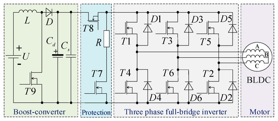
Figure 1.
The topology of a boost converter-fed brushless DC (BLDC) motor.
Figure 2 shows the operating principle of a Y-connected windings BLDC motor in a clockwise cycle, including the conduction sequence, current flow direction, waveforms of induced electromotive forces (EMFs) and currents, along with hall signals (HA, HB, HC). An electrical cycle of a BLDC motor can be divided into six different switching states. In each state, a different pair of MOSFETs conducts and two phases energize while leaving the third floated.
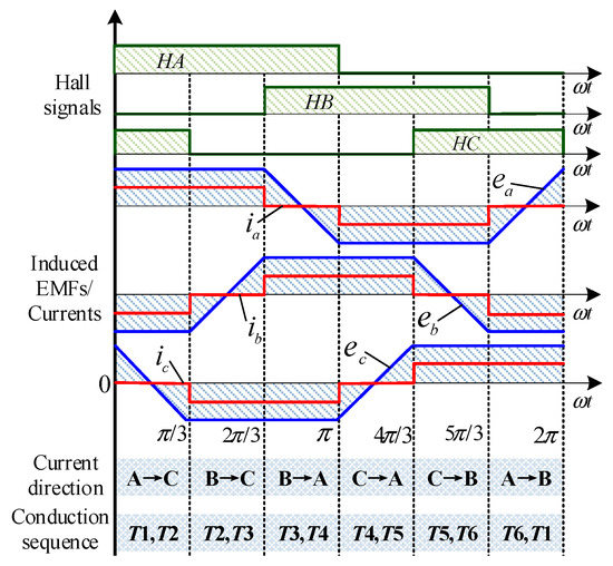
Figure 2.
Operating principle in the clockwise cycle.
In the presented work, the following assumptions are used for simplification: (1) the air gap magnetic field distribution is square wave, and magnetic hysteresis, saturation and eddy losses are ignored [15]; (2) Y-connected stator windings are symmetrical, and their resistance and inductance are constant. A group of first-order differential equations with state variables is used to set up the simulation model of the machine. The state equations of a BLDC machine can be obtained by the algebraic transformation of the conventional differential equation model. The fourth-order state equation of the BLDC motor can be expressed as
where iA, iB and iC are the phase-current, uA, uB and uC are the phase voltages, R is the phase resistance, L is the self-inductance, M is the mutual inductances between phases, ψpm is the permanent magnet flux-linkage, θ is the rotor position angle, TL is the load torque, Ω is the angular velocity of rotation, p is the number of pole-pairs, J is the moment of inertia and BV is the coefficient of viscosity. In Equation (4), the PM flux linkage ψpm(θ) is only a function of θ, which can be regarded as a coefficient of the equation. The ψpm(θ) has the same shape with induced EMF, as shown in Figure 2, and its magnitude can be obtained from induced EMF by utilizing a finite element field analysis or test. The waveform data of ψpm(θ) are stored in central processing unit (CPU) and the lookup table (LUT) method is adopted to obtain them according to the angle detected by a position sensor.
The boost converter is a kind of single pipe non-isolated DC conversion circuit, which is mainly composed of four parts: power device, diode, filter capacitance and energy storage inductance. Its operating modes can be divided into two categories: continuous current mode (CCM) and discontinuous current mode (DCM) [20].
Under the CCM condition, the boost converter-fed BLDC motor operates in two states and the state–space equations can be expressed as [21]
where D is the duty cycle, x is the state variable, x = (iL uC), is the differential of the state variable, iL is the inductance current, uC is the capacity voltage, ui is the input voltage, and A1, A2, B1 and B2 are the coefficients related to the circuit structure. The state–space equation can be obtained by
where A = DA1 + (1 − D)A2, B = DB1 + (1 − D)B2. Figure 3 shows the equivalent circuits when the switch T9 is on and off, respectively, regardless of the protection circuit. Using the state-space averaging method, the converter is transformed into an equivalent linear, time-varying, continuous circuit. When switch T9 is ON, the state–space equations are shown, ignoring the resistance of diode D and switch T8 [22,23]:

Figure 3.
The equivalent circuit of the combination. (a) T9 is on. (b) T9 is off.
In case the switch is OFF, the state–space equations are given by
Using the state–space averaging method these equations can be shown by
where uin and uout are the input and output voltages of the boost converter, L is the energy storage inductance, C is the filter capacitance, D is the duty cycle of switch T9, iL is the inductance current, R is the single-phase resistance, including stator resistance and transistor on-resistance. Ignoring the resistance of switch T8, it can be rewritten as:
According to the design requirements of the system, the specifications of the front-end boost converter can be obtained by
where ΔiL and Δu are the current and voltage ripples, respectively, R’ is the load resistance, and fs is the switch frequency of power device T9. Here L takes 3.5 mH and C takes 200 μF according to the requirements of the system. These equations are utilized to set up the simulation model of the machine and the converter, offering the design parameter reference and supports for the prototype.
To gain an optimized dynamic response, the bus-voltage should be kept at a high level by utilizing the boost converter. As mentioned above, the output voltage of the converter adopted only two levels. The DC-link voltage states u1 and u2 can be obtained according to the logical synthesis operation of control factors including S, K1, K2 and K3, as shown in Table 1. The operating logic results are stored in a digital signal processing (DSP) chip and the reference LUT method is adopted according to the requirements under different situations during operation. This method can reduce the cost of the chip compared with the on-line control method and improve the reliability of the program.

Table 1.
The boost converter operating logic.
Here, “u1 = 1” and “u2 = 1” represent that the DC-link voltage equals to 270 and 300 V, respectively, S is the current operation state of the BLDC machine, K1 is the manual control signal state, K2 is the overlarge load variation situation, and K3 is the current DC-link voltage state. It can be found that S has the highest control priority, which means that the boost circuit has the chance to work only under the condition of “S = 1.” Therefore, there is no need for the supply voltage to be adjusted, and the protection circuit will take over the system under faulty situations. The DC-link voltage will be boosted to 300 V, an over-rated but relatively safe level, when the manual control signal is triggered or when load variation is too large. This results in an increase in machine speed for a short period. To gain a clear explanation, the results of LUT can be summarized using Equation (14):
Note that the accelerate state should not be too long, as it keeps the machine under the over-rated stage. Meanwhile, the voltage will maintain at the rated value of 270 V when the supply voltage falls, regardless of the manual control signal. When an abrupt load and a voltage drop occur simultaneously, the voltage will be regulated to 300 V. The over-voltage and under-voltage threshold value are set to 320 and 200 V, respectively, to ensure the safety of the system and a relatively wide adjustment range of the boost converter. The protection circuit will operate if the boost converter adjustment cannot make up the falling voltage; otherwise, the circuit will not be involved.
3. Control System Design
Figure 4 shows the block diagram of the proposed boost converter-fed BLDC machine control system, which is composed of a power circuit, a control circuit and a remote monitoring circuit. The power circuit mainly deals with the driving and commutating of the boost converter-fed BLDC machine according to the control signals. The control circuit, the key to the system, is mainly responsible for power management, conditioning and sampling, isolation and protection, and digital signal processing (DSP). The power management circuits convert 270 V DC bus-voltage to different required levels according to the distribution scheme of the system. The conditioning and sampling circuits realize the conversion from analog signals, such as current, voltage, and temperature, to digital signals through sensor detections, amplifiers, filters, and analog to digital converter (ADC) chips. The isolation and protection circuits are designed to realize electrical isolation between power and control parts. The hardware protection circuits consist of some comparators and a complex programmable logic device (CPLD). DSP is used to calculate the sampling output of ADC and realize the closed-loop control. The remote monitoring circuits realize the anti-interference data transmission between the personal computer (PC) and DSP by utilizing a series communication interface (SCI) and a shielded RS-485 transceiver.
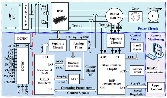
Figure 4.
Control block diagram.
To attain a small static tracing error, anti-disturbance ability, and rapid dynamic performance, the system adopts a control strategy that combines normal mode regulation with boost mode adjustment, as the block diagram shows in Figure 5.
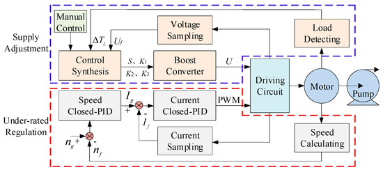
Figure 5.
Control strategy block diagram.
It can be seen from Figure 5 that the boost mode adjustment process consists of signal detection, control synthesis of S, K1, K2 and K3, and a DC-link voltage closed-loop calculation. It ensures a reliable power supply under over-load or under-voltage fault situations according to the Equation (11). Normal mode regulation deals with rated states by adopting a conventional dual closed-loop proportional integral derivative (PID) control strategy, which is still the workhorse in industries despite the great evolution and rapid development of hardware [24]. The outer loop is the speed loop, which adopts proportional integral (PI) action, aimed at stabilizing speed and resisting load-disturbance. In contrast, the inner current loop adopts P action to deal with current stabilization and voltage-fluctuation resistance. Voltage, current and load torque are detected by corresponding sensors and converted into digital signals using A/D sampling circuits. Angular speed is calculated by hall signals utilizing event capture (eCAP) module of the DSP chip. The manual control signal is the backup control signal of the boost converter for debugging. There is almost no need for the BLDC machine here to adopt the flux-weakening control method. On one hand, this system is for an aerospace oil pump and the flux-weakening region does not suit the requirements of such pumps. On the other hand, the drive system may suffer from a flux-weakening failure, which may decrease the reliability of the whole system.
When a PID controller is utilized, it provides a pole and two negative real zeros for the system. The pole helps to improve the system order-type, eliminate or reduce the steady-state error, and improve the steady-state performance. The negative real zeros can increase the phase margin, adjust the relative stability, and improve the dynamic performance. Therefore, the control stability performance of the system and the bandwidth can be assured as long as there is a reasonable choice of controller parameters (Kp, Ki, Kd). Here Kp = 10, Ki = 0.01, Kd = 0.
4. Fault Protection Strategy
The protective circuits are designed to improve the reliability of the system. The protection measures are implemented by CPLD and switches T7 and T8. The protection signals, i.e., bus over-voltage (OV), bus under-voltage (/UV), bus over-current (BOC), and phase over-current (POC), are generated by hardware circuits and act as the inputs of CPLD. Filter operation and logic synthesis measures were taken in the CPLD program to export the fault protection operation signals of T7 and T8. The hardware description language VHDL was utilized to realize programming. Therefore, this hardware protection scheme can improve the reliability of the system compared with the software type. Meanwhile, unlike the cycle-by-cycle method, which takes protection measures at each cycle of the pulse width modulation (PWM) signal, the proposed scheme greatly reduces the cost of the chip.
4.1. Voltage Protection
• Bus over-voltage protection
When the bus–voltage exceeds Ur, an over-voltage signal is generated by a comparator. If the signal lasts longer than tr, switch T7 will be turned ON and the pumping voltage will discharge through the brake resistance R, as shown in Figure 6.
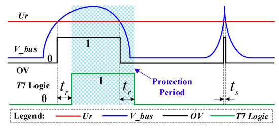
Figure 6.
Bus over-voltage protection logic.
Switch T7 should keep the conducted state for tr after the over-voltage signal disappears. The purpose of the conducted delay tr is to prevent the power device from switching frequently, which helps to reduce losses. However, the delay should not be too long otherwise the brake resistance will be too hot, which may lead to a low efficiency. In this paper, tr is taken to be 5 ms, which is programable according to the clock period. In order to eliminate the effect of signal jamming on system stability, a signal is recognized as a spike signal when the over-voltage period is less than ts, and can be ignored. Here, ts is taken to be 1 ms.
• Bus under-voltage protection
Figure 7 shows bus under-voltage protection control logic, and /UV is the protection signal. It is set to “1” when the system is under a normal state and “0” if the DC-link voltage is lower than a certain value. In order to eliminate the effect of a jamming signal, it is recognized as an interference signal when /UV lasts less than tr. Here, tr is taken to be 1 ms. If the /UV signal lasts longer than ts, MOSFET T8 will be switched OFF and the drive system will be disconnected from the boost converter to prevent a second over-current fault. When the /UV signal disappears, T8 keeps the cutoff state for ts before it is back to power. It is noted that the boost converter will take over to regulate the voltage back to normal during ts. In this paper, ts is taken to be 50 ms.
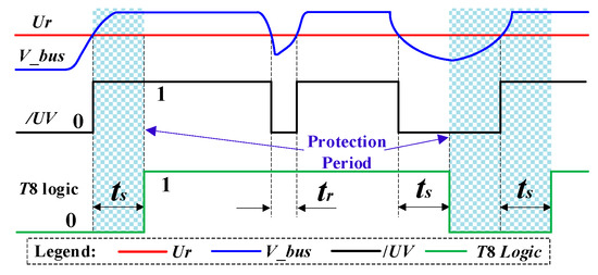
Figure 7.
Bus under-voltage protection logic.
4.2. Current Protection
• Bus over-current protection
In extreme cases, such as starting with a heavy load or stalling in a short time, the peak of bus-current may increase to a very large value. The system requires instantaneous protective action under these circumstances, which is called bus over-current transient protection. In contrast, the protective action dealing with a current increase caused by long-time overload is called bus over-current locked protection. In order to reduce switching noise and loss, the protection circuit should not be under frequent operation.
Figure 8a shows the bus over-current transient protection logic. BOC1 stands for hardware input protection signal, which is “0” under a normal state and “1” when the DC-link current is over 100 A. The protection measure varies with ts, which is the duration of BOC1. It can be divided into three cases: (1) when t > ts > tr, switch T8 shuts off instantly and keeps this state until t; (2) when ts ≤ tr, the signal is considered as a spike and the protection action will not be triggered; (3) when ts ≥ t, switch T8 shuts off until BOC1 is back to “0” level. In this work, t and tr are taken to be 5 and 1 ms, respectively.
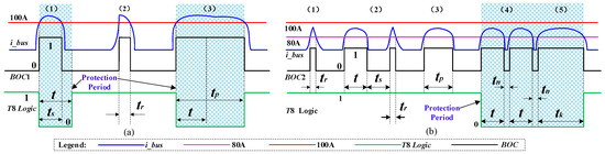
Figure 8.
Bus over-current protection logic. (a) Transient protection; (b) locked protection.
Bus over-current locked protection logic is shown in Figure 8b. BOC2 represents the hardware input protection signal, which is “0” under a normal state and “1” when the DC-link current is over 80 A. The protection measure can be divided into five categories varying with tp, the duration of BOC2: (1) when tp ≤ tr, it is considered to be an interference; (2) when 2t ≥ tp ≥ t, the signal shows again after the interval time ts (ts > tr), and if its duration tp ≤ tr, the protection does not take effect; (3) when 2t ≥ tp ≥ t, the protection does not carry on; (4) when tp ≥ t, the signal shows again after the interval time tn (tn ≤ tr), but if its duration tp ≥ t, switch T8 shuts off until the signal returns to “0”; and (5) when tp ≥ 2t, switch T8 shuts off until BOC2 returns to “0.” Here, t and tr are taken to be 5 and 1 ms, respectively.
• Phase over-current protection
Short-circuit faults of machine windings may result in phase over-current faults. Their protection logic is shown in Figure 9, including two cases: (1) if the peak of phase-current exceeds ir, T8 shuts off to cut off the drive system from the power source. When the signal is normal, T8 turns on after a duration tr. The purpose of the delay is to prevent excessive loss and influence on the rapidity of the system; (2) if the peak of phase-current continuously exceeds is but is below ir for at least ts, T8 will turn off and lock the state. However, if the over-current state lasts no longer than ts, the signal is negligible. In this work, ts, tr, is, and ir are taken to be 5 ms, 10 ms, 150 A, and 190 A, respectively.
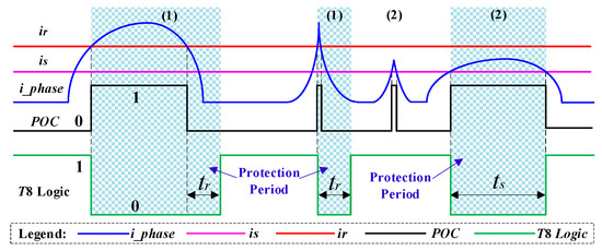
Figure 9.
Phase over-current protection logic.
5. Experimentation
5.1. Prototype and Experimental Scheme
A 3-phase 2-pole BLDC machine was designed and manufactured by the aviation industry corporation who offered this research subject. A simulation model for the control system was established in Simulink. The specifications of the machine are tabulated in Table 2. The experimental prototype and the required equipment are shown in Figure 10.
Table 2.
The BLDC machine specifications.
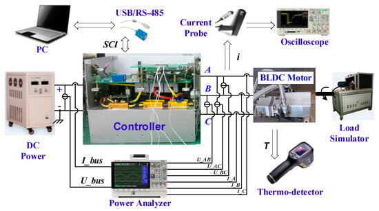
Figure 10.
Prototype and the required equipment.
The controller contained two control boards: an interface board, a boost converter and other power devices. The intelligent power module (IPM) PM150RL1A060 was used, and other power switches adopted IGBT module CM150DY-24A. All of them were products of Mitsubishi. A floating-point DSP TMS320F28335 and a MAX-II series CPLD EPM1270 were employed to build a central controller unit using the proposed control and protection methods. The A/D sampling process was accomplished by an AD7329 chip and the sampling frequency was chosen to be 20 kHz. The driving and protection logics of the system which belonged to sequential statements was implemented in CPLD, and the dual closed-loops control method was carried out in DSP. In the testing, the BLDC machine was coupled to a load simulator. A power analyzer and an oscilloscope with a current probe were utilized to acquire experimental data. The data transmission between the controller and the PC through SCI was realized by a RS-485 transceiver. A thermo-detector was used to monitor and verify the sample temperatures of the controller and the machine.
5.2. Results and Discussions
5.2.1. Dynamic Response under Different Conditions
• Start-up process
A serious over-voltage phenomenon can also exist during the starting process. Appropriate adjustments of the boost converter can be made to meet critical acceleration requirements under rated conditions.
Figure 11 shows bus-voltage (red line) and phase A-current (blue line) waveforms of the normal mode and the manual boost mode (K1 = 1) in the starting and stable running processes under rated conditions. Here, the duty cycle of the inverter was set to 50% and the scaling of the signals is 50 V and 50 A, respectively. It was found that the impact currents of the two modes during the start-up process existed but were acceptable due to dual closed-loop control. The bus-voltage of the steady state stabilized around 270 V under the normal state and 300 V under manual boost mode. A reasonable bus pump-up-voltage of about 22 V existed during each transient process, which was due to the abundant filter capacitance and appropriate absorbing capacitance. The start-up period of the manual boost state lasted 2.95 s, which was 36.4% faster than the 4.64 s of the normal state. Therefore, the proposed topology had the ability to improve the start-up performance under K1 = 1 control conditions. The fluctuations and spike signals of the waveforms existed because of the PWM mode voltage source.
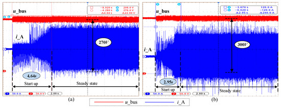
Figure 11.
Bus-voltage and phase-current waveforms in transient process. (a) Normal mode; (b) manual boost mode (K1 = 1).
• Speed adjustment process
Figure 12 shows the actual speed (Feedback) curve tracking the expected speed (Given) from 0 to 12,500 rpm. The given speed waveform was set up in a stepped pattern, and feedback data points were collected every 0.5 s. It was found that the actual speed tracked the given speed very well, verifying the validity of the dual closed-loop control strategy. The accelerating process contained two stages: the normal stage, from 2500 to 7500 rpm without boost converter during Δt1, and the manual boost stage with converter from 7500 to 12,500 rpm during Δt2. Considering the time consumption by series communication, closed-loop interrupt routine, and other programs, Δt1 needed about 3.9 s. It is noted that Δt2 lasted about 1.8 s, which was much shorter than Δt1, indicating that the K1 = 1 control state could shorten the speed tracking response time during steady state.
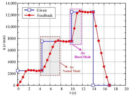
Figure 12.
Speed tracking curve.
• Abrupt load torque change process
The machine’s acceleration characteristic with load represents the load-disturbance resisting performance and affects the execution speed of the system. Figure 13 shows part of the machine’s phase-current waveforms for the normal state and adjustment state (K2 = 1) during the abrupt load torque change procedure from load No. 1 (1 N.m) to load No. 2 (3 N.m) under rated-voltage power supply. Here, the duty cycle of the inverter was set to 50%.
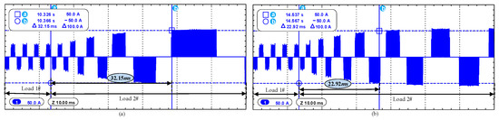
Figure 13.
Part of the phase-current waveforms during abrupt load torque change from 1 to 3 N.m. (a) Normal state; (b) adjustment state (K2 = 1).
It can be observed that the aptitude of the phase-current rose with load increase, while machine speed slowed down. The process of normal state under this large load variation situation lasted 2.1 s while the adjustment state lasted 1.4 s. The waveforms of these procedures were similar to the waveform of the start-up process. The phase peak current was about 25 A during the load torque change period. It took 32.15 ms for the phase peak current to rise from 25 to 50 A, as shown in Figure 13a. During actual operation, the boost circuit started to work under this impact load situation and K2 was set to “1.” This resulted in the period of the adjustment process being shortened. It took 22.92 ms for the phase peak current to rise from 25 to 50 A, as shown in Figure 13b, reflecting a relatively fast adjustment characteristic under the K2 = 1 state.
According to the aforementioned results, the dynamic response time of the normal mode and the boost mode with proposed methods are shown in Table 3. During the start-up and abrupt load torque change procedures, the response time of the boost modes are both shortened by about 1 s, which is almost 30% of the response time under normal conditions. The response time of the speed adjustment process is shortened by 2 s, which is due to the data transmission delay by the series communication interface.
Table 3.
The dynamic response time in different processes.
Compared with the conventional full bridge inverter, the proposed topology is able to improve the dynamic response characteristics significantly. Meanwhile, excessive elements and a complicated control strategy are avoided to achieve a wide range of speed control performances in comparison with BL-Zeta or BDC combinations. However, only certain voltage output levels of the converter should be allowed to avoid frequent switching operations.
5.2.2. Voltage Limits
Figure 14 shows the waveforms of bus-voltage and machine speed during the bus-voltage fault protection process.
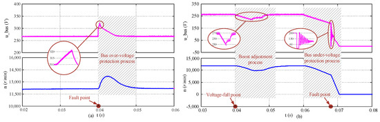
Figure 14.
Waveforms of bus-voltage and motor speed during the bus-voltage fault protection process; (a) over-voltage protection; (b) under-voltage protection.
It can be seen from Figure 14a that the fault point was set at 0.04 s, and the bus-voltage started to rise, resulting in the increase in speed. The protection action was triggered and switch T7 was conducted as soon as bus-voltage was up to 320 V, which led to decreases in voltage. Consequently, speed was back to the normal value. The power was cut off and the machine was shut down rapidly after an adjustment process when bus-voltage dropped to 200 V, as shown in Figure 14b.
What needs to be pointed out is that the boost converter started to work to make up the difference when bus-voltage fell (K3 = 1). Figure 14b shows that the boost converter pulled up the bus-voltage back to the rated level of 270 V quickly when it had not yet dropped to the protection threshold value of 200 V. As a result, the machine speed returned to the rated value and the system maintained normal performance despite the lower power supply. This process commonly helps to deal with under-voltage power faults without turning power off completely. Note that the dynamic period should be less than ts, or the under-voltage protection action will be triggered as well.
5.2.3. Current Limits
Figure 15 shows the bus-current and machine speed waveforms during the bus over-current fault transient and locked protection processes. It can be seen from Figure 15a that the bus-current rose to a fairly high level in a short period of time when fault No. 1 occurred, which was a risk factor for the system. This is commonly caused by a locked rotor without any protection. In contrast, the transient protection took over when fault No. 2 occurred and the power was cut off when bus-current rose to 100 A, resulting in a rapid decline in machine speed. The locked protection mainly dealt with bus over-current caused by an overload situation, as shown in Figure 15b. When fault No. 4 occurred, the bus-current rose to 80 A and kept that state for at least tk. Then, the protection action started to work and power was switched off. However, the system neglected fault No. 3 for a short period.
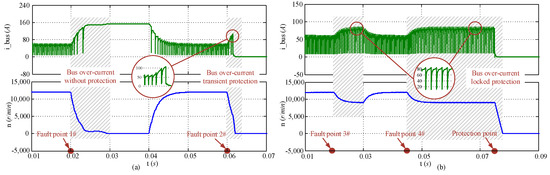
Figure 15.
Waveforms of bus-current and motor speed during bus over-current fault protection processes; (a) transient protection; (b) locked protection.
A phase over-current fault is commonly caused by a winding short-circuit. Figure 16 shows the phase-current and machine speed waveforms during the phase over-current fault protection process. Analyzing the waveforms, current and speed were smooth and stable before the fault occurred. As soon as the fault took place, the current waveform increased rapidly with a serious distortion and machine speed fell, accompanied by violent oscillations. Some relevant protective measures should be taken to fit the secure operation of the machine under this condition. When fault No. 5 occurred, the phase-current rose to protection threshold value is, i.e., 150 A, and the protection circuit cut off the bus power instantly, resulting in a rapid decline in machine speed. However, the switch T8 was conducted again as soon as the fault signal disappeared, and the system went back to normal operation. In contrast, the phase-current and machine speed dropped to 0 quickly, after a short dynamic adjustment period when the phase-current increased to ir of 190 A, preventing the asymmetric operation and windings from being damaged by over-heating.
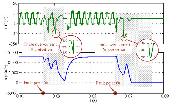
Figure 16.
Waveforms of phase-current and motor speed during phase over-current fault protection process.
6. Conclusions
This paper proposes a model-based optimized PM BLDC machine topology for dynamic response enhancement and fault protection improvement. In the proposed topology, the boost converter ensures a reliable power supply under over-load or under-voltage fault situations while protective circuits, including bus over-voltage, under-voltage, bus over-current, and phase over-current protection, are designed to improve the reliability of the system. The corresponding drive logic, control method and protection strategy are developed for an aeronautical fuel pump. A control strategy is designed, which combines normal dual closed-loop regulation with boost adjustment to attain a small static tracing error, anti-disturbance ability and rapid dynamic performance. A simulation model and experimental prototype are constructed and manufactured to validate the proposed topology and control method for an aeronautical fuel pump system.
In conclusion, the proposed method has the following advantages:
- (1)
- During the start-up and abrupt load torque change procedures, the response time is shortened by about 30% of the conventional full-bridge inverter.
- (2)
- The voltage and current limits under different situations prove that the proposed strategy could increase operational reliability.
- (3)
- Both simulation analysis and experimental research verify that the response performance is significantly improved, and the protection capability is enhanced.
- (4)
- The proposed strategy can be extended more generally to any voltage supply machine. Possible further investigations may include an alternative converter and an advanced control method validation for dynamic performance.
Author Contributions
W.W. was in the charge of conceptualization, methodology and investigation. J.W. performed data curation. The original draft was written by W.W. and revised by J.W. Both authors were involved in preparing the final version of this manuscript.
Funding
This research was funded by the Scientific Research Projects of Inner Mongolia Autonomous Region (NJZY17409) and Scientific Research Projects of Ordos Institute of Technology (KYYB2018007).
Acknowledgments
The authors would like to thank the editor and the anonymous reviewers for the comments and suggestions.
Conflicts of Interest
The authors declare no conflicts of interest.
References
- Xia, C.L. Permanent Magnet Brushless DC Motor Drives and Controls; Science Press: Singapore, 2012. [Google Scholar]
- Changliang, X.; Hongwei, F. Permanent magnet brushless dc motor and its control. J. Electr. Technol. 2012, 27, 25–34. [Google Scholar]
- Jones, R.I. The more electric aircraft: The past and the future? In Proceedings of the IEE Colloquium on Electrical Machines and Systems for the More Electric Aircraft, London, UK, 9 November 1999; pp. 1–4. [Google Scholar]
- Romeral, L.; Rosero, J.A.; Espinosa, A.G.; Cusido, J.; Ortega, J.A. Electrical monitoring for fault detection in an EMA. IEEE Aerosp. Electron. Syst. Mag. 2010, 25, 4–9. [Google Scholar] [CrossRef]
- Bose, B.K. Power electronics and motor drives recent progress and perspective. IEEE Trans. Ind. Electron. 2009, 56, 581–588. [Google Scholar] [CrossRef]
- Elbuluk, M.E. Motor drive technologies for the power-by-wire (PBW) program: Options, trends and tradeoffs part.1 motors and controllers. IEEE Aerosp. Electron. Syst. Mag. 1995, 10, 37–42. [Google Scholar] [CrossRef]
- Yue-yun, C.; Wei-zhong, G.; Feng, G. NURBS-Based Feature Modeling and Trajectory Planning for Ram Motion of Servo Mechanical Presses. J. Shanghai Jiaotong Univ. 2009, 43, 138–139. [Google Scholar]
- Pellegrino, G.; Jahns, T.M.; Bianchi, N.; Soong, W.L.; Cupertino, F. The Rediscovery of Synchronous Reluctance and Ferrite Permanent Magnet Motors: Tutorial Course Notes; Springer: Berlin, Germany, 2016. [Google Scholar]
- Churn, P.M. Electro-hydraulic actuation of primary flight control surfaces. In Proceedings of the All Electric Aircraft, London, UK, 17 June 1998; pp. 3/1–3/5. [Google Scholar]
- Huang, X.Y.; Goodman, A.; Gerada, C.; Fang, Y.T.; Lu, Q.F. A single sided matrix converter drive for a brushless DC motor in aerospace applications. IEEE Trans. Ind. Electron. 2012, 59, 3542–3552. [Google Scholar] [CrossRef]
- Fang, J.; Li, W.; Li, H.; Xu, X. Online inverter fault diagnosis of buck-converter BLDC motor combinations. IEEE Trans. Power Electron. 2015, 30, 2674–2688. [Google Scholar] [CrossRef]
- Bist, V.; Singh, B. A reduced sensor PFC BL-Zeta converter based VSI fed BLDC motor drive. Electr. Power Syst. Res. 2013, 98, 11–18. [Google Scholar] [CrossRef]
- Abdi, B.; Teymoori, M.M.; Gholamrezaei, H.; Nasiri, A.A. A simple analog BLDC drive control for electro-mechanical energy storage system. Energy Procedia 2011, 12, 1002–1007. [Google Scholar] [CrossRef]
- Hosseini, S.H.; Nejabatkhah, F.; Niapoor, S.A.K.M.; Danyali, S. Supplying a brushless dc motor by z-source PV power inverter with FL-IC MPPT. In Proceedings of the International Conference on Green Circuits and Systems, Shanghai, China, 21–23 June 2010; pp. 485–490. [Google Scholar]
- Niapour, S.; Danyali, S.; Sharifian, M.B.B.; Feyzi, M.R. Brushless DC motor drives supplied by PV power system based on Z-source inverter and FL-IC MPPT controller. Energy Convers. Manag. 2011, 52, 3043–3059. [Google Scholar] [CrossRef]
- Zahab, E.E.A.; Zaki, A.M.; El-Sotouhy, M.M. Design and control of a standalone PV water pumping system. J. Electr. Syst. Inf. Technol. 2016, 4, 322–337. [Google Scholar] [CrossRef]
- Akkaya, R.; Kulaksiz, A.A.; Aydogdu, O. DSP implementation of a PV system with GA-MLP-NN based MPPT controller supplying BLDC motor drive. Energy Convers. Manag. 2007, 48, 210–218. [Google Scholar] [CrossRef]
- Kumar, R.; Singh, B. Grid interfaced solar PV powered brushless DC motor driven water pumping system. In Proceedings of the 2016 7th India International Conference on Power Electronics, Thapar Univ, Electr & Instrumentat Eng Department, Patiala, India, 17–19 November 2016; pp. 1–5. [Google Scholar]
- Gopinath, M.; Yuvaraja, T.; Jeykumar, S. Implementation of four quadrant operation of BLDC motor using model predictive controller. In Proceedings of the Materials Today, Ongole, India, 29–30 July 2016; pp. 1666–1672. [Google Scholar]
- Abraham, I.; Pressman, K.B. Taylor Morey. In Switching Power Supply Design, 3rd ed.; McGraw-Hill: New York, NY, USA, 2009. [Google Scholar]
- Mahdavi, J.; Emadi, A.; Toliyat, H.A. Application of state space averaging method to sliding mode control of PWM DC/DC converters. In Proceedings of the Conference Record of the 1997 IEEE Industry Applications Conference Thirty-Second IAS Annual Meeting, New Orleans, LA, USA, 5–9 October 1997; pp. 820–827. [Google Scholar]
- Feng, J.; Liu, K.; Wang, Q. Scheme based on buck-converter with three-phase H-bridge combinations for high-speed BLDC motors in aerospace applications. IET Electr. Power Appl. 2018, 12, 405–414. [Google Scholar] [CrossRef]
- Lehman, B.; Bass, R.M. Extensions of averaging theory for power electronic systems. IEEE Trans. Power Electron. 1996, 11, 542–553. [Google Scholar] [CrossRef]
- Yu, C. Autotuning of PID Controllers, a Relay Feedback Approach, 2nd ed.; Springer: Berlin, Germany, 2006. [Google Scholar]
© 2019 by the authors. Licensee MDPI, Basel, Switzerland. This article is an open access article distributed under the terms and conditions of the Creative Commons Attribution (CC BY) license (http://creativecommons.org/licenses/by/4.0/).