Review

Atomic Layer Deposition of Inorganic Thin Films on 3D Polymer Nanonetworks

1
School of Materials Science and Engineering, Kumoh National Institute of Technology, Gumi, Gyeongbuk 39177, Korea
2
Engineering Ceramic Center, Korea Institute of Ceramic Engineering, Icheon, Gyeonggi 17303, Korea
3
Department of Materials Science and Engineering, Korea Advanced Institute of Science and Technology, Daejeon 34141, Korea
*
Author to whom correspondence should be addressed.
Appl. Sci. 2019, 9(10), 1990; https://doi.org/10.3390/app9101990
Submission received: 19 March 2019 / Revised: 24 April 2019 / Accepted: 30 April 2019 / Published: 15 May 2019
(This article belongs to the Special Issue Atomic Layer Deposition for the Synthesis of Thin Films)

Abstract

:
Atomic layer deposition (ALD) is a unique tool for conformally depositing inorganic thin films with precisely controlled thickness at nanoscale. Recently, ALD has been used in the manufacture of inorganic thin films using a three-dimensional (3D) nanonetwork structure made of polymer as a template, which is pre-formed by advanced 3D nanofabrication techniques such as electrospinning, block-copolymer (BCP) lithography, direct laser writing (DLW), multibeam interference lithography (MBIL), and phase-mask interference lithography (PMIL). The key technical requirement of this polymer template-assisted ALD is to perform the deposition process at a lower temperature, preserving the nanostructure of the polymer template during the deposition process. This review focuses on the successful cases of conformal deposition of inorganic thin films on 3D polymer nanonetworks using thermal ALD or plasma-enhanced ALD at temperatures below 200 °C. Recent applications and prospects of nanostructured polymer–inorganic composites or hollow inorganic materials are also discussed.

Graphical Abstract

1. Introduction

Atomic layer deposition (ALD), a type of chemical vapor deposition (CVD), is a unique thin film deposition technique that can control the thickness of thin films at the angstrom level based on sequential self-limiting, gas-solid surface reactions [1,2,3]. One of the key features of ALD is the ability to form a conformal thin film insensitive to surface topology, because the principle of ALD depends on surface adsorption. This results in excellent step coverage even for trench structures with extremely high aspect ratios, which is useful for semiconductor devices [4,5]. Another feature of ALD is that it is capable of low-temperature processing compared to other vapor-phase deposition techniques [6]. If precursors and systems are designed well-enough to allow the process temperature to be below 200 °C, then ALD can be applied to polymer substrates as well.
In recent years, the potential of ALD based on these benefits has expanded to nanotechnology [7]. As a representative example, ALD has been combined with three-dimensional (3D) polymer nanostructuring methods such as electrospinning, block-copolymer (BCP) lithography [8,9,10,11,12], direct laser writing (DLW) [13,14,15,16,17], multibeam interference lithography (MBIL) [18,19,20], and phase-mask interference lithography (PMIL) [21,22,23,24,25,26,27,28,29,30]. These unconventional nanofabrication techniques specialize in the production of 3D polymer nanonetworks that can serve as templates for subsequent material conversion processes [31]. Polymer templates have the advantage of being easily removed by thermal treatment, chemical dissolution, or plasma etching, unlike metal or ceramic templates, which require the use of hazardous acid solutions [32]. In polymer template-based strategies, ALD can be used for various purposes, such as (a) modifying the surface of the polymer template from hydrophobic to hydrophilic [23], (b) reducing the porosity of the polymer template [18], (c) adjusting the optical or mechanical properties of the polymer template [14,26], and (d) producing hollow inorganic materials converted from the polymer template [15,16,21,22,27,33].
An important technical requirement for depositing inorganic thin films on 3D polymer nanonetworks through ALD, which serve as templates, is to maintain the least-possible process temperature below the melting point of the polymer template to protect the 3D nanostructures during the process. For example, an epoxy-based negative-tone photoresist called an SU-8 (Microchem Co.) is widely used to prepare 3D nanostructured polymer templates through lithographic techniques because of advantages including excellent mechanical stability (E~2 GPa), high photosensitivity and resolution, and a thick film processing ability above several hundred microns [34]. However, because the glass transition temperature (Tg) of SU-8 after cross-linking is only ~200 °C, subsequent processes with SU-8 templates should be performed below Tg to prevent a reflow phenomenon. Most nanostructured polymer networks produced by other techniques also have poor heat resistance [35,36]. Therefore, to realize various materials and properties through 3D polymer template-based ALD, it is very important to secure a variety of methods for depositing inorganic thin films at temperatures below 200 °C, especially at room temperature.
This short review focuses on recent cases of successful formation of conformal inorganic thin films on 3D nanostructured polymer templates, using thermal or plasma-enhanced ALD (PEALD) at process temperatures below 200 °C (Figure 1a–c). We also discuss the material properties, applications, and prospects of 3D nanostructured inorganic or composite materials through this strategy.

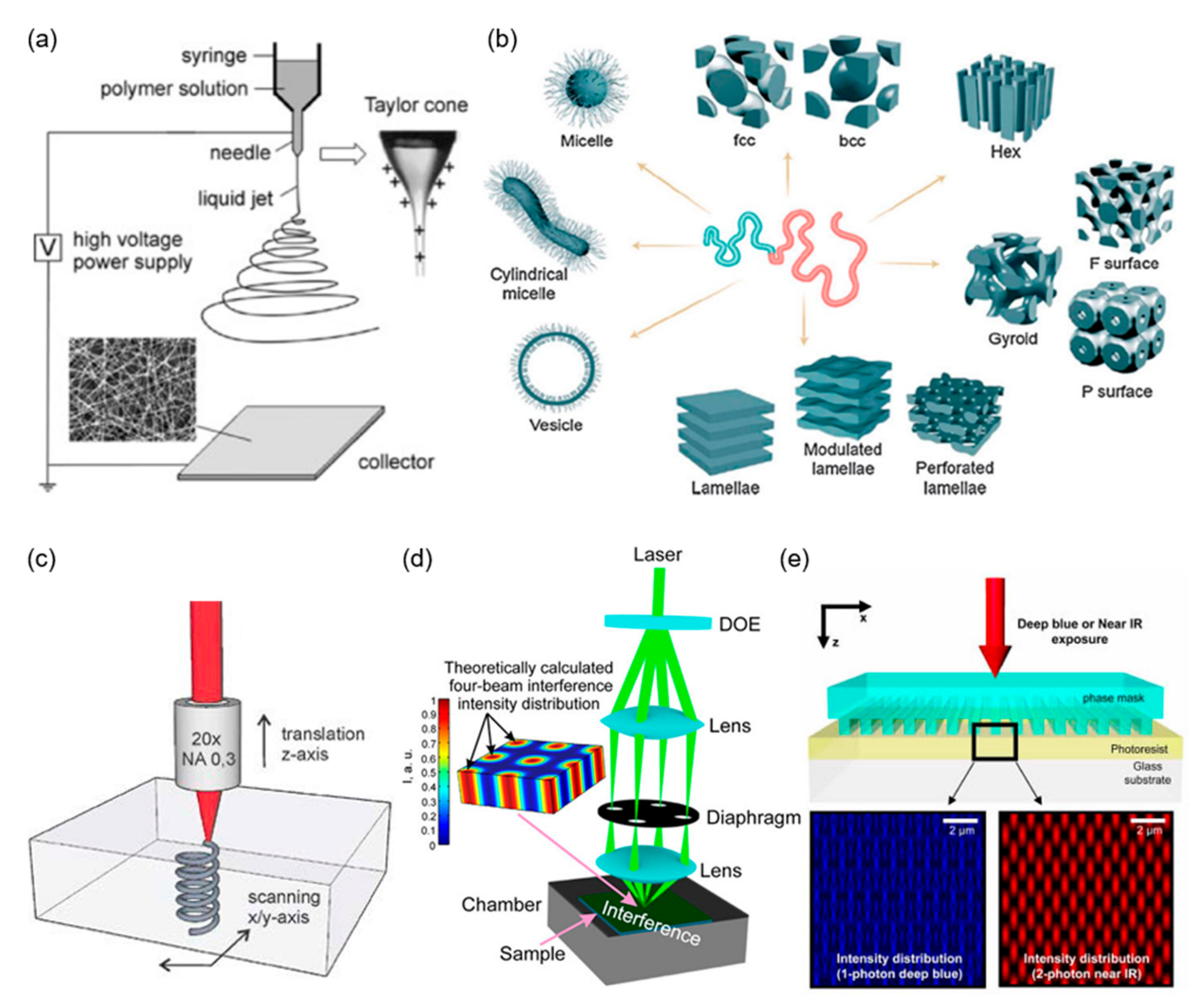
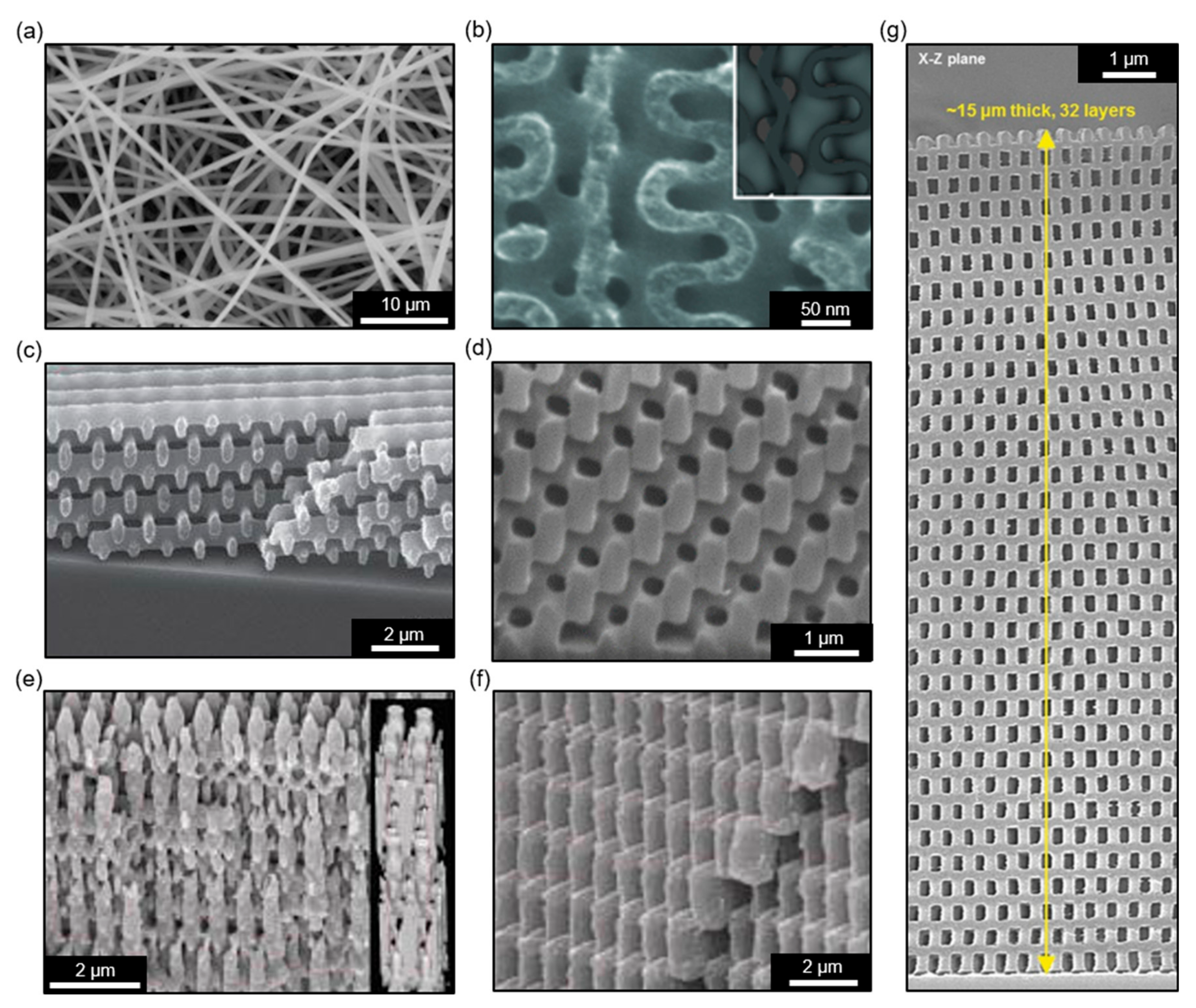
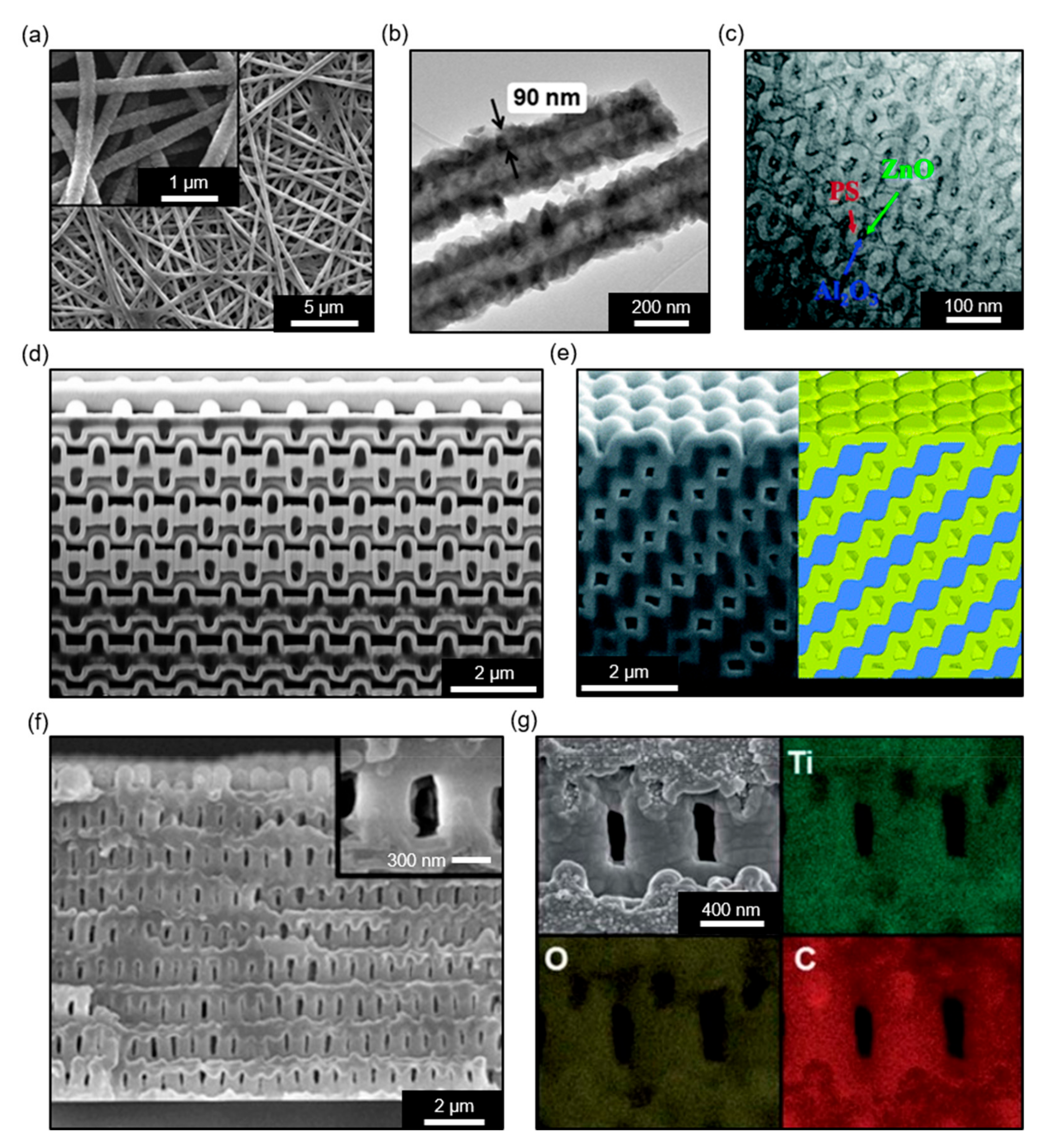
2. Preparation of 3D Polymer Nanonetworks

The 3D nanonetwork-structured polymer template can be divided into two types depending on the regularity of the structure (Figure 1b,c). For example, electrospinning is a typical technique to fabricate irregular 3D polymer nanonetworks over large areas [37,38,39,40]. Although electrospinning is an old technique, it is still the most powerful technique for the mass production of polymer nanonetworks. Most nanofibrous fabrics are made using this technique. The electrospinning system generally consists of a syringe pump that can push out a polymer solution, a DC high-voltage generator, a needle for extracting nanofibers, and a grounded collecting plate (Figure 2a). The polymer solution located at the end of the capillary forms a hemispherical droplet based on the equilibrium between gravity and surface tension. When an electric field is applied, a charge or dipole orientation is induced at the interface between the air and the droplet, creating an electrostatic repulsive force opposite to the surface tension. Thus, the hemispherical surface of the solution at the tip of the capillary stretches into a conical shape known as a Taylor cone. At the threshold voltage, the electrostatic repulsive force overcomes the surface tension, and a jet of polymer solution is ejected from the Taylor cone. In the case of a polymer solution with a sufficiently high viscosity, the charged jet ejects towards the collecting plate without collapsing. The jet trajectory can bend or change direction during flight. The jet is tapered in flight and the initial jet is split into several smaller filaments by electrostatic repulsion because the charge is concentrated on the surface. The solvent is evaporated during the flight and solid-phase polymer nanofibers are continuously deposited on the collecting plate. Electrospinning can control the diameter and density of 3D polymer nanonetworks by adjusting process parameters such as viscosity or surface tension of the solution, distance from the capillary tip to the collecting plate, applied voltage, and spinning time. A typical electrospun product is a nonwoven mat of randomly oriented fibers due to whipping instability. In some cases, extra auxiliary forces are used to align the nanofibers in a two-dimensional (2D) plane [41]. However, accurate vertical alignment between layers for constructing regular 3D nanonetworks is still difficult to achieve through electrospinning.
Polymer templates with regular or periodic 3D nanonetwork structures can be prepared using unconventional lithographic techniques. First, BCPs have been extensively investigated in the interest of generating polymer templates because of their ability to self-assemble into various types of periodic nanostructures, depending on their composition and molecular weight (Figure 2b) [42]. In particular, a gyroid structure can be created by using a BCP designed to self-assemble in 3D. For example, a polystyrene-based gyroid structure can be fabricated from the self-assembly of degradable block copolymers and polystyrene-b-poly(L-lactide) (PS-PLLA), followed by the hydrolysis of PLLA blocks [43]. BCP is advantageous in that it can easily manufacture periodic 3D polymer nanonetworks without expensive or complicated facilities. However, because it is based on a solution process, the precision and reproducibility of the structure are inferior.
Next, DLW based on two-photon polymerization is a well-known 3D printing technology that allows the construction of nanostructures with sub-100-nm resolution (Figure 2c) [44]. An ultrafast high-power laser beam is tightly focused within the volume of a transparent photopolymer, and the photopolymer is locally polymerized by absorbing one or more photons simultaneously. As the laser beam travels along the path designed using computer-aided design (CAD) or computer-aided manufacturing (CAM), a 3D ultrafine object is created by the solvent after the development process. While DLW has great advantages in manufacturing arbitrary structures with a high resolution, it suffers from fatal drawbacks such as a very slow production speed and the development of two-photon absorbing materials that are not diversified.
In this respect, MBIL, also called holographic lithography, is a precise manufacturing technique for periodic 3D nanonetwork structures, which complements the low productivity of DLW (Figure 2d) [49,50,51,52]. The principle of MBIL is to transfer the 3D periodic intensity distribution resulting from the interference between four coherent beams separated by a single laser, to photosensitive polymer. Various types of periodic structures can be created by adjusting the optical parameters (e.g., incident angle or polarization) of the four interfering beams. Because this method is a parallel process, unlike DLW, which is a serial process, it has advantages in terms of the large-scale fabrication of periodic 3D nanonetworks; however, the degree of structural freedom is not high. Moreover, because the four interfering beams must be temporally and spatially coherent to generate interference, the structural reproducibility is very sensitive to vibration, and inevitably requires a complex optical setup.
To evolve into more industrial processes, Jeon et al. developed PMIL, also known as proximity-field nanopatterning (PnP), in which all complex interference optics are integrated into a single conformal phase-mask (Figure 2e) [23,37,48,53,54,55,56,57,58]. The principle of this technique is to imprint the Talbot interference, caused by the interference of diffractions arising from the phase mask with the surface relief structure, onto the photopolymer. The used phase-mask is generally made of a poly(dimethylsiloxane) (PDMS)-based elastomer, which can adhere to the substrate without being sensitive to surface roughness, thereby enabling high-resolution contact-mode lithography with high-vibration tolerance. The generated Talbot interference and 3D periodic nanonetworks can be varied by adjusting the incident wavelength of the laser and phase-mask geometry, and can be predicted and designed by optical simulations such as finite-difference time domain (FDTD), finite element modeling (FEM), or rigorous coupled-wave analysis (RCWA) [59]. Above all, PMIL has the advantage of expanding the production area of the 3D periodic nanonetwork to the wafer scale by increasing the size of the phase mask and exposure source. However, the existing technical issue is to improve the degree of structural freedom through an inverse algorithm design [60,61].
More information on the recent progress of the 3D nanofabrication techniques mentioned above can be found in the literature [13,30,51,62,63,64,65,66,67,68]. Figure 3 shows the representative examples of polymer templates with a regular or irregular 3D nanonetwork structure fabricated by the above 3D nanofabrication techniques, including electrospinning, BCL, DLW, MBIL, and PnP.

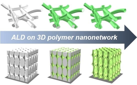
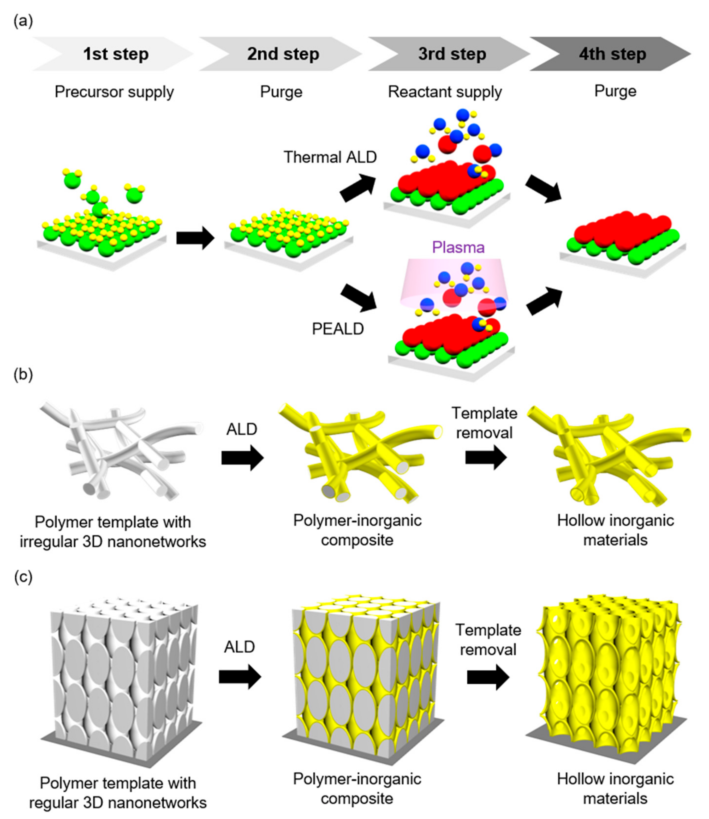
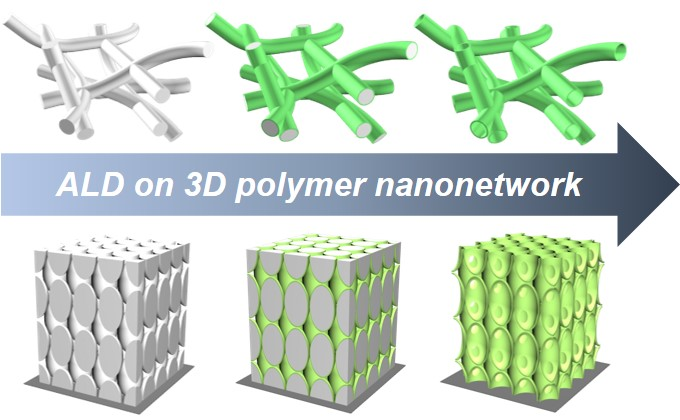
3. Conformal Deposition of Inorganic Thin Films on 3D Polymer Nanonetworks

The above-mentioned 3D nanofabrication techniques mainly produce polymer-based nanonetwork structures. However, to apply such nanostructured materials to various fields, it is necessary to compensate for the relatively poor thermal or mechanical resistance of the polymer, or to impart additional functionality (e.g., conductivity, reactivity, etc.). To achieve this, many studies have been performed to fill the interconnected pores of 3D nanonetworks with functional inorganic materials, including metals and ceramics [31]. Typical filling methods include electrochemical deposition, sol-gel reaction, and CVD. However, these bottom-up filling techniques eliminate the porous structure of 3D nanonetworks in a composite state. The removal of polymer templates by a high-temperature (>450 °C) heat treatment or an O2 plasma etching process allows an inverse porous structure; however, it is generally difficult to obtain high porosity (>90%). In contrast, ALD has a unique feature of the conformal coating of the surfaces of porous structures based on surface adsorption and reaction. In this case, we can selectively change surface properties or reduce pore size while maintaining a porous structure. Unlike bottom-up filling, ALD generates a hollow structure after removing the polymer template, thereby creating an ultra-lightweight and highly porous material similar to aerogel [29,70].
A conventional thermal ALD process begins when a precursor is fed into a chamber and adsorbed onto a polymer template. At this time, the substrate temperature should be maintained below the dissociation temperature of the precursor to prevent undesirable thin film formation. The dissociation temperature of the precursor ranges from about 100 to 700 °C, depending on the type of precursor. In polymer template-assisted ALD, a temperature of about 200 °C or less is preferred to prevent reflow of the polymer, even if the film quality deteriorates. The precursor is generally delivered to the polymer template with a carrier gas and adsorbed on the substrate by chemical attraction. To improve the uniformity of the thickness of the deposited film, a sufficiently long supply time is required to cover the nanoporous structure completely with the precursor at this stage [23,70,72]. In the next step, it is necessary to supply the purge gas to wash away the remaining precursor. Ar, an inert gas that does not react with the precursor, is generally used as the purge gas. Once the precursor supply is stopped and the purge gas is supplied, the remaining gaseous precursor in the chamber and the precursor adsorbed weakly on the template are rinsed away by the purge gas, leaving only one layer of the precursor that has been in strong chemical bonding with the template. A third step in the ALD process is the supply of reactants to the precursor-coated polymer template. The reactant chemically reacts with the precursor adsorbed on the template to form a thin film. Except for some precursors that require thermal activation, most precursors react spontaneously with the reactants even at room temperature. Heating is sometimes required to improve the properties and crystallinity of the deposited materials. When a metal oxide-based dielectric film is deposited, water is usually used as the reactant. However, when water is adsorbed on the inner wall of the chamber, water may easily condense, and the condensation may not be removed, which may cause contamination problems. For this reason, alcohol, oxygen, ammonia, and ozone, which are less reactive than water but prone to purging, can be used as alternatives. The ALD process is completed by supplying purge gas to purge the remaining reactants. If the purging time is very short, the reactants may remain in the chamber and cause unwanted chemical reactions with the precursors supplied in the next cycle. From the beginning to this stage is one cycle of the ALD process.
One of the key parameters in ALD is growth per cycle (GPC), which means the thickness of the deposited film in one cycle. The GPC depends on the process temperature, the precursor, the substrate, and so on. The GPC value of ALD is usually less than a few angstroms, which is relatively low compared to CVD because the physically adsorbed molecules are supposed to fly off during the purge step. In polymer template-assisted ALD, it is very important to understand the nucleation and growth behavior of the material deposited on the polymer [73,74,75,76]. In fact, the formation of an inorganic thin film by ALD is highly dependent on the density of the polymer and the functional groups of the polymer surface. Occasionally, polymers act as inhibitors to the nucleation of inorganic materials during the ALD process. Based on this phenomenon, some studies have achieved area-selective ALD (AS-ALD) by patterning polymer resists or self-assembled monolayers (SAMs) [77,78,79,80,81]. In the case of a soft polymer with low crosslinking density, the gaseous precursor can diffuse into the polymer and react with the polymer to form an organic–inorganic hybrid material. This is called vapor phase infiltration (VPI) [82,83,84]. In general, various inorganic materials such as oxides, nitrides, and sulfides can be deposited through thermal ALD. Figure 4 shows various examples of the successful conformal deposition of inorganic thin films on 3D polymer nanonetworks using the thermal ALD process described above.
The device configuration of thermal ALD is very simple; however, the deposition rate is rather slow, because the precursor and gaseous reactant react only by thermal energy to form a thin film, and the film quality is poor when the deposition is performed at low temperatures. Moreover, the known precursors and reactions for thin film formation at low temperatures are very limited. In general, the deposition of metal is very difficult to achieve via thermal ALD. PEALD was developed to overcome these issues with thermal ALD. In the PEALD process, the precursor supply and purge steps are the same as they are for thermal ALD; however, plasma is generated in the third reactant supply step to improve the reactivity. In general, O2, H2, NH3, or ozone plasma is used to generate highly reactive ions or radicals. Owing to the high reactivity of reactants, in PEALD, the fourth stage purge time can be significantly reduced compared with thermal ALD. As a result, PEALD can achieve higher productivity, lower process temperature, and better film quality (e.g., purity and density) compared to conventional thermal ALD. In particular, Pt, one of the noble metals widely used as a catalyst, can be deposited through PEALD at room temperature. The deposition of Pt via thermal ALD was performed using MeCpPtMe3 and O2 in a temperature window of 200–300 °C [88]. However, for certain polymer templates, this temperature range is still too high for application. Mackus et al. successfully reported a three-step PEALD process that yielded a high-quality Pt film with a resistivity of 18–24 μΩ at room temperature by sequentially supplying MeCpPtMe3, O2 plasma, and H2 gas or H2 plasma [85]. The H2 pulse serves to reduce the PtOx that can be deposited at low substrate temperatures. They also demonstrated that Pt can be deposited on polymer, textile, and paper substrates through this room temperature process (Figure 5a–c). In addition, PEALD has succeeded in depositing various dielectrics and semiconductors such as Al2O3, AlN, and GaN on natural or electrospun polymer networks at a process temperature below 200 °C (Figure 5d–f) [86,87,89,90]. However, PEALD has not yet been applied to regular 3D nanonetworks.
So far, using nanostructured polymer templates for PEALD has not been actively studied compared with thermal ALD. Despite the advantages of PEALD, such as fast deposition rates and low process temperatures, some of its drawbacks may have hindered the use of nanostructured polymer templates [91]. For example, PEALD is generally confronted with issues such as low conformality, due to the directional flux of plasma-activated species and unwanted plasma damage to the polymer template. Also, remote plasma sources (e.g., inductively coupled plasma) for PEALD are typically only a few inches, thus limiting large-scale processing. To further expand the convergence of PEALD and 3D nanonetwork templates, much effort and attention is needed to solve these issues.
Table 1 summarizes the representative examples of the deposition of inorganic materials via thermal ALD or PEALD on polymer templates with 3D nanonetwork structures and the process conditions used therein. More information on ALD materials and processes can be found in an online database (https://www.atomiclimits.com/alddatabase/).

4. Application of 3D Inorganic Nanonetworks

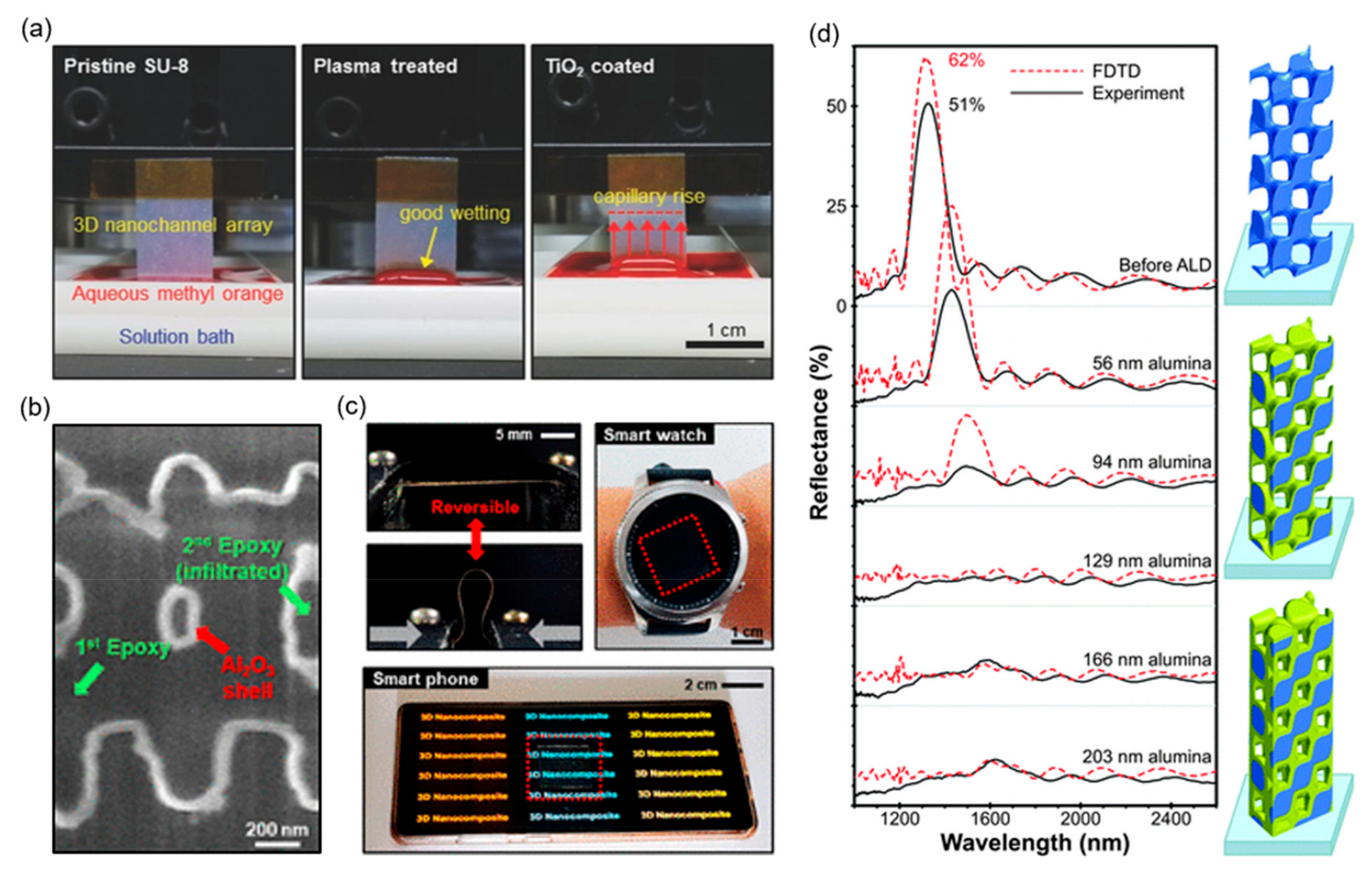
4.1. Organic–Inorganic Hybrid Nanocomposites

The resulting material produced through polymer template-assisted ALD is a structured composite with a polymer core and an inorganic shell deposited through ALD. In this case, the inorganic shell may serve to alter the surface properties of the original polymer template, or to complement its mechanical or optical properties.
A representative example of the former can be found in nanofluidic devices. Park et al. reported that a polymer template with densely packed, inch-length horizontal nanochannels possessing a diameter of 200 nm and a period of 400 nm was fabricated by performing PnP near the diffraction limit [23]. The template material was epoxy-based SU-8, with a hydrophobic surface. To utilize this unique nanochannel array as a nanofluidic filter for water treatment, it is necessary to change its surface to hydrophilic. However, it is very challenging to coat inch-length high-aspect-ratio pores of 200 nm diameter with a hydrophilic material uniformly. In this study, the authors successfully converted the nanochannels from hydrophobic to hydrophilic by conformally coating the TiO2 thin film through a thermal ALD process with a long supply time of precursors and reactants (Figure 6a). As the number of ALD cycles increased, a reduction in the size of the nanochannel was also observed. This TiO2-coated polymer nanochannel array was integrated into a microfluidic device and used as a high-throughput device that can stretch DNA or filter out sub-100-nm nanoparticles.
An example of modulating material properties through polymer template-assisted ALD can be found in interpenetrating network composites. Recently, Ahn et al. developed a new type of 3D continuous ceramic nanofiller-inserted polymer composite by filling an index-matched polymer in an Al2O3-coated 3D polymer nanonetwork prepared through the combination of PnP and ALD (Figure 6b) [26]. The content of the ceramic nanofiller, relative to the polymer matrix, can be finely controlled through the ALD cycle. Unlike conventional discrete ceramic nanoparticle–polymer composites, continuous interpenetrating network composites enable high loading above 15 vol%, owing to the absence of an aggregation of nanoparticles. The resulting composite film with a thickness of ~11 μm is not only optically transparent (>85% at 600 nm), but also mechanically flexible, because it has a structure in which the 3D nanostructured ultrathin (~60 nm) Al2O3 layer is embedded in the polymer matrix. The film can withstand bending strain without fracture, and can recover its original shape after relaxation. In addition, the continuous Al2O3 nanonetwork in the composite film provides an efficient heat transfer path for rapid heating and cooling. Thus, this composite can be used as a mechanically reinforced multifunctional optical film (Figure 6c). The ability to tune the material properties of the conformal inorganic thin films deposited by ALD is not limited to their mechanical properties but also to their optical properties, such as the photonic bandgap of photonic crystals (Figure 6d) [14,18].

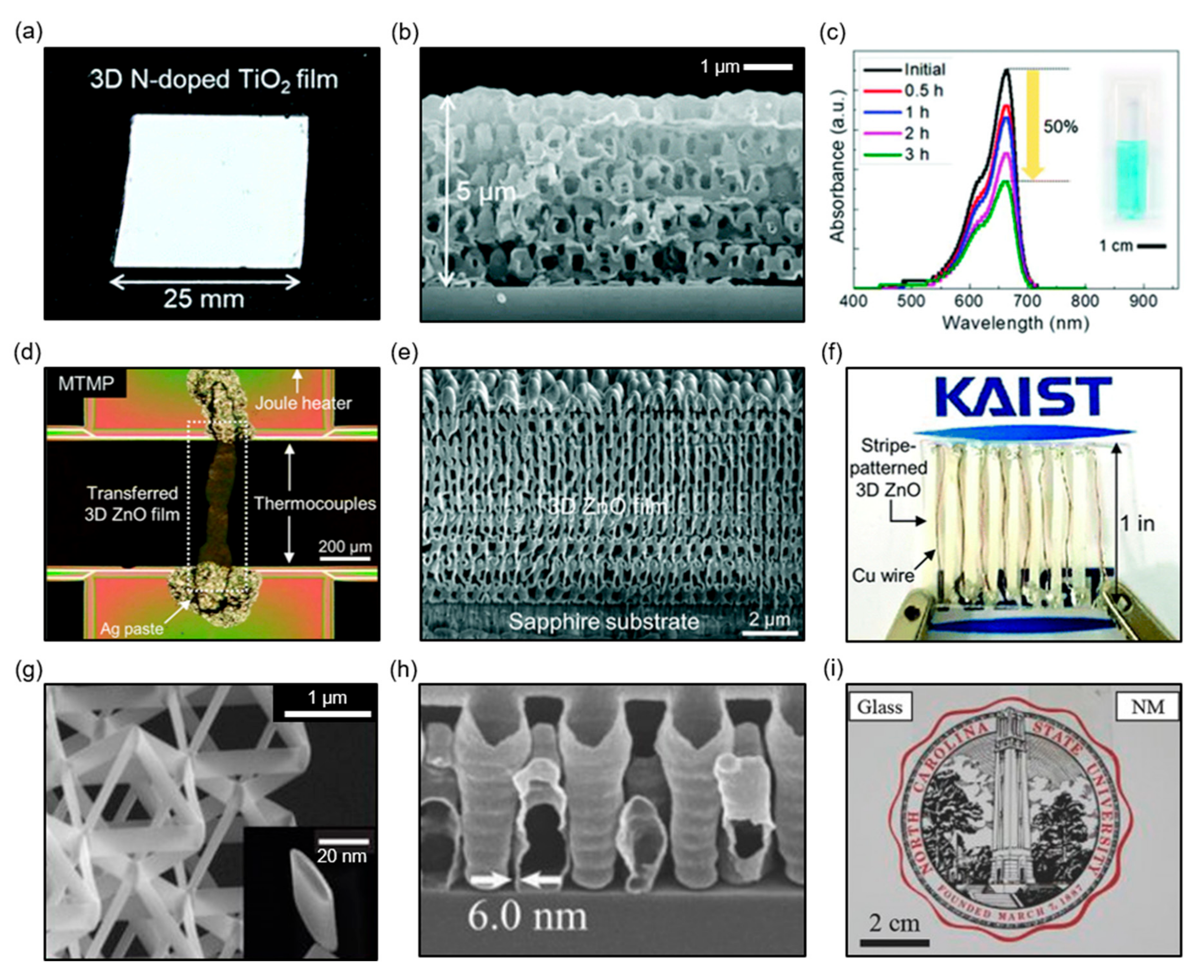
4.2. Highly Porous Hollow Inorganics

If the original polymer template is removed through calcination or an O2 plasma etching process, a highly porous inorganic material with a hollow 3D nanonetwork structure can be obtained. The hollow structure is very suitable for applications such as photocatalysts, which require a high surface area owing to surface reaction. Recently, a series of studies have reported on the fabrication of a periodic 3D nanonetwork monolith made of pure TiO2 or N-doped TiO2 through the combination of PnP and ALD, which is applied as a reusable photocatalytic film [21,22]. In the case of pure TiO2, amorphous TiO2 was deposited on the polymer template through thermal ALD at room temperature, which subsequently changed to anatase-phase TiO2 with excellent photocatalytic efficiency in the calcination process to remove the template. For N-doped TiO2 with enhanced visible light activity, an ultrathin (~10 nm) TiN layer was additionally deposited on the 3D hollow TiO2 nanonetwork through ALD at 350 °C. The TiN layer is then converted to an N-doped TiO2 layer by subsequent annealing at 550 °C in an atmospheric environment (Figure 7a–c). These monolithic films can be reused at least five times while maintaining good photocatalytic performance comparable to commercial TiO2 nanoparticles (P25).
One of the recently emerged applications of hollow inorganic nanonetworks is nanostructured thermoelectric materials [93,94,95,96,97]. A thermoelectric material is defined as a material with the ability to create a current or electric potential generated by a temperature difference between the two ends of the material, called the Seebeck effect. Thermoelectric devices have recently been reilluminated as a wearable energy-harvesting system because they can generate a weak current from the temperature difference between humans and their surroundings [98,99,100]. A representative approach for increasing the dimensionless figure-of-merit (ZT), which represents the performance of a thermoelectric material, is to reduce the thermal conductivity selectively while maintaining the Seebeck coefficient and electrical conductivity. This can be achieved by structuring the thermoelectric material into a hollow 3D nanonetwork. Kim et al. reported a nanostructured ZnO monolith with a low thermal conductivity (~3.6 W m−1 K−1 at 333 K), which is approximately 1/10 of that of the bulk ZnO through periodic 3D hollow nanostructuring of ZnO (Figure 7d–f) [27]. The lowering of the thermal conductivity comes from the enhancement of the phonon boundary scattering, while maintaining the electrical conductivity through the continuous nanonetwork structure. Although bulk pure ZnO cannot be used as a thermoelectric device, owing to its negligible ZT at room temperature, Kim et al. succeeded in fabricating the nanostructured ZnO-based thermoelectric device, producing 60 mV at a temperature difference of about 40 K.
Optical and mechanical metamaterials are receiving great attention in academia today. Metamaterials exhibit superior or new properties over conventional materials through artificially ordered structures of various scales. Several hollow 3D nanonetwork structures are optimized to implement these metamaterials. Meza et al. reported a hollow 3D ceramic nanonetwork designed to stretch a beam rather than bend it [16]. The key parameter of nanonetwork design is the ratio of wall thickness to beam radius, and if this ratio is small enough, the beam does not break by compression. Based on this structural design principle, they succeeded in producing a resilient Al2O3-based metamaterial with a hollow 3D nanonetwork structure through the combination of DLW and ALD. While common ceramics are very brittle and fragile, the developed mechanical metamaterial surprisingly recovered its original shape after more than 50% compression. Similarly, a mechanical metamaterial made of TiN converted from a polymer template, designed and produced through DLW, was also reported (Figure 7g) [15]. Most recently, to produce more practical-sized mechanical metamaterials, PnP optimized for large-area 3D nanofabrication was combined with this strategy to develop an inch-scale Al2O3-based mechanical metamaterial [25]. In addition to these unnatural mechanical properties, hollow 3D nanonetwork structures can also be applied to realize exceptional optical properties. For example, when forming a hollow 3D nanonetwork with an ultrathin (<5 nm) Al2O3 film through polymer template-assisted ALD and subsequent template removal, the refractive index of the material is theoretically lowered to 1.025, owing to the extremely small volume ratio (Figure 7h,i) [28,29]. This means that the resulting ceramic film is unnaturally transparent. By combining the above-mentioned novel mechanical and optical properties resulting from hollow 3D nanonetwork materials, a new level of multifunctional optical films can be achieved.

5. Summary and Outlook

In this review, we focused on the experimental realization and application of functional 3D nanonetworks based on polymer template-assisted ALD. Previous studies have shown that ALD and 3D polymer nanonetwork templates have excellent compatibility. Particularly, as the pore size gradually decreases to the submicron level, ALD is a unique technique that can uniformly coat the surface without clogging the pores. However, the extremely low GPC values of conventional ALD are not suitable for mass-production. In this regard, it is worth attempting to apply the recently proposed spatial ALD (SALD), which allows a much faster deposition rate, to complex nanostructures [101,102,103]. The remaining technical issue is to ensure the deposition of inorganic thin films at low temperatures. It is preferable to deposit a high-quality thin film at room temperature, considering the heat resistance of the polymer. In this regard, the potential of PEALD, which is capable of depositing a variety of high-quality thin films at lower temperatures than thermal ALD as a result of the presence of highly reactive ions and radicals, is very high. However, with the exception of a very few cases, most of the studies related to polymer template-assisted ALD reported so far depend on thermal ALD. This suggests that we should pay more attention to PEALD in the future to implement more useful and functional 3D nanonetworks. In particular, PEALD can deposit noble metals such as Pt at temperatures below 200 °C, which is difficult to achieve by thermal activation alone. By combining this capability with a nanoporous network structure, high-performance catalysts can be realized, which are very important in today’s energy and environmental communities. In summary, continuous efforts to combine ALD with actively evolving advanced nanofabrication techniques will provide opportunities for new levels of materials with exceptional properties.

Funding

This work was supported by the Low-dimensional Materials Genome Development funded by the Korea Research Institute of Standards and Science (KRISS-2018-18011084).

Conflicts of Interest

The authors declare no conflict of interest.

References

  1. George, S.M. Atomic Layer Deposition: An Overview. Chem. Rev. 2010, 110, 111–131. [Google Scholar] [CrossRef]
  2. Ritala, M.; Leskela, M. Handbook of thin film materials. Depos. Process. Thin Film 2002, 1, 103. [Google Scholar]
  3. Puurunen, R.L. Surface chemistry of atomic layer deposition: A case study for the trimethylaluminum/water process. J. Appl. Phys. 2005, 97, 121301. [Google Scholar] [CrossRef]
  4. Hwang, C.S. Atomic Layer Deposition for Semiconductors; Springer: Berlin, Germany, 2013. [Google Scholar]
  5. Kim, H. Atomic layer deposition of metal and nitride thin films: Current research efforts and applications for semiconductor device processing. J. Vac. Sci. Technol. B Microelectron. Nanometer Struct. 2003, 21, 2231–2261. [Google Scholar] [CrossRef]
  6. Groner, M.D.; Fabreguette, F.H.; Elam, J.W.; George, S.M. Low-Temperature Al2O3 Atomic Layer Deposition. Chem. Mater. 2004, 16, 639–645. [Google Scholar] [CrossRef]
  7. Knez, M.; Nielsch, K.; Niinistö, L. Synthesis and Surface Engineering of Complex Nanostructures by Atomic Layer Deposition. Adv. Mater. 2007, 19, 3425–3438. [Google Scholar] [CrossRef] [Green Version]
  8. Kim, E.; Vaynzof, Y.; Sepe, A.; Guldin, S.; Scherer, M.; Cunha, P.; Roth, S.V.; Steiner, U. Gyroid-Structured 3D ZnO Networks Made by Atomic Layer Deposition. Adv. Funct. Mater. 2014, 24, 863–872. [Google Scholar] [CrossRef]
  9. Ma, W.-C.; Huang, W.-S.; Ku, C.-S.; Ho, R.-M. Nanoporous gyroid metal oxides with controlled thickness and composition by atomic layer deposition from block copolymer templates. J. Mater. Chem. C 2016, 4, 840–849. [Google Scholar] [CrossRef]
  10. Werner, J.G.; Scherer, M.R.J.; Steiner, U.; Wiesner, U. Gyroidal mesoporous multifunctional nanocomposites via atomic layer deposition. Nanoscale 2014, 6, 8736–8742. [Google Scholar] [CrossRef]
  11. Li, F.; Yao, X.; Wang, Z.; Xing, W.; Jin, W.; Huang, J.; Wang, Y. Highly Porous Metal Oxide Networks of Interconnected Nanotubes by Atomic Layer Deposition. Nano Lett. 2012, 12, 5033–5038. [Google Scholar] [CrossRef]
  12. Guo, L.; Zhong, Z.; Wang, Y. Atomic Layer Deposition on Block Copolymer Membranes with Gyroidal Nanopores Toward Periodically Nanostructured Vapor Sensors: Nanotubes versus Nanorods. Adv. Mater. Interfaces 2016, 3, 1600017. [Google Scholar] [CrossRef]
  13. Peng, S.; Zhang, R.; Chen, V.H.; Khabiboulline, E.T.; Braun, P.; Atwater, H.A. Three-Dimensional Single Gyroid Photonic Crystals with a Mid-Infrared Bandgap. ACS Photonics 2016, 3, 1131–1137. [Google Scholar] [CrossRef] [Green Version]
  14. Frölich, A.; Wegener, M. Spectroscopic characterization of highly doped ZnO films grown by atomic-layer deposition for three-dimensional infrared metamaterials [Invited]. Opt. Mater. Express 2011, 1, 883–889. [Google Scholar] [CrossRef]
  15. Jang, D.; Meza, L.R.; Greer, F.; Greer, J.R. Fabrication and deformation of three-dimensional hollow ceramic nanostructures. Nat. Mater. 2013, 12, 893–898. [Google Scholar] [CrossRef] [PubMed] [Green Version]
  16. Meza, L.R.; Das, S.; Greer, J.R. Strong, lightweight, and recoverable three-dimensional ceramic nanolattices. Science 2014, 345, 1322–1326. [Google Scholar] [CrossRef] [PubMed] [Green Version]
  17. Kawata, S.; Sun, H.-B.; Tanaka, T.; Takada, K. Finer features for functional microdevices. Nature 2001, 412, 697–698. [Google Scholar] [CrossRef]
  18. Brzezinski, A.; Chen, Y.-C.; Wiltzius, P.; Braun, P.V. Complex three-dimensional conformal surfaces formed by atomic layer deposition: Computation and experimental verification. J. Mater. Chem. 2009, 19, 9126–9130. [Google Scholar] [CrossRef]
  19. Ramanan, V.; Nelson, E.; Brzezinski, A.; Braun, P.V.; Wiltzius, P. Three dimensional silicon-air photonic crystals with controlled defects using interference lithography. Appl. Phys. Lett. 2008, 92, 173304. [Google Scholar] [CrossRef]
  20. King, J.S.; Graugnard, E.; Roche, O.M.; Sharp, D.N.; Scrimgeour, J.; Denning, R.G.; Turberfield, A.J.; Summers, C.J. Infiltration and Inversion of Holographically Defined Polymer Photonic Crystal Templates by Atomic Layer Deposition. Adv. Mater. 2006, 18, 1561–1565. [Google Scholar] [CrossRef]
  21. Ahn, C.; Park, J.; Kim, D.; Jeon, S. Monolithic 3D titania with ultrathin nanoshell structures for enhanced photocatalytic activity and recyclability. Nanoscale 2013, 5, 10384–10389. [Google Scholar] [CrossRef]
  22. Cho, S.; Ahn, C.; Park, J.; Jeon, S. 3D nanostructured N-doped TiO2 photocatalysts with enhanced visible absorption. Nanoscale 2018, 10, 9747–9751. [Google Scholar] [CrossRef] [PubMed]
  23. Park, J.; Kim, K.-I.; Kim, K.; Kim, D.-C.; Cho, D.; Lee, J.H.; Jeon, S. Rapid, High-Resolution 3D Interference Printing of Multilevel Ultralong Nanochannel Arrays for High-Throughput Nanofluidic Transport. Adv. Mater. 2015, 27, 8000–8006. [Google Scholar] [CrossRef]
  24. Bong, J.; Ahn, C.; Lim, T.; Park, J.H.; Kwak, S.K.; Jeon, S.; Ju, S. Controlled three-dimensional interconnected capillary structures for liquid repellency engineering. RSC Adv. 2016, 6, 61909–61914. [Google Scholar] [CrossRef]
  25. Na, Y.-E.; Shin, D.; Kim, K.; Ahn, C.; Jeon, S.; Jang, D. Emergence of New Density–Strength Scaling Law in 3D Hollow Ceramic Nanoarchitectures. Small 2018, 14, 1802239. [Google Scholar] [CrossRef]
  26. Ahn, C.; Kim, S.-M.; Jung, J.-W.; Park, J.; Kim, T.; Lee, S.E.; Jang, D.; Hong, J.-W.; Han, S.M.; Jeon, S. Multifunctional Polymer Nanocomposites Reinforced by 3D Continuous Ceramic Nanofillers. ACS Nano 2018, 12, 9126–9133. [Google Scholar] [CrossRef] [PubMed]
  27. Kim, K.; Park, J.; Hong, S.; Park, S.H.; Jeon, S.G.; Ahn, C.; Song, J.Y.; Jeon, S. Anomalous thermoelectricity of pure ZnO from 3D continuous ultrathin nanoshell structures. Nanoscale 2018, 10, 3046–3052. [Google Scholar] [CrossRef]
  28. Bagal, A.; Zhang, X.A.; Shahrin, R.; Dandley, E.C.; Zhao, J.; Poblete, F.R.; Oldham, C.J.; Zhu, Y.; Parsons, G.N.; Bobko, C.; et al. Large-Area Nanolattice Film with Enhanced Modulus, Hardness, and Energy Dissipation. Sci. Rep. 2017, 7, 9145. [Google Scholar] [CrossRef] [Green Version]
  29. Zhang, X.A.; Bagal, A.; Dandley, E.C.; Zhao, J.; Oldham, C.J.; Wu, B.-I.; Parsons, G.N.; Chang, C.-H. Ordered 3D Thin-Shell Nanolattice Materials with Near-Unity Refractive Indices. Adv. Funct. Mater. 2015, 25, 6644–6649. [Google Scholar] [CrossRef]
  30. Lee, K.; Yoon, H.; Ahn, C.; Park, J.; Jeon, S. Strategies to improve the photocatalytic activity of TiO2: 3D nanostructuring and heterostructuring with graphitic carbon nanomaterials. Nanoscale 2019, 11, 7025–7040. [Google Scholar] [CrossRef]
  31. Moon, J.H.; Yang, S. Chemical Aspects of Three-Dimensional Photonic Crystals. Chem. Rev. 2010, 110, 547–574. [Google Scholar] [CrossRef] [PubMed]
  32. Kashani, H.; Ito, Y.; Han, J.; Liu, P.; Chen, M. Extraordinary tensile strength and ductility of scalable nanoporous graphene. Sci. Adv. 2019, 5, eaat6951. [Google Scholar] [CrossRef]
  33. Park, S.-G.; Jeon, T.Y.; Jeon, H.C.; Yang, S.-M.; Kwon, J.-D.; Mun, C.-W.; Cho, B.; Kim, C.S.; Kim, D.-H. Fabrication of 3D ZnO hollow shell structures by prism holographic lithography and atomic layer deposition. J. Mater. Chem. C 2014, 2, 1957–1961. [Google Scholar] [CrossRef]
  34. Campo, A.D.; Greiner, C. SU-8: A photoresist for high-aspect-ratio and 3D submicron lithography. J. Micromech. Microeng. 2007, 17, R81–R95. [Google Scholar] [CrossRef]
  35. Hsueh, H.-Y.; Yao, C.-T.; Ho, R.-M. Well-ordered nanohybrids and nanoporous materials from gyroid block copolymer templates. Chem. Soc. Rev. 2015, 44, 1974–2018. [Google Scholar] [CrossRef]
  36. Peng, Q.; Sun, X.-Y.; Spagnola, J.C.; Hyde, G.K.; Spontak, R.J.; Parsons, G.N. Atomic Layer Deposition on Electrospun Polymer Fibers as a Direct Route to Al2O3 Microtubes with Precise Wall Thickness Control. Nano Lett. 2007, 7, 719–722. [Google Scholar] [CrossRef]
  37. Jeon, S.; Park, J.-U.; Cirelli, R.; Yang, S.; Heitzman, C.E.; Braun, P.V.; Kenis, P.J.A.; Rogers, J.A. Fabricating complex three-dimensional nanostructures with high-resolution conformable phase masks. Proc. Natl. Acad. Sci. USA 2004, 101, 12428–12433. [Google Scholar] [CrossRef] [PubMed] [Green Version]
  38. Greiner, A.; Wendorff, J.H. Electrospinning: A Fascinating Method for the Preparation of Ultrathin Fibers. Angew. Chem. Int. Ed. 2007, 46, 5670–5703. [Google Scholar] [CrossRef]
  39. Kim, I.-D. Advances in Electrospun Functional Nanofibers. Macromol. Mater. Eng. 2013, 298, 473–474. [Google Scholar] [CrossRef] [Green Version]
  40. Huang, Z.-M.; Zhang, Y.Z.; Kotaki, M.; Ramakrishna, S. A review on polymer nanofibers by electrospinning and their applications in nanocomposites. Compos. Sci. Technol. 2003, 63, 2223–2253. [Google Scholar] [CrossRef]
  41. Yuan, H.; Zhou, Q.; Zhang, Y. 6—Improving fiber alignment during electrospinning. In Electrospun Nanofibers; Afshari, M., Ed.; Woodhead Publishing: Sawston, UK, 2017; pp. 125–147. [Google Scholar] [CrossRef]
  42. Ross, C.A.; Berggren, K.K.; Cheng, J.Y.; Jung, Y.S.; Chang, J.-B. Three-Dimensional Nanofabrication by Block Copolymer Self-Assembly. Adv. Mater. 2014, 26, 4386–4396. [Google Scholar] [CrossRef] [PubMed]
  43. Hsueh, H.-Y.; Chen, H.-Y.; She, M.-S.; Chen, C.-K.; Ho, R.-M.; Gwo, S.; Hasegawa, H.; Thomas, E.L. Inorganic Gyroid with Exceptionally Low Refractive Index from Block Copolymer Templating. Nano Lett. 2010, 10, 4994–5000. [Google Scholar] [CrossRef] [PubMed]
  44. Deubel, M.; von Freymann, G.; Wegener, M.; Pereira, S.; Busch, K.; Soukoulis, C.M. Direct laser writing of three-dimensional photonic-crystal templates for telecommunications. Nat. Mater. 2004, 3, 444. [Google Scholar] [CrossRef] [PubMed]
  45. Deng, Y.; Wei, J.; Sun, Z.; Zhao, D. Large-pore ordered mesoporous materials templated from non-Pluronic amphiphilic block copolymers. Chem. Soc. Rev. 2013, 42, 4054–4070. [Google Scholar] [CrossRef] [PubMed]
  46. Beckmann, D.; Schnitzler, D.; Schaefer, D.; Gottmann, J.; Kelbassa, I. Beam shaping of laser diode radiation by waveguides with arbitrary cladding geometry written with fs-laser radiation. Opt. Express 2011, 19, 25418–25425. [Google Scholar] [CrossRef] [PubMed]
  47. Stankevičius, E.; Daugnoraitė, E.; Račiukaitis, G. Mechanism of pillars formation using four-beam interference lithography. Opt. Lasers Eng. 2019, 116, 41–46. [Google Scholar] [CrossRef]
  48. Jeon, S.; Malyarchuk, V.; Rogers, J.A.; Wiederrecht, G.P. Fabricating three dimensional nanostructures using two photon lithography in a single exposure step. Opt. Express 2006, 14, 2300–2308. [Google Scholar] [CrossRef] [PubMed]
  49. Campbell, M.; Sharp, D.N.; Harrison, M.T.; Denning, R.G.; Turberfield, A.J. Fabrication of photonic crystals for the visible spectrum by holographic lithography. Nature 2000, 404, 53–56. [Google Scholar] [CrossRef]
  50. Kondo, T.; Juodkazis, S.; Mizeikis, V.; Misawa, H.; Matsuo, S. Holographic lithography of periodic two-and three-dimensional microstructures in photoresist SU-8. Opt. Express 2006, 14, 7943–7953. [Google Scholar] [CrossRef]
  51. Jeon, T.; Kim, D.-H.; Park, S.-G. Holographic Fabrication of 3D Nanostructures. Adv. Mater. Interfaces 2018, 5, 1800330. [Google Scholar] [CrossRef]
  52. Ullal, C.K.; Maldovan, M.; Thomas, E.L.; Chen, G.; Han, Y.-J.; Yang, S. Photonic crystals through holographic lithography: Simple cubic, diamond-like, and gyroid-like structures. Appl. Phys. Lett. 2004, 84, 5434–5436. [Google Scholar] [CrossRef]
  53. Park, J.; Wang, S.; Li, M.; Ahn, C.; Hyun, J.K.; Kim, D.S.; Kim, D.K.; Rogers, J.A.; Huang, Y.; Jeon, S. Three-dimensional nanonetworks for giant stretchability in dielectrics and conductors. Nat. Commun. 2012, 3, 916. [Google Scholar] [CrossRef] [PubMed] [Green Version]
  54. Park, J.; Park, J.H.; Kim, E.; Ahn, C.W.; Jang, H.I.; Rogers, J.A.; Jeon, S. Conformable Solid-Index Phase Masks Composed of High-Aspect-Ratio Micropillar Arrays and Their Application to 3D Nanopatterning. Adv. Mater. 2011, 23, 860–864. [Google Scholar] [CrossRef] [PubMed]
  55. Park, J.; Yoon, S.; Kang, K.; Jeon, S. Antireflection Behavior of Multidimensional Nanostructures Patterned Using a Conformable Elastomeric Phase Mask in a Single Exposure Step. Small 2010, 6, 1981–1985. [Google Scholar] [CrossRef] [PubMed]
  56. Park, J.; Seo, J.; Jung, H.K.; Hyun, G.; Park, S.Y.; Jeon, S. Direct Optical Fabrication of Fluorescent, Multilevel 3D Nanostructures for Highly Efficient Chemosensing Platforms. Adv. Funct. Mater. 2016, 26, 7170–7177. [Google Scholar] [CrossRef]
  57. Shir, D.J.; Jeon, S.; Liao, H.; Highland, M.; Cahill, D.G.; Su, M.F.; El-Kady, I.F.; Christodoulou, C.G.; Bogart, G.R.; Hamza, A.V.; et al. Three-Dimensional Nanofabrication with Elastomeric Phase Masks. J. Phys. Chem. B 2007, 111, 12945–12958. [Google Scholar] [CrossRef]
  58. Park, J.; Tahk, D.; Ahn, C.; Im, S.G.; Choi, S.-J.; Suh, K.-Y.; Jeon, S. Conformal phase masks made of polyurethane acrylate with optimized elastic modulus for 3D nanopatterning. J. Mater. Chem. C 2014, 2, 2316–2322. [Google Scholar] [CrossRef]
  59. Hyun, J.K.; Park, J.; Kim, E.; Lauhon, L.J.; Jeon, S. Rational Control of Diffraction and Interference from Conformal Phase Gratings: Toward High-Resolution 3D Nanopatterning. Adv. Opt. Mater. 2014, 2, 1213–1220. [Google Scholar] [CrossRef]
  60. Rinne, J.W.; Wiltzius, P. Design of holographic structures using genetic algorithms. Opt. Express 2006, 14, 9909–9916. [Google Scholar] [CrossRef] [PubMed]
  61. Rinne, J.W.; Gupta, S.; Wiltzius, P. Inverse design for phase mask lithography. Opt. Express 2008, 16, 663–670. [Google Scholar] [CrossRef] [PubMed]
  62. SalehHudin, H.S.; Mohamad, E.N.; Mahadi, W.N.L.; Muhammad Afifi, A. Multiple-jet electrospinning methods for nanofiber processing: A review. Mater. Manuf. Process. 2018, 33, 479–498. [Google Scholar] [CrossRef]
  63. Chen, L.; Wang, S.; Yu, Q.; Topham, P.D.; Chen, C.; Wang, L. A comprehensive review of electrospinning block copolymers. Soft Matter 2019. [Google Scholar] [CrossRef]
  64. Khalf, A.; Madihally, S.V. Recent advances in multiaxial electrospinning for drug delivery. Eur. J. Pharm. Biopharm. 2017, 112, 1–17. [Google Scholar] [CrossRef] [PubMed]
  65. Woo, S.; Wang, H.S.; Choe, Y.; Huh, J.; Bang, J. Three-Dimensional Multilayered Nanostructures from Crosslinkable Block Copolymers. ACS Macro Lett. 2016, 5, 287–291. [Google Scholar] [CrossRef]
  66. Feng, H.; Lu, X.; Wang, W.; Kang, N.-G.; Mays, J.W. Block Copolymers: Synthesis, Self-Assembly, and Applications. Polymers 2017, 9, 494. [Google Scholar] [CrossRef] [PubMed]
  67. Feng, X.; Guo, H.; Thomas, E.L. Topological defects in tubular network block copolymers. Polymer 2019, 168, 44–52. [Google Scholar] [CrossRef]
  68. Kwon, Y.W.; Park, J.; Kim, T.; Kang, S.H.; Kim, H.; Shin, J.; Jeon, S.; Hong, S.W. Flexible Near-Field Nanopatterning with Ultrathin, Conformal Phase Masks on Nonplanar Substrates for Biomimetic Hierarchical Photonic Structures. ACS Nano 2016, 10, 4609–4617. [Google Scholar] [CrossRef] [PubMed]
  69. Kayaci, F.; Vempati, S.; Ozgit-Akgun, C.; Biyikli, N.; Uyar, T. Enhanced photocatalytic activity of homoassembled ZnO nanostructures on electrospun polymeric nanofibers: A combination of atomic layer deposition and hydrothermal growth. Appl. Catal. B Environ. 2014, 156–157, 173–183. [Google Scholar] [CrossRef]
  70. Biener, M.M.; Ye, J.; Baumann, T.F.; Wang, Y.M.; Shin, S.J.; Biener, J.; Hamza, A.V. Ultra-strong and Low-Density Nanotubular Bulk Materials with Tunable Feature Sizes. Adv. Mater. 2014, 26, 4808–4813. [Google Scholar] [CrossRef] [PubMed]
  71. Kayaci, F.; Ozgit-Akgun, C.; Donmez, I.; Biyikli, N.; Uyar, T. Polymer–Inorganic Core–Shell Nanofibers by Electrospinning and Atomic Layer Deposition: Flexible Nylon–ZnO Core–Shell Nanofiber Mats and Their Photocatalytic Activity. ACS Appl. Mater. Interfaces 2012, 4, 6185–6194. [Google Scholar] [CrossRef] [PubMed] [Green Version]
  72. Elam, J.W.; Routkevitch, D.; Mardilovich, P.P.; George, S.M. Conformal Coating on Ultrahigh-Aspect-Ratio Nanopores of Anodic Alumina by Atomic Layer Deposition. Chem. Mater. 2003, 15, 3507–3517. [Google Scholar] [CrossRef]
  73. Wilson, C.A.; Grubbs, R.K.; George, S.M. Nucleation and Growth during Al2O3 Atomic Layer Deposition on Polymers. Chem. Mater. 2005, 17, 5625–5634. [Google Scholar] [CrossRef]
  74. Guo, H.C.; Ye, E.; Li, Z.; Han, M.-Y.; Loh, X.J. Recent progress of atomic layer deposition on polymeric materials. Mater. Sci. Eng. C 2017, 70, 1182–1191. [Google Scholar] [CrossRef] [PubMed]
  75. Parsons, G.N.; Atanasov, S.E.; Dandley, E.C.; Devine, C.K.; Gong, B.; Jur, J.S.; Lee, K.; Oldham, C.J.; Peng, Q.; Spagnola, J.C.; et al. Mechanisms and reactions during atomic layer deposition on polymers. Coord. Chem. Rev. 2013, 257, 3323–3331. [Google Scholar] [CrossRef]
  76. Brozena, A.H.; Oldham, C.J.; Parsons, G.N. Atomic layer deposition on polymer fibers and fabrics for multifunctional and electronic textiles. J. Vac. Sci. Technol. A 2016, 34, 010801. [Google Scholar] [CrossRef]
  77. Haider, A.; Yilmaz, M.; Deminskyi, P.; Eren, H.; Biyikli, N. Nanoscale selective area atomic layer deposition of TiO2 using e-beam patterned polymers. RSC Adv. 2016, 6, 106109–106119. [Google Scholar] [CrossRef]
  78. Sinha, A.; Hess, D.W.; Henderson, C.L. Area selective atomic layer deposition of titanium dioxide: Effect of precursor chemistry. J. Vac. Sci. Technol. B Microelectron. Nanometer Struct. 2006, 24, 2523–2532. [Google Scholar] [CrossRef]
  79. Färm, E.; Kemell, M.; Ritala, M.; Leskelä, M. Selective-Area Atomic Layer Deposition Using Poly(methyl methacrylate) Films as Mask Layers. J. Phys. Chem. C 2008, 112, 15791–15795. [Google Scholar] [CrossRef]
  80. Chen, R.; Bent, S.F. Chemistry for Positive Pattern Transfer Using Area-Selective Atomic Layer Deposition. Adv. Mater. 2006, 18, 1086–1090. [Google Scholar] [CrossRef]
  81. Seo, S.; Yeo, B.C.; Han, S.S.; Yoon, C.M.; Yang, J.Y.; Yoon, J.; Yoo, C.; Kim, H.-J.; Lee, Y.-B.; Lee, S.J.; et al. Reaction Mechanism of Area-Selective Atomic Layer Deposition for Al2O3 Nanopatterns. ACS Appl. Mater. Interfaces 2017, 9, 41607–41617. [Google Scholar] [CrossRef] [PubMed]
  82. Leng, C.Z.; Losego, M.D. Vapor phase infiltration (VPI) for transforming polymers into organic–inorganic hybrid materials: A critical review of current progress and future challenges. Mater. Horiz. 2017, 4, 747–771. [Google Scholar] [CrossRef]
  83. Lee, S.-M.; Pippel, E.; Gösele, U.; Dresbach, C.; Qin, Y.; Chandran, C.V.; Bräuniger, T.; Hause, G.; Knez, M. Greatly Increased Toughness of Infiltrated Spider Silk. Science 2009, 324, 488–492. [Google Scholar] [CrossRef] [PubMed]
  84. Xie, W.; Khan, S.; Rojas, O.J.; Parsons, G.N. Control of Micro- and Mesopores in Carbon Nanofibers and Hollow Carbon Nanofibers Derived from Cellulose Diacetate via Vapor Phase Infiltration of Diethyl Zinc. ACS Sustain. Chem. Eng. 2018, 6, 13844–13853. [Google Scholar] [CrossRef]
  85. Mackus, A.J.M.; Garcia-Alonso, D.; Knoops, H.C.M.; Bol, A.A.; Kessels, W.M.M. Room-Temperature Atomic Layer Deposition of Platinum. Chem. Mater. 2013, 25, 1769–1774. [Google Scholar] [CrossRef]
  86. Ozgit-Akgun, C.; Kayaci, F.; Donmez, I.; Uyar, T.; Biyikli, N. Template-Based Synthesis of Aluminum Nitride Hollow Nanofibers Via Plasma-Enhanced Atomic Layer Deposition. J. Am. Ceram. Soc. 2013, 96, 916–922. [Google Scholar] [CrossRef]
  87. Ozgit-Akgun, C.; Kayaci, F.; Vempati, S.; Haider, A.; Celebioglu, A.; Goldenberg, E.; Kizir, S.; Uyar, T.; Biyikli, N. Fabrication of flexible polymer–GaN core–shell nanofibers by the combination of electrospinning and hollow cathode plasma-assisted atomic layer deposition. J. Mater. Chem. C 2015, 3, 5199–5206. [Google Scholar] [CrossRef] [Green Version]
  88. Aaltonen, T.; Ritala, M.; Sajavaara, T.; Keinonen, J.; Leskelä, M. Atomic Layer Deposition of Platinum Thin Films. Chem. Mater. 2003, 15, 1924–1928. [Google Scholar] [CrossRef]
  89. Musschoot, J.; Dendooven, J.; Deduytsche, D.; Haemers, J.; Buyle, G.; Detavernier, C. Conformality of thermal and plasma enhanced atomic layer deposition on a non-woven fibrous substrate. Surf. Coat. Technol. 2012, 206, 4511–4517. [Google Scholar] [CrossRef]
  90. Ozgit-Akgun, C.; Goldenberg, E.; Bolat, S.; Tekcan, B.; Kayaci, F.; Uyar, T.; Okyay, A.K.; Biyikli, N. Low-temperature hollow cathode plasma-assisted atomic layer deposition of crystalline III-nitride thin films and nanostructures. Phys. Status Solidi C 2015, 12, 394–398. [Google Scholar] [CrossRef] [Green Version]
  91. Knoops, H.C.M.; Faraz, T.; Arts, K.; Kessels, W.M.M. Status and prospects of plasma-assisted atomic layer deposition. J. Vac. Sci. Technol. A 2019, 37, 030902. [Google Scholar] [CrossRef]
  92. Sweet, W.J.; Oldham, C.J.; Parsons, G.N. Atomic Layer Deposition of Metal Oxide Patterns on Nonwoven Fiber Mats using Localized Physical Compression. ACS Appl. Mater. Interfaces 2014, 6, 9280–9289. [Google Scholar] [CrossRef] [PubMed]
  93. Hong, S.; Park, J.; Jeon, S.G.; Kim, K.; Park, S.H.; Shin, H.S.; Kim, B.; Jeon, S.; Song, J.Y. Monolithic Bi1.5Sb0.5Te3 ternary alloys with a periodic 3D nanostructure for enhancing thermoelectric performance. J. Mater. Chem. C 2017, 5, 8974–8980. [Google Scholar] [CrossRef]
  94. Li, J.-F.; Liu, W.-S.; Zhao, L.-D.; Zhou, M. High-performance nanostructured thermoelectric materials. NPG Asia Mater. 2010, 2, 152. [Google Scholar] [CrossRef]
  95. Kim, S.I.; Lee, K.H.; Mun, H.A.; Kim, H.S.; Hwang, S.W.; Roh, J.W.; Yang, D.J.; Shin, W.H.; Li, X.S.; Lee, Y.H.; et al. Dense dislocation arrays embedded in grain boundaries for high-performance bulk thermoelectrics. Science 2015, 348, 109–114. [Google Scholar] [CrossRef] [Green Version]
  96. Minnich, A.J.; Dresselhaus, M.S.; Ren, Z.F.; Chen, G. Bulk nanostructured thermoelectric materials: Current research and future prospects. Energy Environ. Sci. 2009, 2, 466–479. [Google Scholar] [CrossRef]
  97. Shin, H.S.; Jeon, S.G.; Yu, J.; Kim, Y.-S.; Park, H.M.; Song, J.Y. Twin-driven thermoelectric figure-of-merit enhancement of Bi2Te3 nanowires. Nanoscale 2014, 6, 6158–6165. [Google Scholar] [CrossRef] [PubMed]
  98. Kim, S.J.; We, J.H.; Cho, B.J. A wearable thermoelectric generator fabricated on a glass fabric. Energy Environ. Sci. 2014, 7, 1959–1965. [Google Scholar] [CrossRef]
  99. Kim, M.-K.; Kim, M.-S.; Lee, S.; Kim, C.; Kim, Y.-J. Wearable thermoelectric generator for harvesting human body heat energy. Smart Mater. Struct. 2014, 23, 105002. [Google Scholar] [CrossRef]
  100. Bahk, J.-H.; Fang, H.; Yazawa, K.; Shakouri, A. Flexible thermoelectric materials and device optimization for wearable energy harvesting. J. Mater. Chem. C 2015, 3, 10362–10374. [Google Scholar] [CrossRef]
  101. Poodt, P.; Cameron, D.C.; Dickey, E.; George, S.M.; Kuznetsov, V.; Parsons, G.N.; Roozeboom, F.; Sundaram, G.; Vermeer, A. Spatial atomic layer deposition: A route towards further industrialization of atomic layer deposition. J. Vac. Sci. Technol. A 2012, 30, 010802. [Google Scholar] [CrossRef] [Green Version]
  102. Muñoz-Rojas, D.; Maindron, T.; Esteve, A.; Piallat, F.; Kools, J.C.S.; Decams, J.M. Speeding up the unique assets of atomic layer deposition. Mater. Today Chem. 2019, 12, 96–120. [Google Scholar] [CrossRef]
  103. Muñoz-Rojas, D.; Nguyen, V.H.; Masse de la Huerta, C.; Jiménez, C.; Bellet, D. Spatial Atomic Layer Deposition; InTech: Rijeka, Croatia, 2019. [Google Scholar]
Figure 1. Schematic representation of (a) one cycle of thermal atomic layer deposition (ALD) or plasma-enhanced ALD (PEALD), (b) the fabrication process of polymer–inorganic composite or hollow inorganic materials from a polymer template with irregular three-dimensional (3D) nanonetworks, and (c) the fabrication process of polymer–inorganic composite or hollow inorganic materials from a polymer template with regular 3D nanonetworks.
Applsci 09 01990 g001
Figure 2. Schematic representation of the fabrication methods of 3D nanonetwork-structured polymer templates: (a) electrospinning (reprinted with permission from [37]. Copyright 2004 John Wiley and Sons); (b) block-copolymer (BCP) lithography (reprinted with permission from [45]. Copyright 2013 The Royal Society of Chemistry); (c) direct laser writing (DLW) (reprinted with permission from [46]. Copyright 2011 The Optical Society (OSA)); (d) multibeam interference lithography (MBIL) (reprinted with permission from [47]. Copyright 2011 The Optical Society (OSA)); (e) proximity-field nanopatterning (PnP) (reprinted with permission from [48]. Copyright 2006 The Optical Society (OSA)).
Applsci 09 01990 g002
Figure 3. SEM images of polymer templates with irregular or regular 3D nanonetwork structures fabricated through 3D nanofabrication techniques: (a) electrospinning (reprinted with permission from [69]. Copyright 2014 Elsevier); (b) BCP lithography (reprinted with permission from [10]. Copyright 2014 The Royal Society of Chemistry); (c) DLW (reprinted with permission from [44]. Copyright 2004 Nature Materials); (d) MBIL (reprinted with permission from [18]. Copyright 2009 The Royal Society of Chemistry); (e) one-photon PnP; (f) two-photon PnP (reprinted with permission from [48]. Copyright 2006 The Optical Society (OSA)); (g) one-photon PnP with a binary phase-mask (reprinted with permission from [23]. Copyright 2015 John Wiley and Sons).
Applsci 09 01990 g003
Figure 4. Various inorganic thin films conformally deposited on 3D nanonetwork polymer templates through thermal ALD: (a) SEM image of a ZnO thin film deposited on a polymer template formed by electrospinning; (b) TEM image of (a) (reprinted with permission from [71]. Copyright 2012 American Chemical Society); (c) TEM image of Al2O3 and ZnO thin films deposited on a polymer template formed by BCP lithography (reprinted with permission from [9]. Copyright 2015 The Royal Society of Chemistry); (d) cross-sectional SEM image of an Al-doped ZnO thin film on a polymer template formed by DLW (reprinted with permission from [14]. Copyright 2011 The Optical Society (OSA)); (e) cross-sectional SEM image of an Al2O3 thin film deposited on a polymer template formed by MBIL (reprinted with permission from [18]. Copyright 2009 The Royal Society of Chemistry); (f) cross-sectional SEM image of an Al2O3 thin film deposited on a polymer template formed by PnP (reprinted with permission from [26]. Copyright 2018 American Chemical Society); (g) cross-sectional SEM and EDS images of a TiO2 thin film deposited on a polymer template formed by PnP (reprinted with permission from [21]. Copyright 2013 The Royal Society of Chemistry).
Applsci 09 01990 g004
Figure 5. Various inorganic thin films conformally deposited on 3D nanonetwork polymer templates through PEALD: (a) digital image of a Pt thin film deposited on a woven cotton fabric; (b) SEM image of (a); (c) elemental composition of (a) (reprinted with permission from [85]. Copyright 2013 American Chemical Society); (d) SEM image of an AlN thin film deposited on an electrospun 3D nanonetwork (reprinted with permission from [86]. Copyright 2012 John Wiley and Sons); (e) TEM image of a GaN thin film deposited on an electrospun 3D nanonetwork; (f) elemental composition of (e) (reprinted with permission from [87]. Copyright 2015 The Royal Society of Chemistry).
Applsci 09 01990 g005
Figure 6. Application of inorganic shell-polymer nanonetwork composites: (a) comparison of hydrophilicity before and after conformal coating of TiO2 thin film on ultralong nanochannel arrays formed by PnP (reprinted with permission from [23]. Copyright 2015 John Wiley and Sons); (b) cross-sectional SEM image of 3D continuous ceramic nanofiller-inserted polymer composite by filling an index-matched polymer in an Al2O3-coated 3D polymer nanonetwork; (c) digital images of transparent, flexible, and mechanically reinforced composite (reprinted with permission from [26]. Copyright 2018 American Chemical Society); (d) modulation of reflectance of 3D photonic crystals through Al2O3 thin film coating (reprinted with permission from [18]. Copyright 2009 The Royal Society of Chemistry).
Applsci 09 01990 g006
Figure 7. Application of highly porous inorganic materials with a hollow 3D nanonetwork structure: (a) digital image of a large-area (625 mm2), 3D nanonetwork-structured, N-doped TiO2 film produced by PnP and ALD; (b) cross-sectional SEM image of (a); (c) photocatalytic degradation of methylene blue solution under solar irradiation (reprinted with permission from [22]. Copyright 2018 The Royal Society of Chemistry); (d) optical microscope image of a 3D nanonetwork-structured ZnO film transferred on a microfabricated thermoelectric measurement platform (MTMP); (e) cross-sectional SEM image of (d); (f) digital image of a thermoelectric device prototype based on 3D nanonetwork-structured ZnO stripes (reprinted with permission from [27]. Copyright 2018 The Royal Society of Chemistry); (g) SEM image of an abnormally resilient 3D nanonetwork-structured TiN film produced by DLW and ALD (reprinted with permission from [15]. Copyright 2013 Nature Materials); (h) cross-sectional SEM image of a 3D nanonetwork-structured Al2O3 film with a thickness of 6 nm; (i) digital image of a highly transparent, 3D nanonetwork-structured Al2O3 film coated on a glass substrate (reprinted with permission from [29]. Copyright 2015 John Wiley and Sons).
Applsci 09 01990 g007
Table 1. The process parameters of selected cases of polymer template-assisted atomic layer deposition (ALD).
ALD TypeTemplate Preparation MethodTemplate
Structure Regularity
PrecursorReactant/Plasma GasTemperature (°C)Deposited
Materials
Ref.
ThermalElectrospinningIrregularDEZH2O200ZnO[69]
ThermalElectrospinningIrregularDEZH2O200ZnO[71]
ThermalNonwoven fabricIrregularDEZH2O125–155ZnO[92]
ThermalBCP lithographyRegularTiCl4H2O150TiO2[10]
ThermalBCP lithographyRegularDEZH2O50ZnO[9]
ThermalDLWRegularDEZ + TMAH2O250Al:ZnO[14]
ThermalDLWRegularDEZ + TIPH2O250Ti:ZnO[14]
ThermalMBILRegularTiCl4H2O100TiO2[20]
ThermalMBILRegularTMAH2O85Al2O3[18]
ThermalMBILRegularDEZH2O100ZnO[33]
ThermalPnPRegularTDMATH2O90TiO2[22]
ThermalPnPRegularTDMATNH3350TiN[22]
ThermalPnPRegularDEZH2O150ZnO[27]
Plasma-enhancedNonwoven fabricIrregularTMAO275Al2O3[89]
Plasma-enhancedElectrospinningIrregularTMANH3200AlN[86]
Plasma-enhancedElectrospinningIrregularGaMe3N2 / H2200GaN[87]
Plasma-enhancedWoven fabricIrregularMeCpPtMe3O2 / H2RTPt[85]
DEZ, diethylzinc; TMA, trimethylaluminum; TIP, titaniumisopropoxide; TDMAT, tetrakis-dimethyl-amino titanium; GaMe3, trimethylgallium.

