Charge Carrier Distribution in Low-Voltage Dual-Gate Organic Thin-Film Transistors

 , ,
, , 
Abstract
:Featured Application
Abstract
1. Introduction
2. Materials and Methods
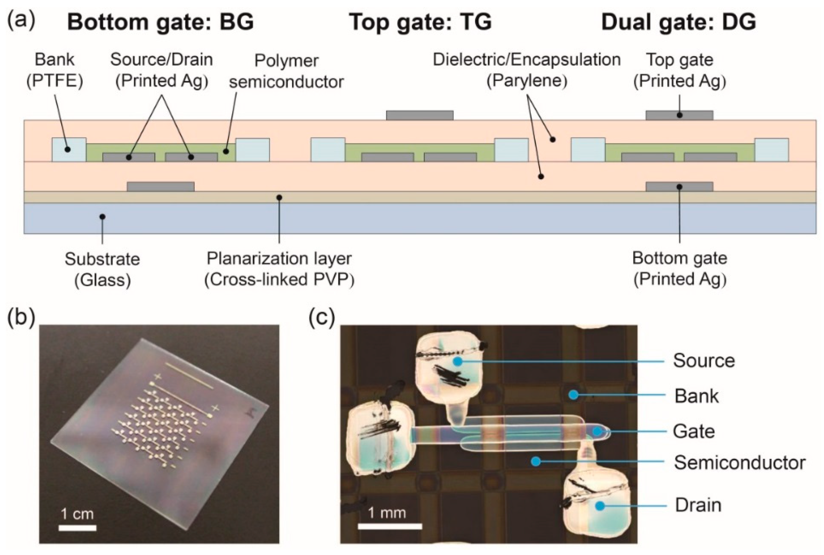
2.1. Device Fabrication
2.2. Device Characterization
2.3. Method of the Device Simulation
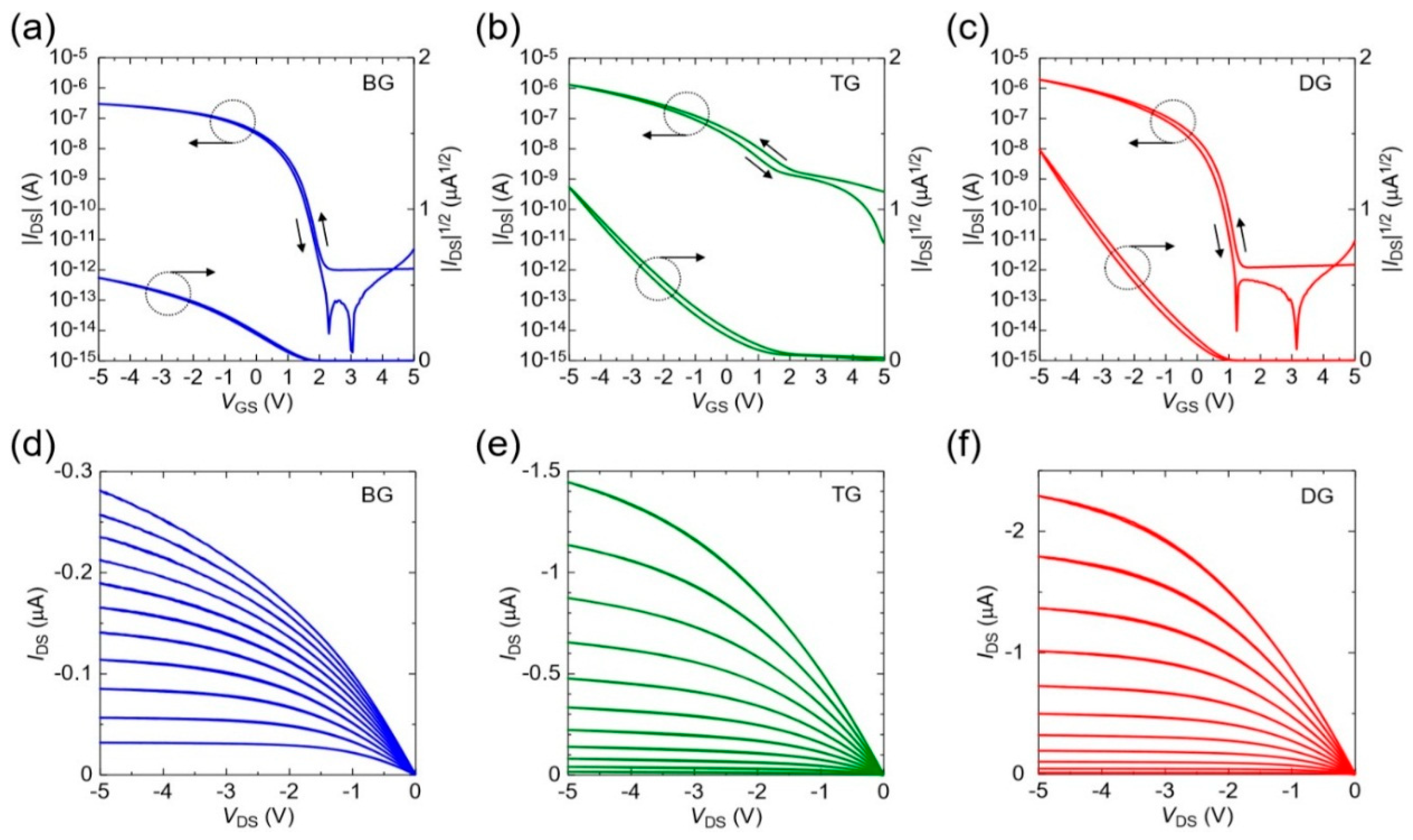
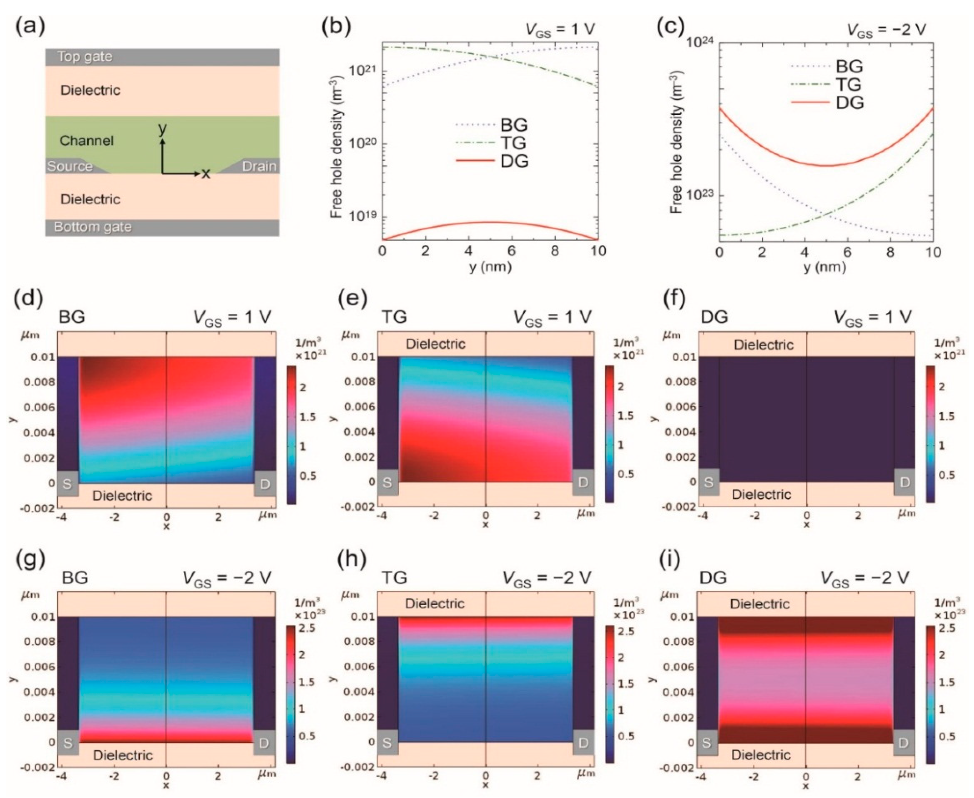
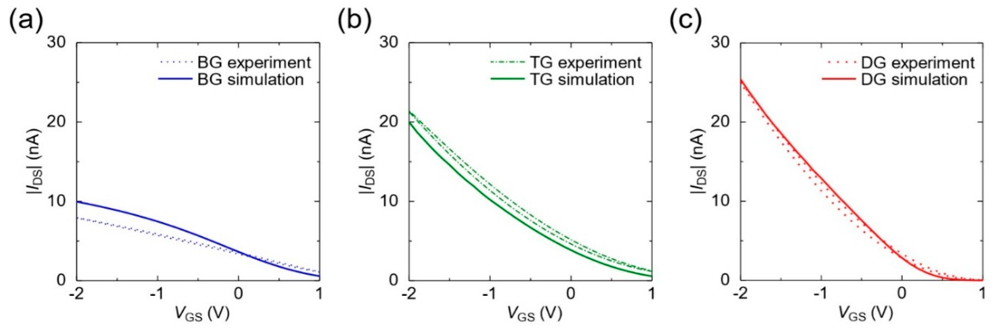
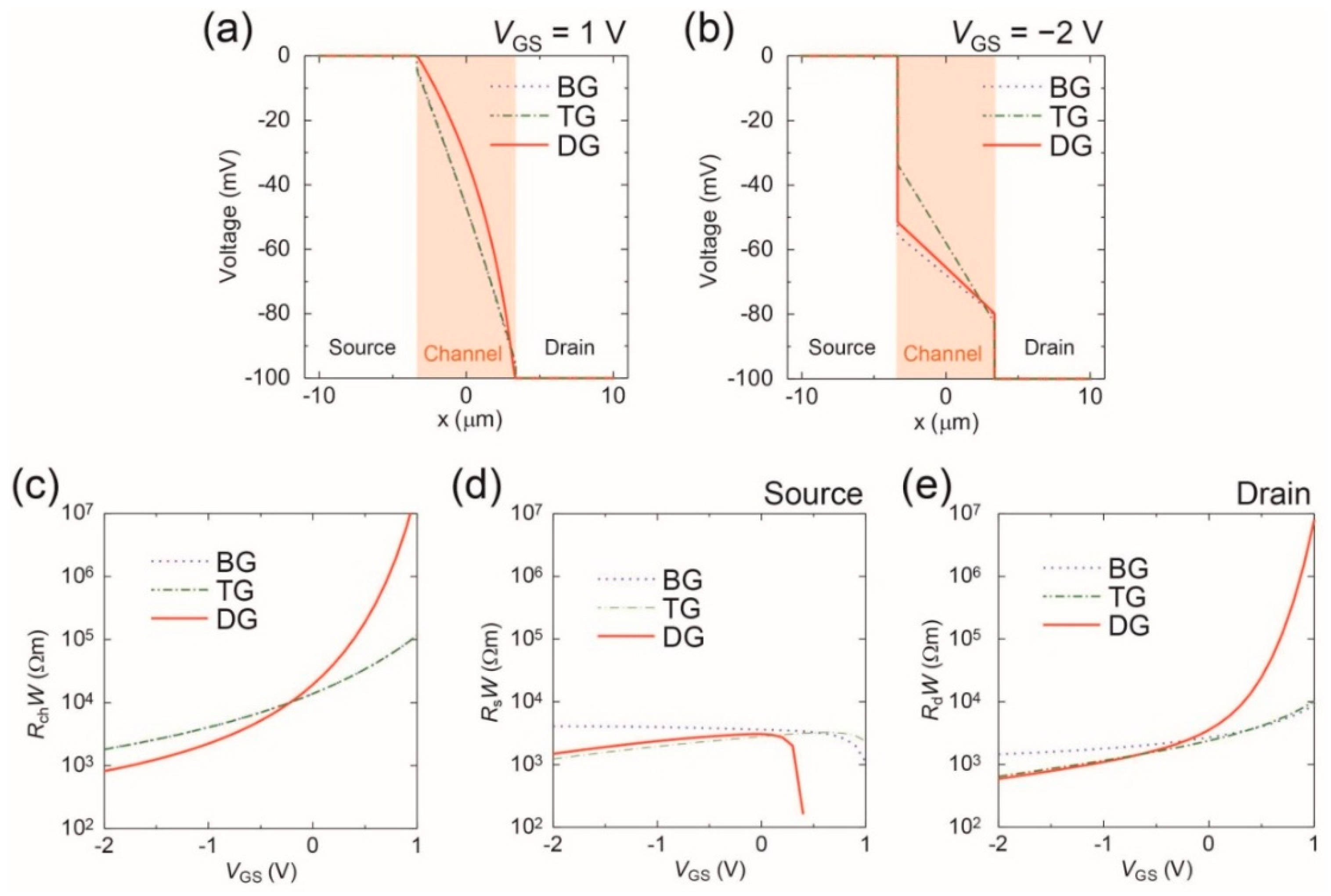
3. Results and Discussion
4. Conclusions
Author Contributions
Funding
Acknowledgments
Conflicts of Interest
References
- Someya, T.; Sekitani, T.; Iba, S.; Kato, Y.; Kawaguchi, H.; Sakurai, T. A large-area, flexible pressure sensor matrix with organic field-effect transistors for artificial skin applications. Proc. Natl. Acad. Sci. USA 2004, 101, 9966–9970. [Google Scholar] [CrossRef] [PubMed] [Green Version]
- Myny, K.; Steudel, S.; Smout, S.; Vicca, P.; Furthner, F.; van der Putten, B.; Tripathi, A.K.; Gelinck, G.H.; Genoe, J.; Dehaene, W.; et al. Organic RFID transponder chip with data rate compatible with electronic product coding. Org. Electron. 2010, 11, 1176–1179. [Google Scholar] [CrossRef]
- Wang, J.Z.; Zheng, Z.H.; Sirringhaus, H. Suppression of short-channel effects in organic thin-film transistors. Appl. Phys. Lett. 2006, 89, 083513. [Google Scholar] [CrossRef]
- Halik, M.; Klauk, H.; Zschieschang, U.; Schmid, G.; Dehm, C.; Schütz, M.; Maisch, S.; Effenberger, F.; Brunnbauer, M.; Stellacci, F. Low-voltage organic transistors with an amorphous molecular gate dielectric. Nature 2004, 431, 963–966. [Google Scholar] [CrossRef] [PubMed]
- Gelinck, G.H.; van Veenendaal, E.; Coehoorn, R. Dual-gate organic thin-film transistors. Appl. Phys. Lett. 2005, 87, 073508. [Google Scholar] [CrossRef]
- Ha, T.-J.; Sonar, P.; Dodabalapur, A. High mobility top-gate and dual-gate polymer thin-film transistors based on diketopyrrolopyrrole-naphthalene copolymer. Appl. Phys. Lett. 2011, 98, 253305. [Google Scholar] [CrossRef]
- Iba, S.; Sekitani, T.; Kato, Y.; Someya, T. Control of threshold voltage of organic field-effect transistors with double-gate structure. Appl. Phys. Lett. 2005, 87, 023509. [Google Scholar] [CrossRef]
- Hizu, K.; Sekitani, T.; Someya, T.; Otsuki, J. Reduction in operation voltage of complementary organic thin-film transistor inverter circuits using double-gate structures. Appl. Phys. Lett. 2007, 90, 093504. [Google Scholar] [CrossRef]
- Marien, H.; Steyaert, M.; van Veenendaal, E.; Heremans, P. Analog techniques for reliable organic circuit design on foil applied to an 18 dB single-stage differential amplifier. Org. Electron. 2010, 11, 1357–1362. [Google Scholar] [CrossRef]
- Marien, H.; Steyaert, M.S.J.; van Veenendaal, E.; Heremans. A Fully Integrated ΔΣ ADC in Organic Thin-Film Transistor Technology on Flexible Plastic Foil. IEEE J. Solid State Circuits 2011, 46, 276–284. [Google Scholar] [CrossRef]
- Spijkman, M.-J.; Myny, K.; Smits, E.C.P.; Heremans, P.; Blom, P.W.M.; de Leeuw, D.M. Dual-gate thin-film transistors, integrated circuits and sensors. Adv. Mater. 2011, 23, 3231–3242. [Google Scholar] [CrossRef] [PubMed]
- Myny, K.; Beenhakkers, M.J.; van Aerle, N.A.J.M.; Gelinck, G.H.; Genoe, J.; Dehaene, W.; Heremans, P. Unipolar organic transistor circuits made robust by dual-gate technology. IEEE J. Solid State Circuit 2011, 46, 1223–1230. [Google Scholar] [CrossRef]
- Marien, H.; Steyaert, M.S.J.; van Veenendaal, E.; Heremans, P. Analog building blocks for organic smart sensor systems in organic thin-film transistor technology on flexible plastic foil. IEEE J. Solid State Circuit 2012, 47, 1712–1720. [Google Scholar] [CrossRef]
- Matsui, H.; Hayasaka, K.; Takeda, Y.; Shiwaku, R.; Kwon, J.; Tokito, S. Printed 5-V organic operational amplifiers for various signal processing. Sci. Rep. 2018, 8, 8980. [Google Scholar] [CrossRef] [PubMed]
- Kumar, B.; Kaushik, B.K.; Negi, Y.S.; Goswami, V. Single and dual gate OTFT based robust organic digital design. Microelectron. Reliab. 2014, 50, 100–109. [Google Scholar] [CrossRef]
- Uemura, T.; Rolin, C.; Ke, T.-H.; Fesenko, P.; Genoe, J.; Heremans, P.; Takeya, J. On the extraction of charge carrier mobility in high-mobility organic transistors. Adv. Mater. 2016, 28, 151–155. [Google Scholar] [CrossRef] [PubMed]
- Negi, S.; Baliga, A.K.; Pandey, Y.; Mittal, P.; Kumar, B. Performance analysis of dual gate organic thin film transistor through analytical modeling. In Proceedings of the 2016 International Conference on Computing, Communication and Automation, Noida, India, 29–30 April 2016. [Google Scholar] [CrossRef]
- Takshi, A.; Dimopoulos, A.; Madden, J.D. Simulation of a dual gate organic transistor compatible with printing methods. Solid State Electron. 2008, 52, 107–114. [Google Scholar] [CrossRef]
- Xu, Y.; Darmawan, P.; Liu, C.; Li, Y.; Minari, T.; Ghibaudo, G.; Tsukagoshi, K. Tunable contact resistance in double-gate organic field-effect transistors. Org. Electron. 2012, 13, 1583–1588. [Google Scholar] [CrossRef]
- Brondijk, J.J.; Spijkman, M.; Torricelli, F.; Blom, P.W.M.; de Leeuw, D.M. Charge transport in dual-gate organic field-effect transistors. Appl. Phys. Lett. 2012, 100, 023308. [Google Scholar] [CrossRef] [Green Version]
- Kwon, J.; Takeda, Y.; Fukuda, K.; Cho, K.; Tokito, S.; Jung, S. Vertically stacked complementary organic field-effect transistors and logic circuits fabricated by inkjet printing. Adv. Electron. Mater. 2016, 2, 1600046. [Google Scholar] [CrossRef]
- Lai, S.; Cosseddu, P.; Zucca, A.; Loi, A.; Bonfiglio, A. Combining inkjet printing and chemical vapor deposition for fabrication low voltage, organic field-effect transistors on flexible substrates. Thin Solid Films 2017, 631, 124–131. [Google Scholar] [CrossRef]
- Shiwaku, R.; Matsui, H.; Hayasaka, K.; Takeda, Y.; Fukuda, T.; Kumaki, D.; Tokito, S. Printed organic inverter circuits with ultralow operating voltages. Adv. Electron. Mater. 2017, 3, 1600557. [Google Scholar] [CrossRef]
- Kondo, M.; Uemura, T.; Matsumoto, T.; Araki, T.; Yoshimoto, S.; Sekitani, T. Ultraflexible and ultrathin polymeric gate insulator for 2 V organic transistor circuits. Appl. Phys. Express 2016, 9, 061602. [Google Scholar] [CrossRef]
- Doggart, J.; Wu, Y.; Liu, P.; Zhu, S. Facile inkjet-printing self-aligned electrodes for organic thin-film transistor arrays with small and uniform channel length. ACS Appl. Mater. Interface 2010, 8, 2189–2192. [Google Scholar] [CrossRef]
- Salleo, A. Charge transport in polymeric transistors. Mater. Today 2007, 10, 38–45. [Google Scholar] [CrossRef]
- Choi, H.H.; Cho, K.; Frisbie, C.D.; Sirringhaus, H.; Podzorov, V. Critical assessment of charge mobility extraction in FETs. Nat. Mater. 2018, 17, 2–7. [Google Scholar] [CrossRef] [PubMed]
- Tanase, C.; Meijer, E.J.; Blom, P.W.M.; de Leeuw, D.M. Local charge carrier mobility in disordered organic field-effect transistors. Org. Electron. 2003, 4, 33–37. [Google Scholar] [CrossRef] [Green Version]
- Richards, T.J.; Sirringhaus, H. Analysis of the contact resistance in staggered, top-gate organic field-effect transistors. J. Appl. Phys. 2007, 102, 094510. [Google Scholar] [CrossRef]
- Kim, C.-H.; Bonnassieux, Y.; Horowitz, G. Charge distribution and contact resistance model for coplanar organic field-effect transistors. IEEE Trans. Electron Devices 2013, 60, 280–287. [Google Scholar] [CrossRef] [Green Version]


| Parameter | Value | Parameter | Value |
|---|---|---|---|
| Channel width | 732 µm | Temperature | 300 K |
| Channel length | 6.73 µm | Work function of source, drain and gate electrodes | 4.6 eV |
| Channel thickness | 10 nm | Ionization energy of semiconductor | 5.0 eV |
| Dielectric constant of insulator, εi | 3.38ε0 | The effective density of states in the valence band, Dv | 1.6 × 1020 cm−3 |
| Dielectric constant of semiconductor, εs | 4ε0 | ||
| Dielectric thickness | 140 nm | Density of trap states, Dt | 3 × 1018 cm−3 |
| Mobility along the channel, μx | 0.24 cm2/Vs | Average energy of trap states, Et | 0.15 eV |
| Mobility perpendicular to the channel, μy | 0.048 cm2/Vs | Carrier density in the neutral state, n0 | 3 × 1023 cm−3 |
| Device Structure | μsat (cm2/Vs) | VTH (V) | ION (µA) | SS (V/dec) | μlin (cm2/Vs) | ION (nA) | SS (V/dec) |
|---|---|---|---|---|---|---|---|
| VDS = −5 V, VGS > −5 V | VDS = −0.1 V, VGS > −2 V | ||||||
| BG | 0.012 ± 0.002 | 1.5 ± 0.1 | 0.23 ± 0.04 | 0.5 ± 0.3 | 0.012 ± 0.002 | 6.4 ± 0.8 | 1.6 ± 0.3 |
| TG | 0.038 ± 0.005 | 0.68 ± 0.06 | 1.5 ± 0.2 | 1.4 ± 1.0 | 0.032 ± 0.003 | 19 ± 1 | 1.4 ± 0.2 |
| DG | 0.050 ± 0.013 | 0.42 ± 0.04 | 1.9 ± 0.2 | 0.3 ± 0.1 | 0.047 ± 0.011 | 24 ± 2 | 0.4 ± 0.1 |
© 2018 by the authors. Licensee MDPI, Basel, Switzerland. This article is an open access article distributed under the terms and conditions of the Creative Commons Attribution (CC BY) license (http://creativecommons.org/licenses/by/4.0/).
Share and Cite
Shiwaku, R.; Tamura, M.; Matsui, H.; Takeda, Y.; Murase, T.; Tokito, S. Charge Carrier Distribution in Low-Voltage Dual-Gate Organic Thin-Film Transistors. Appl. Sci. 2018, 8, 1341. https://doi.org/10.3390/app8081341
Shiwaku R, Tamura M, Matsui H, Takeda Y, Murase T, Tokito S. Charge Carrier Distribution in Low-Voltage Dual-Gate Organic Thin-Film Transistors. Applied Sciences. 2018; 8(8):1341. https://doi.org/10.3390/app8081341
Chicago/Turabian StyleShiwaku, Rei, Masataka Tamura, Hiroyuki Matsui, Yasunori Takeda, Tomohide Murase, and Shizuo Tokito. 2018. "Charge Carrier Distribution in Low-Voltage Dual-Gate Organic Thin-Film Transistors" Applied Sciences 8, no. 8: 1341. https://doi.org/10.3390/app8081341
APA StyleShiwaku, R., Tamura, M., Matsui, H., Takeda, Y., Murase, T., & Tokito, S. (2018). Charge Carrier Distribution in Low-Voltage Dual-Gate Organic Thin-Film Transistors. Applied Sciences, 8(8), 1341. https://doi.org/10.3390/app8081341