Article

Stop Band Continuous Profile Filter in Empty Substrate Integrated Coaxial Line

1
Instituto de Telecomunicaciones y Aplicaciones Multimedia, Universitat Politècnica de València, 46022 Valencia, Spain
2
Departamento de Ingeniería Eléctrica, Electrónica, Automática y Comunicaciones, Universidad de Castilla-La Mancha, Escuela Politécnica de Cuenca, Campus Universitario, 16071 Cuenca, Spain
*
Author to whom correspondence should be addressed.
Appl. Sci. 2018, 8(11), 2176; https://doi.org/10.3390/app8112176
Submission received: 5 October 2018 / Revised: 2 November 2018 / Accepted: 3 November 2018 / Published: 7 November 2018
(This article belongs to the Special Issue Substrate Integrated Waveguide (SIW) and Its Applications)

Abstract

:

Featured Application

A stop band continuous profile filter is implemented for the first time in the novel empty substrate integrated coaxial line technology.

Abstract

Substrate integrated waveguides reduce the losses and increase the quality factor of resonators in communication filters when compared with traditional planar technologies, while maintaining their low-cost and low-profile characteristics. Empty substrate integrated waveguides go one step further, removing the dielectric of the substrate. One of these transmission lines is the empty substrate integrated coaxial line (ESICL), which has the advantage of being a two-conductor structure. Thus, it propagates a transversal electric and magnetic (TEM) mode, which reduces the dispersion and the bandwidth limitation of other one conductor empty substrate integrated waveguides. Continuous profile filters, at the cost of being long structures, are very easy to manufacture and design (usually no optimization is needed), and they are highly insensitive to manufacturing tolerances. In this work, a simple continuous profile filter, with a stop band response, is designed for the first time using novel ESICL technology. The influence of the design parameters on the insertion losses and fractional bandwidth is discussed. A prototype has been successfully manufactured and measured. A sensitivity analysis shows the high tolerance of the proposed stop band filter to manufacturing errors.

Graphical Abstract

1. Introduction

Over recent years, a great number of substrate integrated circuits [1] have been developed. The characteristics of these circuits are midway between the characteristics of waveguide technologies and planar circuits. They have a higher quality factor and lower insertion losses than planar circuits, while also being low profile, low cost, and easily integrable in a printed circuit board. The substrate integrated waveguide (SIW) [2] and the substrate integrated coaxial line (SICL) [3] are two proposals of substrate integrated circuits that have been a great advance in this field. Several passive components developed in these technologies, including filters [4,5], ultra-wideband filters [6,7], antennas [8,9], transitions and tapers [10,11], baluns [12,13], couplers [14,15], power dividers [16], and new transmission lines [3,17,18,19,20], have been proposed. However, although their quality factor and losses are better than those of the planar circuits, these characteristics can be further improved (without losing their compactness and low-cost manufacturing) if the dielectric substrate is removed and the waves are allowed to propagate through the air.
This is the purpose of some empty substrate integrated waveguides that have been recently proposed, such as the Modified SIW (MSIW) [21], the Empty SIW (ESIW) [22], the Air-filled SIW (AFSIW) [23], the Hollow SIW (HSIW) [24], or the Dielectricless SIW (DSIW) [25]. All these new transmission lines are integrated in a substrate and they are low profile, low cost, and have higher quality factor and less losses than the SIW, thanks to the complete or partial removal of the dielectric in the path of the electromagnetic (EM) fields. However, these are one conductor structures, which means that the fundamental mode is dispersive, with a cutoff frequency greater than zero, which limits the usable bandwidth of microwave devices implemented with such novel technologies.
These limitations can be overcome with the use of an empty substrate integrated coaxial line (ESICL). The structure of an ESICL was first used in Reference [26] for feeding an antenna, and definitively integrated in a planar circuit in Reference [27], where a transition to a classical planar line (a grounded coplanar waveguide) was proposed for the first time. The ESICL is a two-conductor transmission line, whose cross section is a rectangular coaxial built with the superposition of five layers of printed circuit board, as shown in Figure 1. This novel transmission line has been recently proposed, and until now, it has only been applied to the implementation of wide band [27] and narrow band [28] microwave filters with a non-dispersive transversal electric and magnetic (TEM) propagating mode. There are, consequently, many possible applications that remain to be explored for this novel transmission line.
One of the possible applications is its implementation in continuous profile filters. Conversely to conventional microwave filter topologies, where the filtering structure is based on sharp changes in the cross section that produce sharp impedance steps, continuous profile filters use a progressive and smooth variation of the cross section. This continuous variation has the advantage, at the cost of increasing the length of the filter, of providing a structure with much more resilience to manufacturing tolerances. Besides, the continuous profile filters can be easily and accurately designed with well-known techniques such as the ones described in Reference [29,30]. All these techniques require the phase constant to be kept constant (for the same frequency) along the propagation direction. This can be achieved with a structure that propagates a TEM mode (as is the case of the ESICL), or with a structure that propagates a non-TEM mode and that varies the cross section along the propagation direction in such a way that the cutoff frequency of this mode does not change. This can be achieved, for instance, by varying the height of a rectangular waveguide. If we vary the width of the rectangular waveguide, the cutoff frequency changes, and so it is not suitable for the traditional synthesis techniques developed for continuous profile filters. Most one-conductor substrate integrated transmission lines (SIW, ESIW, AFSIW, etc.) are H-plane structures, where the width of the rectangular cavity can be changed, but the height is fixed throughout the structure (the height of the substrate). Some efforts have been made to apply the traditional synthesis technique for continuous profile filters in H-plane structures (SIW filter) in Reference [31,32]. Although good results have been obtained, the synthesis does not provide as accurate results as when the phase constant does not change along the propagation direction. For that reason, an ESICL, with a TEM propagating mode, is an excellent candidate to implement continuous profile filters in substrate integrated waveguide technology (with lower losses than both in planar and classical SIW technologies). Although the ESICL technology is already known, and continuous profile filters have already been studied, no implementation of an ESICL filter with continuous profile has been reported to date, and so the suitability of ESICL for continuous profile filters remains unknown.
In this work, a simple continuous profile filter is implemented in an ESICL for the first time. The variation of the filter response with the design parameters is studied. A prototype is successfully manufactured and measured, and a sensitivity analysis is performed in order to test the resilience to manufacturing tolerances of this type of filter in this novel transmission line.

2. Materials and Methods

2.1. ESICL

The ESICL topology can be seen in Figure 1. Figure 1a shows the five substrate layers needed to manufacture the ESICL. These layers are the top and bottom metallic covers (layers 1 and 5), the central layer with the inner conductor of the ESICL (layer 3), and two more layers that separate the central layer from the top and bottom covers (layers 2 and 4). Layer 3 also hosts the transition from ESICL to the input and output planar accessing lines (coplanar or microstrip).
The cross section of the ESICL, after the five layers are assembled and pasted together with tin soldering paste, is depicted in Figure 1b. As can be observed, after assembling, the cross section is the same as that of a rectangular coaxial line, without any dielectric between the inner and the outer conductors. The dimensions of the cross section are included in the layout. These dimensions are the width (w) and height (t) of the inner conductor, and the width (A) and height (B) of the outer conductor.

2.2. Coupling Coefficient and Impedance

As was already demonstrated in Reference [32], a sinusoidal modulation in the profile of a transmission line produces a stop band filter response. Using the coupled-mode theory, as proposed in Reference [33], a full analytical synthesis can be achieved. To do so, the desired frequency response is used in order to determine the variation of the coupling coefficient K ( z ) along the propagation direction (z) that provides that response. For complex responses, the coupling coefficient K ( z ) can be obtained using the zeros and poles of a ideal frequency response expressed as a rational function of polynomials, as proposed in Reference [29]. However, for a simple response as in a stop band filter, the coupling coefficient can be directly expressed as a sinusoidal variation of the form [31]:
K ( z ) = A k sin 2 π Λ z + θ , z [ 0 , n p · Λ ]
where A k represents the oscillation amplitude, Λ is its period, z is the propagation direction, and θ is the phase of the sinusoidal. θ should be set to 0 in order to facilitate the subsequent manufacturing process, avoiding sharp changes in the profile at the beginning of the filter.
The value of Λ controls the central frequency of the stop band. If we want to locate the center of the stop band at a certain frequency f 0 , the period Λ should be:
Λ = π β 0
where β 0 is the phase constant of the propagating mode at the central frequency f 0 .
The amplitude A k and the length (or number of periods n p ) of the sinusoidal variation of K ( z ) control the depth of the rejection (insertion losses I L at f 0 ) and the fractional bandwidth of the stop band ( F B W ), as is described in Section 2.4.
Figure 2 shows the variation of the coupling coefficient K ( z ) for Λ = 13.52 mm, A k = 50 , n p = 15 and θ = 0 . The value of Λ has been calculated using β 0 = 232.3 rad/m, which is the phase constant of an ESICL with Z 0 = 50 Ω ( A = 6 mm, B = 2.618 mm, t = 0.866 mm and w = 1.8148 mm) at f 0 = 11 GHz.
For a device propagating a TEM mode, the relationship between the coupling coefficient and the impedance along the propagation direction is [33]:
K = 1 2 1 Z 0 d Z 0 d z
This equation can be used to express the impedance Z 0 as a function of the coupling coefficient as:
Z 0 ( z ) = Z 0 ( 0 ) e 2 0 z K ( r ) d r
Substituting the coupling coefficient of Figure 2 into Equation (4), gives the impedance variation of Figure 3. The next step is to obtain an ESICL with a profile that provides this impedance variation.

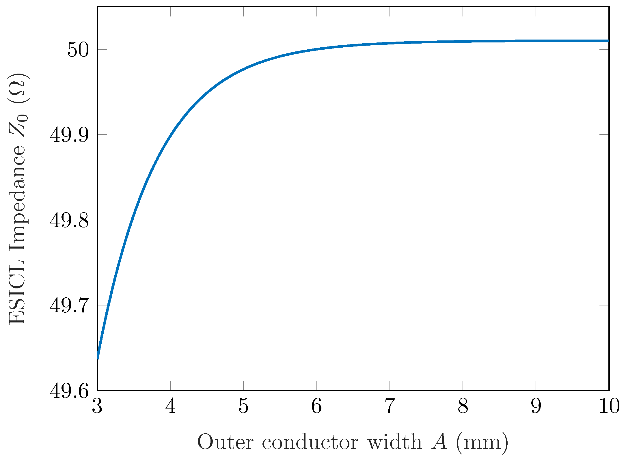
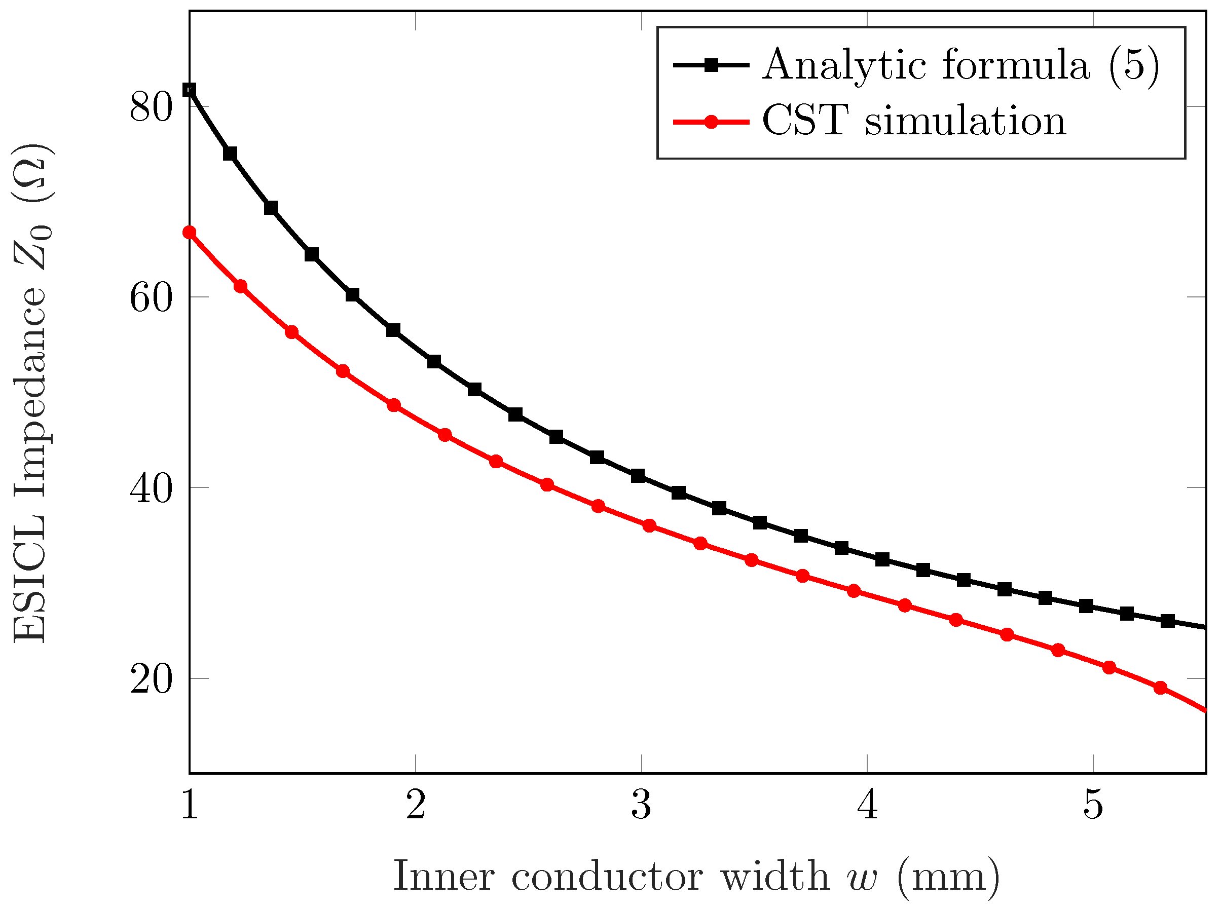
2.3. Impedance in ESICL

The impedance Z 0 of an ESICL depends on the dimensions of the cross section (A, B, t and w). The following approximation for the impedance can be found in Reference [34]:
Z 0 = η 0 4 ϵ r 1 w / B B / t 1 + 2 π ln 1 1 t / B + coth π A 2 B ( Ω )
In the ESICL, the heights of the inner and outer conductor are fixed by the height of the substrate layers. In this work, all substrate layers will be Rogers 4003C substrates of height h = 0.813 mm plus electrodeposited copper foils of 17 μ m. After taking into account the thickness of the soldering paste t = 0.866 mm and B = 2.618 mm. From Equation (5), it can be derived that Z 0 does not change significantly with the width of the outer conductor A. Figure 4 shows the variation of Z 0 with A using Equation (5), and fixing the other dimensions of the cross section. It can be observed that for A 6 mm, the impedance is almost constant. So A is fixed to 6 mm, and once A, B and t are fixed, Z 0 depends only on the width of the inner conductor w.
Figure 5 shows the variation of Z 0 with w, while A, B and t are fixed. This impedance was calculated with the analytic formula of Equation (5), and also with a commercial electromagnetic solver (computer simulation technology (CST) Studio). Both results are not in good agreement, so the most accurate results of the full-wave commercial simulator were considered.
It must be noted that in order to implement the stop band filter we need an impedance variation along the propagation direction as shown in Figure 3. That is, we must be able to change the impedance in a range from approximately 32 to 50 Ω . As shown in Figure 5, by changing w from 1 to 5.5 mm we can change Z 0 in a range that goes from 17 to 66 Ω , which is enough for implementing the stop band filter.
Using the relationship between Z 0 and w obtained with CST and shown in Figure 5, we can now derive the variation of the inner conductor width w ( z ) needed to achieve the variation of the impedance Z 0 ( z ) of Figure 3 that provides the desired coupling coefficient K ( z ) , and therefore, the desired stop band response. Figure 6 shows this variation w ( z ) for three different cases. In the first place, the value of w ( z ) derived using the analytic formula, which has proven to be inaccurate, is plotted with a solid red line. Next, the accurate value of w ( z ) computed with the impedance obtained with CST is plotted in solid black line. And finally, a sinusoidal approximation to the accurate value of w ( z ) is plotted in green round marks. This approximation is calculated using the following expression:
w = A w cos 2 π z Z p + P + B w
After 450 iterations, an optimization process with the Nelder Mead simplex algorithm [35] determined the optimum values of the parameters A w , B w and P for an optimum match of this sinusoidal approximation with the accurate value of w ( z ) . It gave A w = 0.8305 , B w = 2.61103 and P = 3.0817 . This approximation, which matches almost perfectly with the accurate value, was preferred to the accurate one, because it eases the modeling and simulation of the ESICL continuous profile filter in the electromagnetic simulator.

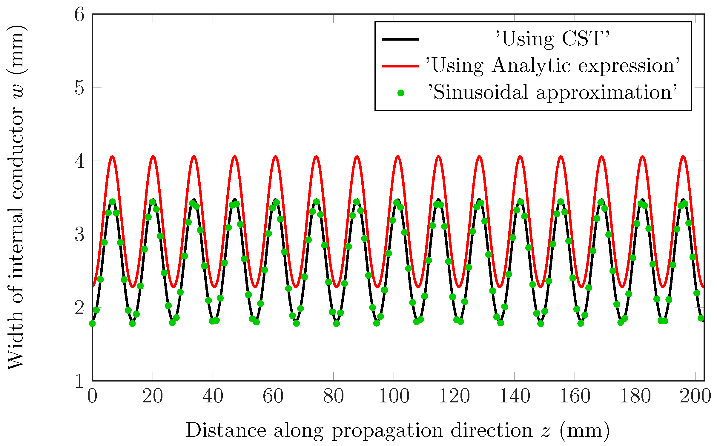
2.4. Design Procedure
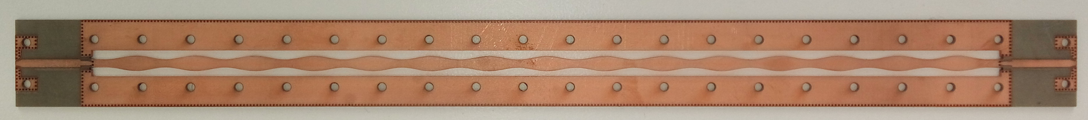
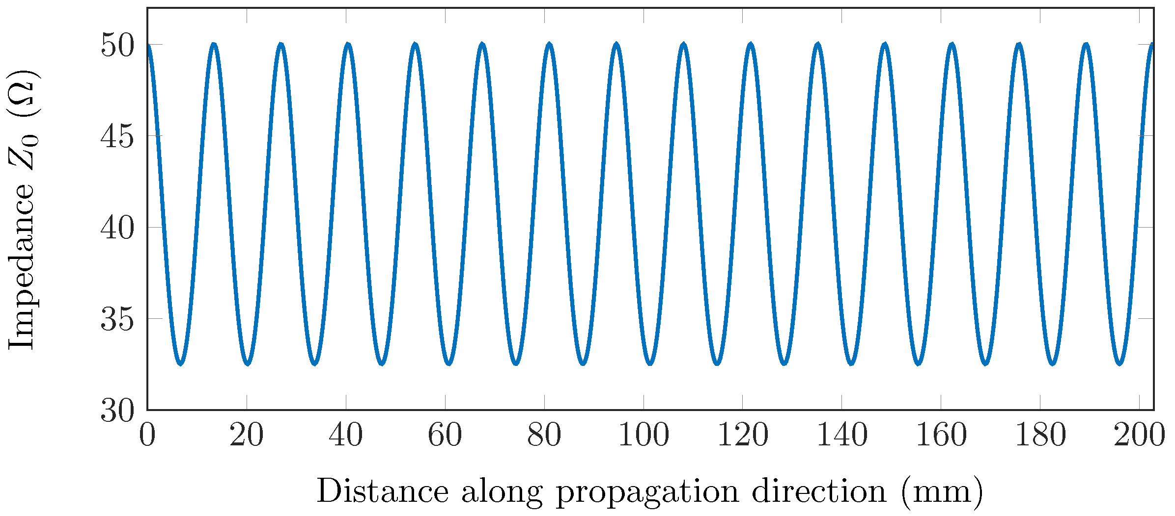
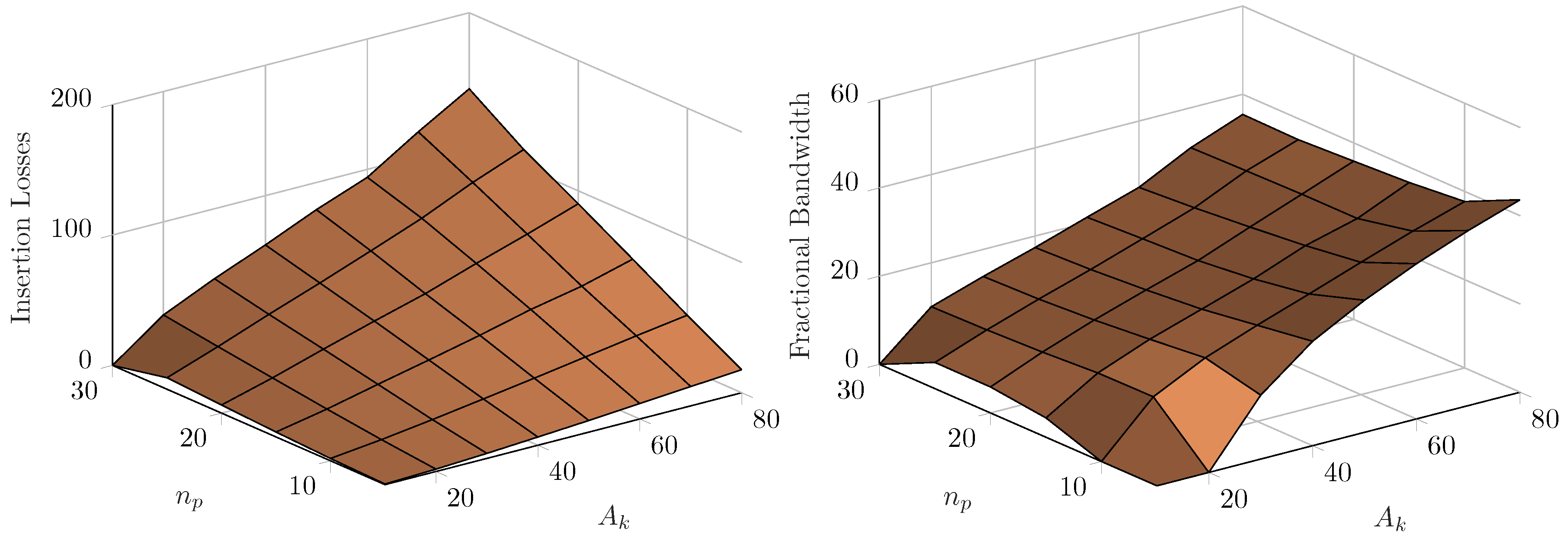
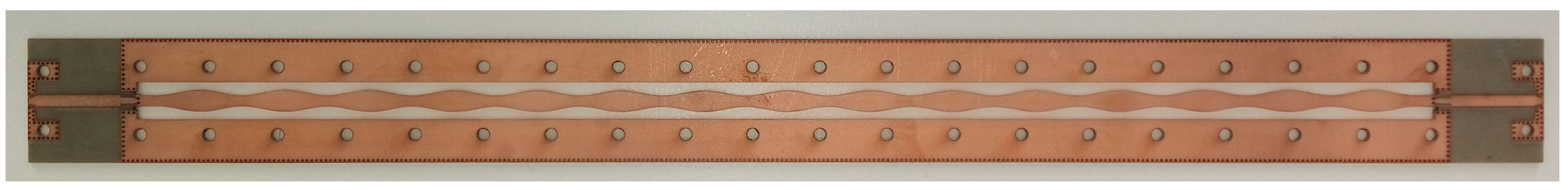
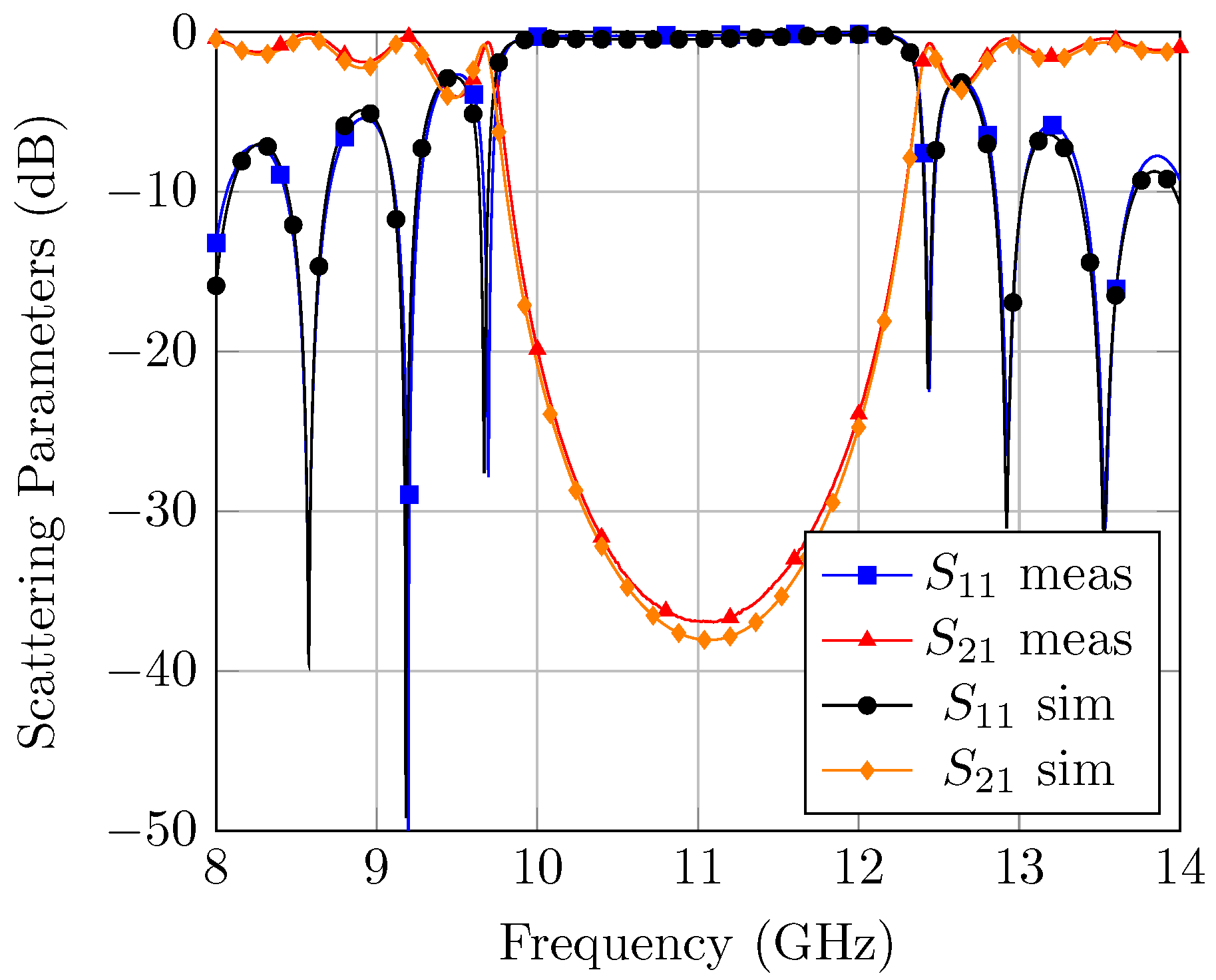
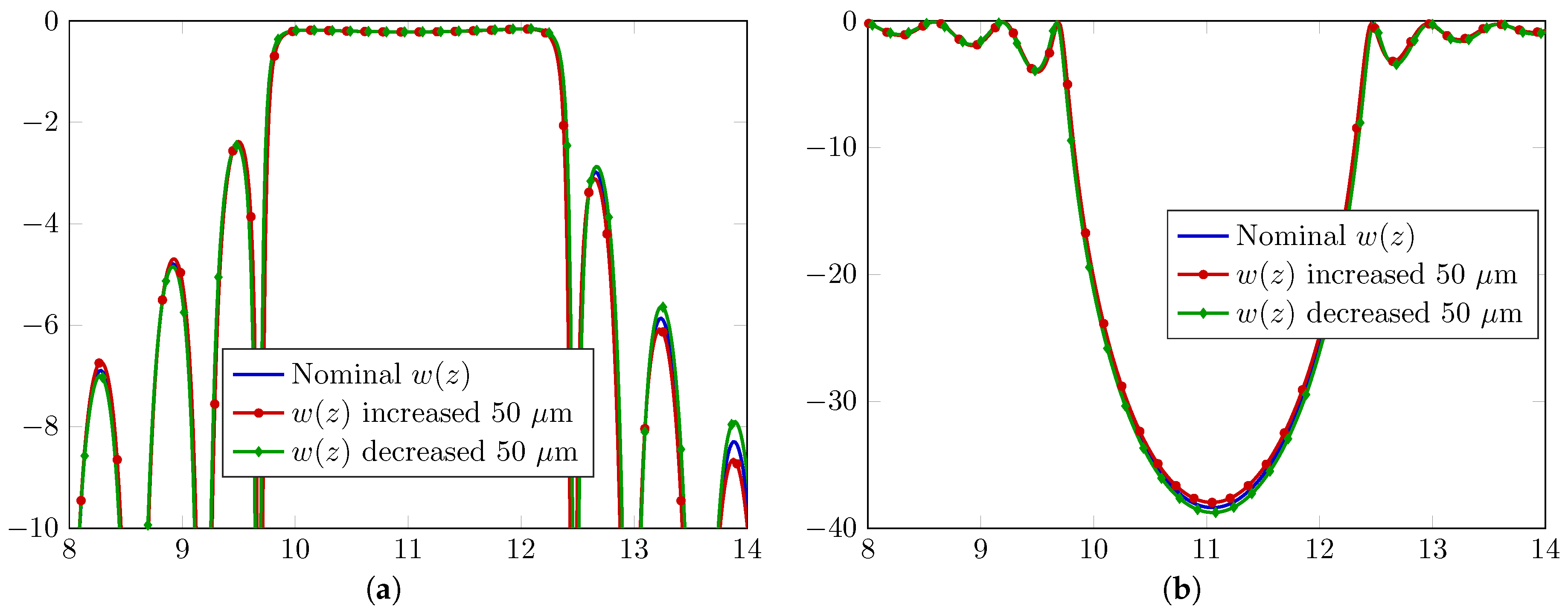
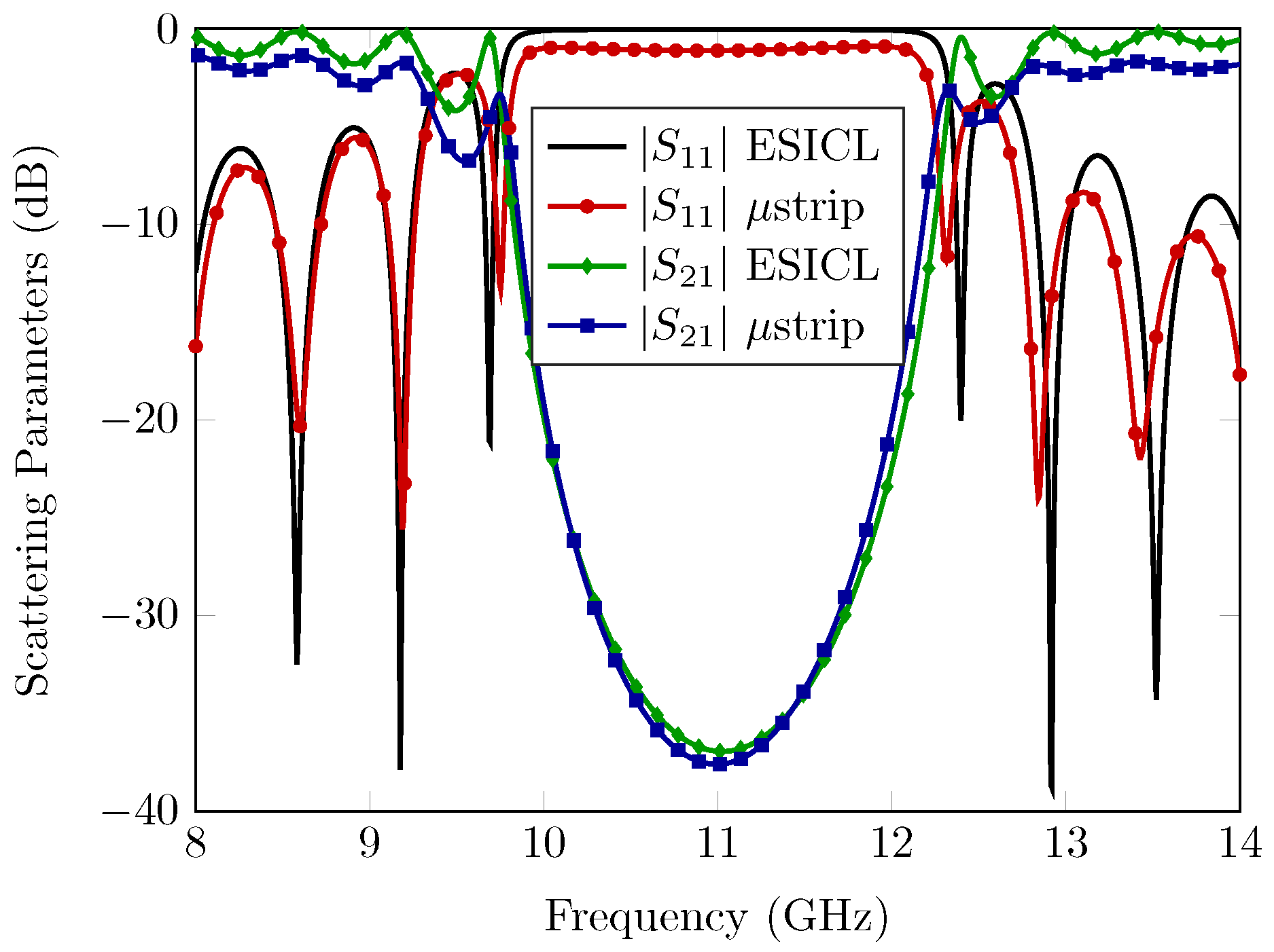
The stop band response is characterized by the central frequency ( f 0 ), the fractional bandwidth ( F B W ), and the insertion losses ( I L ) at the central frequency. These characteristics are determined by the amplitude ( A k ), period ( Λ ), and length (number of periods n p ) of the sinusoidal variation of the coupling coefficient along the propagation direction (see Equation (1)).
As already discussed in previous sections, the central frequency can be directly adjusted with the period Λ using Equation (2).
The challenge is to determine the adequate value of A k and n p in order to succeed with the specifications of I L and F B W .
In order to have an insight into the influence of A k and n p in the values of I L and F B W , several simulations were performed in CST for the ESICL filter for a discrete number of values of A k and n p with A k ranging from 10 to 80, and n p ranging from 5 to 30. Additionally, the I L and F B W was computed in all possible combinations of A k and n p . In all cases, Λ was selected to provide a stop band response centered at 11 GHz. The results are depicted in Figure 7.
As it can be observed, when A k increased, the I L and the F B W both increased. In addition, when n p increased, the I L increased, and the F B W did not change significantly. This information can be useful when either performing a manual design, or properly deciding the initial point for a computer aided optimization process that optimizes the values of A k and n p until the specifications are met.

3. Results

A prototype of the ESICL continuous profile filter was manufactured and measured. The filter was designed to have the stop band centered at 11 GHz. This led to Λ = 13.52 mm. For the sinusoidal variation of the coupling coefficient, the values A k = 50 , n p = 15 and θ = 0 were used, which are the values used in Section 2. Therefore, the coupling coefficient is the one depicted in Figure 2, the variation of the impedance is the one shown in Figure 3, and the width of the inner conductor is the one plotted in Figure 6. The other dimensions of the ESICL cross section are B = 2.618 mm, A = 6 mm, t = 0.866 mm. With all these values, the simulated insertion losses at the central frequency are 37.8 dB, and the fractional bandwidth is 23.8%.
The prototype was manufactured with Rogers 4003C substrates of height h = 0.813 mm, with electrodeposited copper foils of 17 μ m, and substrate permittivity ε r = 3.55 .
The manufactured prototype is shown in Figure 8. The manufacture of the ESICL filter follows standard processes of planar circuit manufacturing (drilling, milling, and electrodeposition). First, the ESICL via holes were drilled and the lateral walls were cut. Then, the substrate was metallized using electroplating. This metallized the via holes and the lateral walls. Next the accessing planar lines and the transitions were milled. Finally, all the layers were piled together using alignment screws, and soldered using tin soldering paste. An LPKF Protolaser U3 circuit board plotter was used for the drilling, cutting, and milling. An LPKF Mini Contac RS through-hole electroplating system was used for electroplating, and an LPKF ProtoFlow S reflow oven was used for curing the tin soldering paste.
Figure 9 compares the simulated and measured scattering parameters of the ESICL prototype. As can be observed, there is a very good agreement between the simulation and measurements.
One of the advantages of continuous profile filters is supposed to be the high tolerance to manufacturing errors. In order to verify this low sensitivity to variations in the dimensions of the filter, the scattering parameters of the ESICL prototype were simulated altering the width on the inner conductor ( w ( z ) ). This dimension is the most critical dimension of the filter, since this is the dimension that has a greater influence on the impedance of the ESICL. Taking into account the manufacturing tolerance of the machine used for drilling and cutting ( 50 μ m), the scattering parameters were simulated with the nominal value of w ( z ) , with w ( z ) increased by 50 μ m, and with w ( z ) decreased by 50 μ m. The results are shown in Figure 10. As can be observed, the response of the filter did not change significantly after either increasing or decreasing w ( z ) , which is consistent with the alleged advantage of this type of filters.
Finally, the performance of the continuous profile filter of Figure 8 in the ESICL was compared with the same filter implemented in microstrip technology. Figure 11 shows the simulated results for this filter in both technologies. Lossy copper (conductivity σ = 5.8 · 10 7 S/m) and lossy dielectric ( ε r = 3.55 , tan δ = 0.0027 ) were considered in the simulations. The simulations were obtained using CST. These simulations estimated a quality factor of the ESICL filter of 1547, whereas for the microstrip filter, the estimated quality factor was 348. The reflection coefficient S 11 at the central frequency (11 GHz) was –0.04 dB for the ESICL filter, and –0.91 dB for the microstrip filter. The total length of the filter was 20.3 cm in the ESICL, and 12.2 cm in the microstrip.

4. Discussion

In this work, a stop band continuous profile filter was implemented for the first time in an ESICL. The use of an ESICL has the advantages of being of low cost and of low profile, manufactured with standard planar circuits machinery. It has lower insertion losses and higher quality factors than planar circuits, and than substrate integrated waveguides filled with dielectric. Besides, since the ESICL has two conductors, it propagates a fundamental TEM mode and has lower dispersion and a higher usable bandwidth, being therefore suitable for implementing highly accurate design procedures for continuous profile filters. In this work, a very simple continuous profile filter was designed and manufactured. The influence of the design parameters on the frequency response was studied. The measurements are in good agreement with simulations. A sensitivity analysis was performed, proving that the structure has very high resilience to manufacturing errors. The results are promising for the extension of the ESICL to the implementation of other low-cost and high-quality communication devices.

5. Conclusions

A stop band continuous profile filter has been implemented for the first time in an ESICL. A sensitive analysis proves the resilience to manufacturing errors. A filter has been manufactured and successfully compared with simulations. Performance of the filter has been compared with the same filter in microstrip.

Author Contributions

Conceptualization, H.E., A.B. and A.L.B.; Methodology, D.G. and H.E.; Software, D.G.; Formal analysis, D.G. and H.E.; Validation, A.B. and A.L.B.; Investigation, D.G., H.E., A.B. and A.L.B.; Resources, A.B., H.E. and V.E.B.; Writing—Original Draft Preparation, D.G.; Writing—Review & Editing, H.E.; Visualization, D.G.; Supervision, H.E.; Project Administration, A.B. and V.E.B.; Funding Acquisition, A.B. and V.E.B.

Funding

This research was funded by Ministerio de Economía, Industria y Competitividad, Spanish Government, under Research Projects TEC2016-75934-C4-3-R and TEC2016-75934-C4-1-R.

Conflicts of Interest

The authors declare no conflict of interest. The founding sponsors had no role in the design of the study; in the collection, analyses, or interpretation of data; in the writing of the manuscript, and in the decision to publish the results.

Abbreviations

The following abbreviations are used in this manuscript:
SIWSubstrate integrated waveguide
ESIWEmpty substrate integrated waveguide
MSIWModified substrate integrated waveguide
AFSIWAir filled substrate integrated waveguide
HSIWHollow substrate integrated waveguide
DSIWDielectricless substrate integrated waveguide
ESICLEmpty substrate integrated coaxial line
SICLSubstrate integrated coaxial cine
GCPWGrounded coplanar waveguide
TEMTransversal electric and magnetic
CSTComputer Simulation Technology
ILInsertion losses
FBWFractional bandwidth

References

  1. Deslandes, D.; Wu, K. Integrated microstrip and rectangular waveguide in planar form. IEEE Microw. Wirel. Compon. Lett. 2001, 11, 68–70. [Google Scholar] [CrossRef]
  2. Deslandes, D.; Wu, K. Accurate modeling, wave mechanisms, and design considerations of a substrate integrated waveguide. IEEE Trans. Microw. Theory Tech. 2006, 54, 2516–2526. [Google Scholar] [CrossRef]
  3. Gatti, F.; Bozzi, M.; Perregrini, L.; Wu, K.; Bosisio, R.G. A Novel Substrate Integrated Coaxial Line (SICL) for Wide-Band Applications. In Proceedings of the 2006 European Microwave Conference, Manchester, UK, 10–15 September 2006; pp. 1614–1617. [Google Scholar]
  4. Zhang, D.D.; Zhou, L.; Wu, L.S.; Qiu, L.F.; Yin, W.Y.; Mao, J.F. Novel Bandpass Filters by Using Cavity-Loaded Dielectric Resonators in a Substrate Integrated Waveguide. IEEE Trans. Microw. Theory Tech. 2014, 62, 1173–1182. [Google Scholar] [CrossRef]
  5. Chu, P.; Hong, W.; Dai, L.; Tang, H.; Chen, J.; Hao, Z.; Zhu, X.; Wu, K. A Planar Bandpass Filter Implemented With a Hybrid Structure of Substrate Integrated Waveguide and Coplanar Waveguide. IEEE Trans. Microw. Theory Tech. 2014, 62, 266–274. [Google Scholar] [CrossRef]
  6. Honari, M.M.; Mirzavand, R.; Saghlatoon, H.; Mousavi, P. Two-Layered Substrate Integrated Waveguide Filter for UWB Applications. IEEE Microw. Wirel. Compon. Lett. 2017, 27, 633–635. [Google Scholar] [CrossRef]
  7. Huang, L.; Zhang, S. Ultra-Wideband Ridged Half-Mode Folded Substrate-Integrated Waveguide Filters. IEEE Microw. Wirel. Compon. Lett. 2018, 28, 579–581. [Google Scholar] [CrossRef]
  8. Yang, T.Y.; Hong, W.; Zhang, Y. Wideband Millimeter-Wave Substrate Integrated Waveguide Cavity-Backed Rectangular Patch Antenna. IEEE Antennas Wirel. Propag. Lett. 2014, 13, 205–208. [Google Scholar] [CrossRef]
  9. Liu, J.; Jackson, D.R.; Long, Y. Substrate Integrated Waveguide (SIW) Leaky-Wave Antenna With Transverse Slots. IEEE Trans. Antennas Propag. 2012, 60, 20–29. [Google Scholar] [CrossRef]
  10. Caballero, E.D.; Martinez, A.B.; Gonzalez, H.E.; Belda, O.M.; Esbert, V.B. A novel transition from microstrip to a substrate integrated waveguide with higher characteristic impedance. In Proceedings of the 2013 IEEE MTT-S International Microwave Symposium Digest (MTT), Seattle, WA, USA, 2–7 June 2013; pp. 1–4. [Google Scholar]
  11. Deslandes, D. Design equations for tapered microstrip-to-Substrate Integrated Waveguide transitions. In Proceedings of the 2010 IEEE MTT-S International Microwave Symposium, Anaheim, CA, USA, 23–28 May 2010; pp. 704–707. [Google Scholar]
  12. Zhang, Z.Y.; Wu, K. A Broadband Substrate Integrated Waveguide (SIW) Planar Balun. IEEE Microw. Wirel. Compon. Lett. 2007, 17, 843–845. [Google Scholar] [CrossRef]
  13. Zhu, F.; Hong, W.; Chen, J.X.; Wu, K. Ultra-Wideband Single and Dual Baluns Based on Substrate Integrated Coaxial Line Technology. IEEE Trans. Microw. Theory Tech. 2012, 60, 3062–3070. [Google Scholar] [CrossRef]
  14. Ali, A.; Aubert, H.; Fonseca, N.; Coccetti, F. Wideband two-layer SIW coupler: design and experiment. Electron. Lett. 2009, 45, 687–689. [Google Scholar] [CrossRef]
  15. Patrovsky, A.; Daigle, M.; Wu, K. Coupling mechanism in hybrid SIW–CPW forward couplers for millimeter-wave substrate integrated circuits. IEEE Trans. Microw. Theory Tech. 2008, 56, 2594–2601. [Google Scholar] [CrossRef]
  16. Gatti, F.; Bozzi, M.; Perregrini, L.; Wu, K.; Bosisio, R.G. A new wide-band six-port junction based on substrate integrated coaxial line (SICL) technology. In Proceedings of the MELECON 2006—2006 IEEE Mediterranean Electrotechnical Conference, Malaga, Spain, 16–19 May 2006; pp. 367–370. [Google Scholar]
  17. Xu, F.; Wu, K. Substrate Integrated Nonradiative Dielectric Waveguide Structures Directly Fabricated on Printed Circuit Boards and Metallized Dielectric Layers. IEEE Trans. Microw. Theory Tech. 2011, 59, 3076–3086. [Google Scholar] [CrossRef]
  18. Hong, W.; Liu, B.; Wang, Y.; Lai, Q.; Tang, H.; Yin, X.X.; Dong, Y.D.; Zhang, Y.; Wu, K. Half Mode Substrate Integrated Waveguide: A New Guided Wave Structure for Microwave and Millimeter Wave Application. Proceedigns of the 2006 Joint 31st International Conference on Infrared Millimeter Waves and 14th International Conference on Teraherz Electronics, Shanghai, China, 18–22 September 2006; p. 219. [Google Scholar]
  19. Cassivi, Y.; Wu, K. Substrate integrated nonradiative dielectric waveguide. IEEE Microw. Wirel. Compon. Lett. 2004, 14, 89–91. [Google Scholar] [CrossRef]
  20. Deslandes, D.; Bozzi, M.; Arcioni, P.; Wu, K. Substrate integrated slab waveguide (SISW) for wideband microwave applications. In Proceedings of the IEEE MTT-S International Microwave Symposium Digest, Philadelphia, PA, USA, 8–13 June 2003; Volume 2, pp. 1103–1106. [Google Scholar]
  21. Ranjkesh, N.; Shahabadi, M. Reduction of dielectric losses in substrate integrated waveguide. Electron. Lett. 2006, 42, 1230–1231. [Google Scholar] [CrossRef]
  22. Belenguer, A.; Esteban, H.; Boria, V. Novel Empty Substrate Integrated Waveguide for High-Performance Microwave Integrated Circuits. Microw. Theory Tech. IEEE Trans. 2014, 62, 832–839. [Google Scholar] [CrossRef] [Green Version]
  23. Parment, F.; Ghiotto, A.; Vuong, T.P.; Duchamp, J.M.; Wu, K. Broadband transition from dielectric-filled to air-filled Substrate Integrated Waveguide for low loss and high power handling millimeter-wave Substrate Integrated Circuits. In Proceedings of the 2014 IEEE MTT-S International Microwave Symposium (IMS2014), Tampa, FL, USA, 1–6 June 2014; pp. 1–3. [Google Scholar]
  24. Jin, L.; Lee, R.M.A.; Robertson, I. Analysis and Design of a Novel Low-Loss Hollow Substrate Integrated Waveguide. IEEE Trans. Microw. Theory Tech. 2014, 62, 1616–1624. [Google Scholar] [CrossRef]
  25. Bigelli, F.; Mencarelli, D.; Farina, M.; Venanzoni, G.; Scalmati, P.; Renghini, C.; Morini, A. Design and Fabrication of a Dielectricless Substrate-Integrated Waveguide. IEEE Trans. Compon. Packag. Manuf. Technol. 2016, 6, 256–261. [Google Scholar] [CrossRef]
  26. Jastram, N.; Filipovic, D.S. PCB-Based Prototyping of 3-D Micromachined RF Subsystems. IEEE Trans. Antennas Propag. 2014, 62, 420–429. [Google Scholar] [CrossRef]
  27. Belenguer, A.; Borja, A.L.; Esteban, H.; Boria, V.E. High-Performance Coplanar Waveguide to Empty Substrate Integrated Coaxial Line Transition. IEEE Trans. Microw. Theory Tech. 2015, 63, 4027–4034. [Google Scholar] [CrossRef] [Green Version]
  28. Borja, A.L.; Belenguer, A.; Esteban, H.; Boria, V.E. Design and Performance of a High- Q Narrow Bandwidth Bandpass Filter in Empty Substrate Integrated Coaxial Line at Ku -Band. IEEE Microw. Wirel. Compon. Lett. 2017, 27, 977–979. [Google Scholar] [CrossRef]
  29. Arnedo, I.; Arregui, I.; Lujambio, A.; Chudzik, M.; Laso, M.A.G.; Lopetegi, T. Synthesis of Microwave Filters by Inverse Scattering Using a Closed-Form Expression Valid for Rational Frequency Responses. IEEE Trans. Microw. Theory Tech. 2012, 60, 1244–1257. [Google Scholar] [CrossRef]
  30. Arnedo, I.; Arregui, I.; Chudzik, M.; Teberio, F.; Lujambio, A.; Benito, D.; Lopetegi, T.; Laso, M.A.G. Direct and Exact Synthesis: Controlling the Microwaves by Means of Synthesized Passive Components with Smooth Profiles. IEEE Microw. Mag. 2015, 16, 114–128. [Google Scholar] [CrossRef]
  31. Caballero, E.D.; Roldan, I.; Urrea, V.; Chudzik, M.; Arregui, I.; Arnedo, I.; Belenguer, A. Mapping smooth profile H-plane rectangular waveguide structures to substrate integrated waveguide technology. Electron. Lett. 2014, 50, 1072–1074. [Google Scholar] [CrossRef]
  32. Schwartz, J.D.; Abhari, R.; Plant, D.V.; Azana, J. Design and Analysis of 1-D Uniform and Chirped Electromagnetic Bandgap Structures in Substrate-Integrated Waveguides. IEEE Trans. Microw. Theory Tech. 2010, 58, 1858–1866. [Google Scholar] [CrossRef]
  33. Arnedo, I.; Laso, M.A.G.; Falcone, F.; Benito, D.; Lopetegi, T. A Series Solution for the Single-Mode Synthesis Problem Based on the Coupled-Mode Theory. IEEE Trans. Microw. Theory Tech. 2008, 56, 457–466. [Google Scholar] [CrossRef]
  34. Wadell, B.C. Transmission Line Design Handbook; Artech House: Norwood, MA, USA, 1991. [Google Scholar]
  35. Nelder, J.A.; Mead, R. A simplex method for function minimization. Comput. J. 1965, 7, 308–313. [Google Scholar] [CrossRef]
Figure 1. Simplest construction of an empty substrate integrated coaxial line (ESICL) (source Reference [27]). Layer 1 and 5 are top and bottom covers; layer 3 is the central layer with transitions to planar lines; layers 2 and 4 separate the central layer from the covers. (a) 3D view of layers before assembling; (b) Cross-section of the ESICL after assembling.
Applsci 08 02176 g001
Figure 2. Variation of the coupling coefficient ( K ( z ) ) along the propagation direction ( Λ = 13.52 mm, A k = 50 , n p = 15 and θ = 0 ).
Applsci 08 02176 g002
Figure 3. Variation of the impedance ( Z 0 ) along the propagation direction.
Applsci 08 02176 g003
Figure 4. Variation of the impedance ( Z 0 ) of the ESICL as a function of the outer conductor width. B = 2.618 mm, w = 2.2823315 mm, t = 0.866 mm. The analytic formula of Equation (5) was used.
Applsci 08 02176 g004
Figure 5. Variation of the impedance ( Z 0 ) of the ESICL as a function of the inner conductor width. B = 2.618 mm, A = 6 mm, t = 0.866 mm. Comparison between analytic formula of Equation (5) and simulation with a computer simulation technology (CST) electromagnetic (EM) solver.
Applsci 08 02176 g005
Figure 6. Width of the internal conductor of the ESICL (w) that provides the desired coupling coefficient.
Applsci 08 02176 g006
Figure 7. Influence of the design parameters ( A k and n p ) on the stop band response of the ESICL filter (insertion losses and fractional bandwidth).
Applsci 08 02176 g007
Figure 8. Manufactured prototype of the ESICL continuous profile filter.
Applsci 08 02176 g008
Figure 9. Simulated and measured scattering parameters of the manufactured ESICL filter prototype.
Applsci 08 02176 g009
Figure 10. Sensitivity analysis. Comparison between scattering parameters of the filter with nominal value of the width of the inner conductor of the ESICL ( w ( z ) ), and with the width increased and decreased the manufacturing tolerance (50 μ m). (a) Reflection. (b) Transmission.
Applsci 08 02176 g010
Figure 11. Comparison of simulated results for the same continuous profile filter with ESICL and microstrip technologies.
Applsci 08 02176 g011

