Abstract
Photonic crystals are engineered structures able to control the propagation and properties of light. Due to this ability, they can be fashioned into optical components for advanced light manipulation and sensing. For these applications, a particularly interesting case study is the gyroid srs-network, a three-dimensional periodic network with both cubic symmetry and chirality. In this work we present the fabrication and characterization of three-dimensional cubically symmetric 8-srs photonic crystals derived from combination of eight individual gyroid srs-networks. We numerically and experimentally investigate optical properties of these photonic crystals and study in particular, the impact of cubic symmetry on transmission and optical activity (OA). Gyroid photonic crystals fabricated in this work can lead to the development of smaller, cheaper, and more efficient optical components with functionalities that go beyond the concept of lenses.
1. Introduction
Light can be used to collect environmental parameters and provide information about the material that it passes through. For example, polarization and orbital angular momentum of light represent fundamental optical degrees of freedom that are able to reveal physical mechanisms of light-matter interaction [1]. In order to use the information that light can collect, it is essential to develop optical devices and sensors that are able to interact with optical degrees of freedom [2]. Optical sensors are used in a wide range of research and commercial applications and play a significant role in emerging technologies [2,3,4,5]. For example, systems that implement machine learning and artificial intelligence make large use of optical sensors and require new solutions to provide new functionalities and improved performance. To harvest their full potential, optical sensors need to become smaller, cheaper, and more efficient. Moreover, they need to cover a wide range of wavelengths and incorporate new functionalities.
Photonic crystals (PhCs) are engineered structures that are able to manipulate all the degrees of freedom of light [6] and can therefore be employed as optical components for light manipulation and sensing [7,8,9,10]. For these applications, an excellent candidate is the gyroid srs-network [11,12], a three-dimensional periodic network with both cubic symmetry and chirality [13,14].
In this work we present the fabrication and characterization of three-dimensional (3D) cubically symmetric 8-srs PhCs derived from a combination of eight gyroid srs-networks. We numerically and experimentally investigate optical properties of this PhC and in particular the impact of cubic symmetry on optical activity (OA), i.e., the ability to rotate the plane of polarization of linearly polarized light. We will work in the mid-infrared (IR) spectral region, a region of tremendous scientific and technological interest [15,16]. This spectral region contains strong characteristic vibrational transitions of many important molecules, as well as two atmospheric transmission windows of 3–5 μm and 8–13 μm, which make it crucial for applications in fields such as night vision, IR astronomy, chemistry, and meteorology [17,18].
The unique morphology of gyroid geometry imparts remarkable mechanical strength [19] and a rich variety of optical and topological phenomena, from linear and circular dichroism (CD) (different in transmission for left and right circularly polarized light) to OA [20] and the recent demonstration of type-I Weyl points [2,3]. Geometrically, it is possible to intertwine more than one like- or opposite-handed gyroid srs-network into cubically symmetric structures, which enables engineering of network transmission and polarization properties. Combination of eight identical and equal handed gyroid srs-networks creates the so-called 8-srs network (Figure 1a–c), a body-centered cubic (BCC) structure belonging to the symmetry group I432 [13]. Despite the highly chiral nature of the geometry, the 8-srs network prohibits CD due to the presence of four-fold rotational symmetry [13]. Secondly, it was shown that the 8-srs network possesses a high degree of OA [13,20]. This degree of rotation was found to be comparable to that of metallic or plasmonic metamaterials [21,22], but as the network can be made using dielectric materials, OA is accompanied by low loss and high, almost unity transmission.
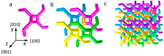
Figure 1.
Formation of an 8-srs network. (a) Typical component of a right handed 1-srs network. (b) Three copies of the 1-srs network are translated by half a unit cell along [100], [010], and [110] crystallographic directions to form a 4-srs network. (c) A single copy of the 4-srs network is translated by 1/4 of a unit cell along the [111] crystallographic direction to obtain an 8-srs network.
Experimentally, many micro- and nano-fabrication methods can be used for accurate formation of PhCs and metamaterials from single and double srs-networks [23,24,25,26,27]. For more complex composite networks such as 8-srs and for a high degree of design flexibility, the direct laser writing (DLW) technique has proven to be particularly valuable [20,28,29,30,31,32,33,34] for PhC formation. However, the DLW method suffers from an elongated cross-section of the writing focal spot, i.e., unequal sizes in lateral and vertical axes of the voxel. This leads to a breaking of cubic symmetry, which affects optical performance of fabricated structures [33]. Various methods have been developed to correct for asymmetry due to elongation of the focal spot, including apodization [35] and multi-line writing techniques [36,37]. Whilst these methods can significantly reduce elongation, to remove asymmetry completely the most effective method is galvo-dithered direct laser writing (GD-DLW) [29,30,31,33]. This fabrication method uses a galvo-mirror system to trace the focal spot in a circular motion within the focal plane. The circular motion exposes a larger lateral volume of material, whilst simultaneously reducing total exposure in the axial direction. Accordingly, asymmetry of the exposed volume can be reduced (Figure 2a).
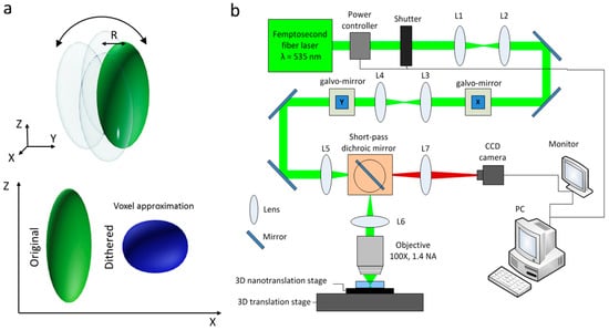
Figure 2.
Galvo-dithered direct laser writing (GD-DLW) system. (a) Illustration of circular dithered correction applied by galvo-mirrors. Radius of the dithered correction, R, is comparable to the voxel resolution. This causes the fabrication voxel to become shorter in the Z direction, improving overall resolution of the 3D fabrication method and leading to correction of voxel asymmetry. (b) Schematic of the GD-DLW setup.
In the following we will describe our method for fabricating cubically symmetric 8-srs PhCs with an operative wavelength in the mid-IR using a custom-made GD-DLW system. Finally, we present and discuss results of numerical and experimental characterization of 8-srs PhCs.
2. Materials and Methods
2.1. Galvo-Dithered Direct Laser Writing
The 8-srs PhCs were fabricated using a GD-DLW system (Figure 2b). The GD-DLW setup consists of illumination with a frequency doubled femtosecond laser (Coherent Fidelity 2) with an operating wavelength of 535 nm. Pulse width is 55 fs and repetition rate is 70 MHz. Power of the laser beam is controlled electronically using a rotating half-wave plate and linear polarizer. A mechanical shutter is used to control light exposure during fabrication. The most important addition to the GD-DLW setup is the introduction of two computer-controlled galvo-mirrors, electromechanical instruments that deflect a light beam with a mirror on receipt of an electronic signal. Using galvo-mirrors, the angle of the laser beam is modulated and steered into an oil immersion objective (100X, 1.4 N.A., Olympus, Tokyo, Japan) using a 4-f imaging system. Radius of the dithered correction, R, is comparable to the voxel resolution. This causes the fabrication voxel to become larger in lateral directions and shorter in the axial direction, improving overall resolution of the 3D fabrication method and leading to a correction of voxel asymmetry. A piezoelectric nano-translation stage (Physik Instrumente, Karlsruhe, Germany) mounted on a stepper motor controller (Thorlabs, Newton, NJ, USA) was used to trace out microstructures in a photoresist. A zirconium-based hybrid organic-inorganic photoresist was used to create templates due to its excellent resistance to shrinkage [38]. GD-DLW of 3D microstructures starts by writing the top unit cell layer to ensure the laser passes through a homogeneous material, as the fabrication system is in an inverted configuration. The bottom layer is intentionally written 3 µm below the glass-polymer interface to ensure the microstructure will be attached to the glass coverslip over the entire area of the microstructure. Failing to do this procedure may result in the microstructure being written entirely within the polymer and being lost during the wash out process. After the GD-DLW procedure, the sample is rinsed in a 1-Propanol:2-Propanol (30:70) solvent mixture for 60 min and then dried at room temperature.
2.2. Experimental Characterization
For optical characterization a commercial Fourier-transformed infrared spectrometer (Vertex 70, Bruker, Billerica, Massachusetts, USA) coupled with an infrared microscope (Hyperion 2000, Bruker, Bruker, Billerica, Massachusetts, USA) was used to measure transmission spectra of 8-srs PhCs placed between both parallel and crossed linear polarizers. For the parallel condition, both input and output polarizers were aligned to the x-axis and we denote transmission Txx. For the crossed condition, input and output polarizers were aligned to the x- and y-axis respectively and we denote transmission Txy. For each measurement, transmission spectra were normalized relative to transmission through the silica substrate and illumination angle was limited to 8° using a pinhole in the light source plane of the optical path, such that light was incident mostly (but not completely) along the [001] axis of the network.
For structural characterization, scanning electron microscopy (SEM) and focused ion beam (FIB) milling (FEI Scios Dualbeam FIBSEM, Thermo Fischer Scientific, Waltham, MA, USA) were utilized to image 8-srs PhCs along both the [001] and [011] directions. SEM images were used to determine lateral and axial line widths of the network segments respectively and FIB milling was utilized to enable observation of the interior 8-srs network morphology.
2.3. Simulations
Transmission simulations were conducted to evaluate transmission properties of 8-srs networks using the finite element method software (CST Microwave Studio). Numerical simulations assumed periodic boundary conditions laterally and four-unit cell repetitions along the propagation direction, i.e., along the [001] direction. The effect of the converging beam (α = 8°) was taken into consideration by using a moving-average filter to approximate focusing conditions numerically from a single normal-incidence numerical simulation. Geometrical parameters for calculation were taken from measured SEM images: A unit cell size of 3.5 µm, a rod diameter in the xy plane of 550 nm, and a refractive index of 1.52 [33].
3. Results and Discussion
3.1. Fabrication
In this section, we demonstrate advantages of the GD-DLW method over traditional DLW by fabricating cubically symmetric 8-srs PhCs. This fabrication method is described in the Materials and Methods (Section 2.1). A key feature of the GD-DLW method is its ability to increase exposure in lateral dimensions whilst slightly reducing exposure in axial directions, leading to a correction of voxel asymmetry (Figure 2).
The impact of GD-DLW on symmetry and resolution of PhCs can be seen in Figure 3, which shows SEM images of fabricated structures. To clearly visualize effects of GD-DLW we considered 2-srs networks (two intertwined srs-networks), a structure with a simple geometry compared to 8-srs networks. Figure 3a shows a SEM image along the [011] direction of a 2-srs network fabricated with traditional DLW. Axial and lateral linewidths of ΔZ = 1835 nm and ΔX = 581 nm produce an aspect ratio of e = 3.159 (Figure S1). In comparison, Figure 3b shows the corresponding SEM image for a 2-srs network fabricated with GD-DLW. Lateral and axial linewidths are ΔZ = 651 nm and ΔX = 649 nm respectively, corresponding to an aspect ratio of e = 1.003 and a cubically symmetric 8-srs network (Figure S1).
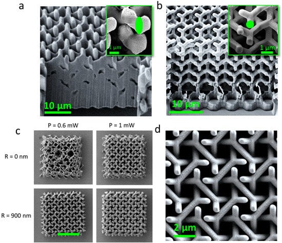
Figure 3.
Fabrication results. SEM images of focused ion beam cut polymer achiral 2-srs networks fabricated with (a) traditional direct laser writing (DLW) method and (b) GD-DLW showing a transition from elliptical to circular cross section respectively. In the inserts, cross sections are highlighted in green. (c) Top view of 8-srs PhCs fabricated using both DLW and GD-DLW. (d) Top view of an optimized 8-srs PhC.
In addition to the ability to regain cubic symmetry, use of GD-DLW also enables improvements in fabrication resolution. Figure 3c shows a qualitative comparison of 8-srs networks fabricated at various fabrication powers and dithering radius (See Figure S2 for a complete matrix). Under traditional DLW conditions (R = 0 nm) 8-srs networks fabricated with powers from 0.6 to 1.0 mW are significantly distorted, due to bending and collapse of their individual network segments. When GD-DLW is applied (R = 900 nm), 8-srs networks are mostly undistorted when fabricated with the same fabrication powers, despite the inherent reduction influence that results from dithering.
These results show that not only can cubic symmetry be achieved with GD-DLW, but that fabrication powers (and hence fabrication line-widths and resolutions) previously inaccessible (e.g., 0.6 mW) can be accessed when GD-DLW is implemented. This agrees with similar observations for simple 1-srs networks [37] and has enabled us to intricately intertwine eight cubically symmetric 1-srs networks (with lattice constants of 3.5 µm) without intersection, such as that shown in Figure 3d.
3.2. Impact of Cubic Symmetry on Optical Activity
To understand and quantify the effect of cubic symmetry on transmission properties of 8-srs PhCs, we simulated transmission spectra for structures with different aspect ratios, corresponding to the different radius, R, of the galvo-dithered (GD) correction. In a perfectly symmetric case, the focal spot of the writing laser beam is spherical and this is reflected into the model by utilizing an aspect ratio of e = 1. In other cases, the non-spherical focal spot has an elliptical shape and is implemented in the model by utilizing an aspect ratio e ≠ 1, as shown in inserts in Figure 4. If the radius of the GD correction is smaller than elongation of the focal spot (under-correction case), we have elongated features with an aspect ratio e > 1 (axial dimension being greater than lateral dimension). If the radius of the GD correction is larger than the elongation (over-correction), the aspect ratio is e < 1.
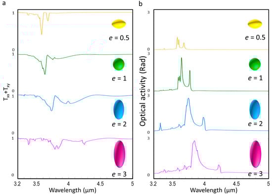
Figure 4.
Simulation of transmission and optical activity (OA). (a) 8-srs transmission as a function of aspect ratio, e. (b) 8-srs OA as a function of aspect ratio, e.
Transmission spectra were obtained by a well-established finite element method approach (see Materials and Methods section) and simulation inputs were the geometric parameters measured from SEM images; a unit cell size of 3.5 µm and rod diameter of 550 nm. Numerical simulations in Figure 4a shows that position, intensity, and width of photonic stop bands (PSB) are strongly related to the aspect ratio. In the perfectly symmetric case (e = 1) PSB is 200 nm wide and centred at 3.6 µm. When cubic symmetry is broken and e > 1, PSB undergoes a redshift, broadening, and a drop-in strength. For e = 3, PSB is redshifted by 200 nm, increases in strength by 40%, and width is increased by 50% compared to the perfectly symmetric case (e = 1). When e < 1 PBS intensity does not change, but in this case PSB undergoes a blueshift of 50 nm and PSB bandwidth decreases by approximately 50%.
Since 8-srs PhCs belong to the I432 symmetry group, they possess remarkable chiral-optical properties [13], in particular OA. To quantify OA numerically, finite element simulations were conducted to evaluate the level of linear polarization rotation. The 8-srs networks were excited with a single linearly polarized plane wave oriented along the x-axis and transmission coefficients of both unconverted (Txx) and converted (Txy) polarization components were recorded. The level of OA for networks was then calculated according to equation [13]:
The calculated OA for different values of aspect ratio are reported in Figure 4b.
In the symmetric case (e = 1) OA is centred at 3.6 µm and 200 nm wide. When cubic symmetry is broken and e < 1, we observe a drop in OA of more than 60% and a blueshift of 50 nm compared to the e = 1 case. However, when e is increased and assumes values > 1, OA intensity remains constant but undergoes a redshift and broadening. Simulation for e = 3, for example, shows a redshift of 200 nm and bandwidth of OA is more than tripled. When cubic symmetry is broken (e > or e < 1), we observe redshift or blueshift in transmission dips respectively and a drop in transmission intensity.
3.3. Experimental Characterization
To characterize optical properties of 8-srs PhCs fabricated with GD-DLW and to quantify the effect of cubic symmetry on OA and transmission, we compared simulated transmission and OA spectra (Figure 5a,b) calculated for structures with a different aspect ratio with experimental spectra of structures fabricated with different R (Figure 5c,d). Both experimental and simulated PhCs have a lattice constant of 3.5 µm and rod diameter of 550 nm in the xy plane.
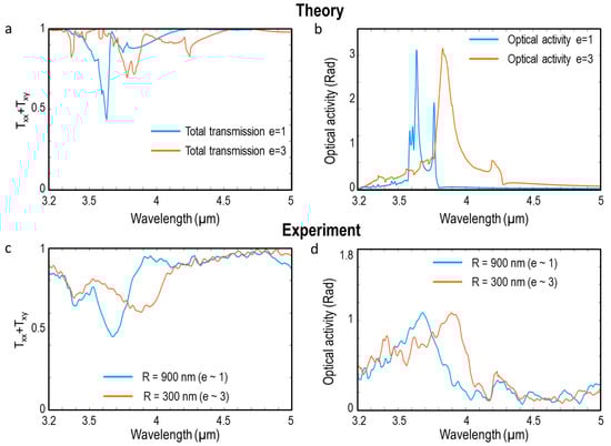
Figure 5.
Comparison of experimental and theoretical results. (a) Theoretical transmission and (b) theoretical OA calculated for 8-srs PhCs with lattice constant of 3.5 µm and rod diameter of 550 nm for aspect ratio e = 1 (blue) and e = 3 (orange). (c) Experimental transmission and (d) experimental OA for 8-srs PhC fabricated via GD-DLW with different GD radius (R): 900 nm (e~1) (blue) and 300 nm (e~3) (orange).
Optical transmissions for different light polarizations were obtained using a Fourier-transformed infrared spectrometer measured with angle resolution along the [001] direction of PhCs, as described in the Materials and Methods section.
Figure 5c,d shows total experimental transmission (Txx + Txy) and OA respectively, across 8-srs PhCs with a lattice constant of 3.5 µm, fabricated with GD radius of R = 900 nm (blue) corresponding to an aspect ratio of e ≈ 1 and R = 300 nm (orange) corresponding to an aspect ratio of e ≈ 3. For the complexity of the structure and the chosen period of 3.5 µm, the transmission spectra of PhCs fabricated with R = 0 nm, corresponding to simple DLW, do not show any PSB (Figure S3), the index of a poor quality structure. Corresponding simulated total transmission and OA for structures of the same geometry can be seen in Figure 5a,b. Whilst the 8° focused beam, presence of material absorptions, and scattering losses in experiments broaden and weaken spectral features in the experimental results, there is good agreement between experiment and simulated behavior. Specifically, changes in spectral position, transmission suppression, and stop-gap bandwidth compare well with changes expected from simulations. In the case of OA, we observe that strength of OA remains constant as expected, whilst bandwidth increases. Quantitatively, we conserve peak OA of 1 Rad at a wavelength of 4.68 µm and 4.97 µm through our 8-srs PhCs of height 14 µm (4-unit cells) and we observe a minimum OA of 0.5 Rad across a bandwidth of 500 nm and 780 nm, centered at a wavelength of 4.50 µm and 4.20 µm for e ≈ 1 and e ≈ 3, respectively.
4. Conclusions
We have fabricated 8-srs PhCs using a symmetry-preserving laser direct fabrication method. The numerically and experimentally characterized transmission properties of 8-srs networks reveal the influence of cubic symmetry on optical properties. Specifically, we have demonstrated that by using GD correction, cubic symmetry of the structures is greatly improved. Optically, OA and PSB intensity, position, and bandwidth can be modulated by adjusting cubic symmetry. The 8-srs PhCs fabricated in this work are optically active materials that can finely control in three-dimensions the propagation of light in mid-IR and tune rotation of the polarization plane of light by 1 Rad through a layer of four-unit cells. The 8-srs PhCs can be considered for gas or liquid sensing due to their ability to detect refractive index changes in the material they are immersed in. OA through a gas filled interaction volume serves as a sensing signal for determination of gas composition or concentration. Moreover, thickness, PSB, and OA are crucial prerequisites for many ultra-thin optical devices such as optical filters [39,40,41] and polarization rotators [42,43].
Supplementary Materials
The following are available online at http://www.mdpi.com/2076-3417/8/11/2104/s1, Figure S1: Axial and lateral linewidths obtained from SEM images taken along the [011] direction. (a) In this configuration the sample is tilted by an angle of 45°, therefore the lateral dimension ΔX can directly be extracted by the images. To obtain the real ΔZ value, it is necessary to multiply the measured value by √2. (b) SEM image of 2-srs PhC fabricated using DLW and corresponding values of ΔX, ΔZ and e. (c) SEM image of 2-srs PhC fabricated using GD-DLW and corresponding values of ΔX, ΔZ and e. The software used for the measurements is ImageJ; Figure S2: SEM image of 8-srs PhCs fabricated using GD-DLW demonstrating the beneficial effects of the galvo-dithering on the mechanical stability. The power of the laser (P) is varied from 0.6 mW to 1 mW and the galvo-dithering radius (R) is varied from 0 nm to 900 nm; Figure S3: Experimental transmission spectra for 8-srs PhC fabricated via DLW (R = 0).
Author Contributions
All authors conceived the original idea. E.G. carried out the PhCs fabrication, characterization and numerical calculations. All authors analyzed the results and reviewed the manuscript.
Funding
This research was conducted by the Australian Research Council Centre of Excellence for Ultrahigh-bandwidth Devices for Optical Systems (project number CE110001018).
Acknowledgments
Min Gu acknowledges support from the Australian Research Council Centre of Excellence for Ultrahigh-bandwidth Devices for Optical Systems (project number CE110001018). We thank the support of the RMIT Microscopy and Microanalysis Facility at RMIT University.
Conflicts of Interest
The authors declare no conflicts of interest. The funders had no role in design of the study; collection, analyses, or interpretation of data; writing of the manuscript; or the decision to publish results.
References
- Cvijetic, N.; Milione, G.; Ip, E.; Wang, T. Detecting lateral motion using light’s orbital angular momentum. Sci. Rep. 2015, 5, 1–7. [Google Scholar] [CrossRef] [PubMed]
- Nair, R.V.; Vijaya, R. Photonic crystal sensors: An overview. Prog. Quantum Electron. 2010, 34, 89–134. [Google Scholar] [CrossRef]
- Wang, H.; Zhang, K.Q. Photonic crystal structures with tunable structure color as colorimetric sensors. Sensors 2013, 13, 4192–4213. [Google Scholar] [CrossRef] [PubMed]
- Sabri, N.; Aljunid, S.A.; Salim, M.S.; Ahmad, R.B.; Kamaruddin, R. Toward optical sensors: Review and applications. J. Phys. Conf. Ser. 2013, 423. [Google Scholar] [CrossRef]
- González, L.A. Review on integrated optical sensors and its applications. In Proceedings of the 2017 IEEE Mexican Humanitarian Technology Conference (MHTC), Puebla, Mexico, 29–31 March 2017; pp. 170–173. [Google Scholar]
- Joannopoulos, J.D.; Johnson, S.; Winn, J.N.; Meade, R.D. Photonic Crystals: Molding the Flow of Light; Priceton University Press: Princeton, NJ, USA, 2008; ISBN 9780691124568. [Google Scholar]
- Sinibaldi, A.; Sampaoli, C.; Danz, N.; Munzert, P.; Sibilio, L.; Sonntag, F.; Occhicone, A.; Falvo, E.; Tremante, E.; Giacomini, P.; et al. Biosensors and Bioelectronics Detection of soluble ERBB2 in breast cancer cell lysates using a combined label-free/fl uorescence platform based on Bloch surface waves. Biosens. Bioelectron. 2017, 92, 125–130. [Google Scholar] [CrossRef] [PubMed]
- Sriram, R.; Baker, J.E.; Fauchet, P.M.; Miller, B.L. Two dimensional photonic crystal biosensors as a platform for label-free sensing of biomolecules. Proc. SPIE 2013, 8570. [Google Scholar] [CrossRef]
- Fischer, J.; Wegener, M. Three-dimensional optical laser lithography beyond the diffraction limit. Laser Photonics Rev. 2013, 7, 22–44. [Google Scholar] [CrossRef]
- Lim, C.Y.; Choi, E.; Park, Y.; Park, J. 3D photonic crystal-based biosensor functionalized with quantum dot-based aptamer for thrombine detection. Proc. SPIE 2014, 9127. [Google Scholar] [CrossRef]
- Schoen, A.H. Infinite Periodic Minimal Surfaces without Self-Intersections; NASA-TN-D-5541; NASA: Washington, DC, USA, 1970; p. 92.
- Dolan, J.A.; Wilts, B.D.; Vignolini, S.; Baumberg, J.J.; Steiner, U.; Wilkinson, T.D. Optical properties of gyroid structured materials: From photonic crystals to metamaterials. Adv. Opt. Mater. 2015, 3, 12–32. [Google Scholar] [CrossRef]
- Saba, M.; Turner, M.D.; Mecke, K.; Gu, M.; Schröder-Turk, G.E. Group theory of circular-polarization effects in chiral photonic crystals with four-fold rotation axes applied to the eight-fold intergrowth of gyroid nets. Phys. Rev. B Condens. Matter Mater. Phys. 2013, 88, 245116. [Google Scholar] [CrossRef]
- Saba, M.; Thiel, M.; Turner, M.D.; Hyde, S.T.; Gu, M.; Grosse-Brauckmann, K.; Neshev, D.N.; Mecke, K.; Schröder-Turk, G.E. Circular dichroism in biological photonic crystals and cubic chiral nets. Phys. Rev. Lett. 2011, 106, 103902. [Google Scholar] [CrossRef] [PubMed]
- Peng, S.; Zhang, R.; Chen, V.H.; Khabiboulline, E.T.; Braun, P.; Atwater, H.A. Three-Dimensional Single Gyroid Photonic Crystals with a Mid-Infrared Bandgap. ACS Photonics 2016, 3, 1131–1137. [Google Scholar] [CrossRef]
- Singh, V.; Lin, P.T.; Patel, N.; Lin, H.; Li, L.; Zou, Y.; Deng, F.; Ni, C.; Hu, J.; Giammarco, J.; et al. Mid-infrared materials and devices on a Si platform for optical sensing. Sci. Technol. Adv. Mater. 2014, 15, 014603. [Google Scholar] [CrossRef] [PubMed]
- Schliesser, A.; Picqué, N.; Hänsch, T.W. Mid-infrared frequency combs. Nat. Photonics 2012, 6, 440–449. [Google Scholar] [CrossRef]
- Active, H.O.W.; Policy, S.; Benefit, C.A.N.; All, U.S. Editorial Extending opportunities. Nat. Photonics 2012, 6. [Google Scholar] [CrossRef]
- Khaderi, S.N.; Deshpande, V.S.; Fleck, N.A. The stiffness and strength of the gyroid lattice. Int. J. Solids Struct. 2014, 51, 3866–3877. [Google Scholar] [CrossRef]
- Turella, F.; Cumming, B.P.; Schröder-Turk, G.E.; Gu, M. Observation of optical activity in dielectric biomimetic 8-srs networks. Opt. Lett. 2015, 40, 4795–4798. [Google Scholar] [CrossRef] [PubMed]
- Kuwata-Gonokami, M.; Saito, N.; Ino, Y.; Kauranen, M.; Jefimovs, K.; Vallius, T.; Turunen, J.; Svirko, Y. Giant optical activity in quasi-two-dimensional planar nanostructures. Phys. Rev. Lett. 2005, 95, 1–4. [Google Scholar] [CrossRef] [PubMed]
- Ren, M.; Plum, E.; Xu, J.; Zheludev, N.I. Giant nonlinear optical activity in a plasmonic metamaterial. Nat. Commun. 2012, 3, 833–836. [Google Scholar] [CrossRef] [PubMed]
- Kresge, C.T.; Leonowicz, M.E.; Roth, W.J.; Vartuli, J.C.; Beck, J.S. Ordered mesoporous molecular sieves synthesized by a liquid-crystal template mechanism. Nature 1992, 359, 710–712. [Google Scholar] [CrossRef]
- Lin, E.L.; Hsu, W.L.; Chiang, Y.W. Trapping Structural Coloration by a Bioinspired Gyroid Microstructure in Solid State. ACS Nano 2018, 12, 485–493. [Google Scholar] [CrossRef] [PubMed]
- Lin, T.H.; Li, Y.; Wang, C.T.; Jau, H.C.; Chen, C.W.; Li, C.C.; Bisoyi, H.K.; Bunning, T.J.; Li, Q. Red, green and blue reflections enabled in an optically tunable self-organized 3D cubic nanostructured thin film. Adv. Mater. 2013, 25, 5050–5054. [Google Scholar] [CrossRef] [PubMed]
- Urbas, A.M.; Maldovan, M.; DeRege, P.; Thomas, E.L. Bicontinuous cubic block copolymer photonic crystals. Adv. Mater. 2002, 14, 1850–1853. [Google Scholar] [CrossRef]
- Goi, E.; Cumming, B.P.; Gu, M. Gyroid “srs” Networks: Photonic Materials Beyond Nature. Adv. Opt. Mater. 2018. [Google Scholar] [CrossRef]
- Fischer, J.; Wegener, M. Three-dimensional direct laser writing inspired by stimulated-emission-depletion microscopy. Opt. Mater. Express 2011, 1, 614–624. [Google Scholar] [CrossRef]
- Goi, E.; Yue, Z.J.; Cumming, B.P.; Gu, M. Observation of Type I Photonic Weyl Points in Optical Frequencies. Laser Photonics Rev. 2017. [Google Scholar] [CrossRef]
- Goi, E.; Yue, Z.; Cumming, B.P.; Gu, M. A Layered-Composite Nanometric Sb 2 Te 3 Material for Chiral Photonic Bandgap Engineering. Appl. Mater. Sci. 2018, 215. [Google Scholar] [CrossRef]
- Goi, E.; Mashford, B.S.; Cumming, B.P.; Gu, M. Tuning the refractive index in gyroid photonic crystals via lead-chalcogenide nanocrystal coating. Adv. Opt. Mater. 2016, 4, 226–230. [Google Scholar] [CrossRef]
- Turner, M.D.; Schröder-Turk, G.E.; Gu, M. Fabrication and characterization of three-dimensional biomimetic chiral composites. Opt. Express 2011, 19, 10001. [Google Scholar] [CrossRef] [PubMed]
- Turner, M.D.; Saba, M.; Zhang, Q.; Cumming, B.P.; Schröder-Turk, G.E.; Gu, M. Miniature chiral beamsplitter based on gyroid photonic crystals. Nat. Photonics 2013, 7, 801–807. [Google Scholar] [CrossRef]
- Cumming, B.P.; Schröder-Turk, G.E.; Debbarma, S.; Gu, M. Bragg-mirror-like circular dichroism in bio-inspired quadruple-gyroid 4srs nanostructures. Light Sci. Appl. 2017, 6, e16192. [Google Scholar] [CrossRef] [PubMed]
- Martínez-Corral, M.; Ibáñez-López, C.; Saavedra, G. Axial gain resolution in optical sectioning fluorescence microscopy by shaded-ring filters. Opt. Express 2003, 11, 1740–1745. [Google Scholar] [CrossRef] [PubMed]
- Staude, I.; Thiel, M.; Essig, S.; Wolff, C.; Busch, K.; von Freymann, G.; Wegener, M. Fabrication and characterization of silicon woodpile photonic crystals with a complete bandgap at telecom wavelengths. Opt. Lett. 2010, 35, 1094–1096. [Google Scholar] [CrossRef] [PubMed]
- Nicoletti, E.; Bulla, D.; Luther-Davies, B.; Gu, M. Wide-angle stop-gap chalcogenide photonic crystals generated by direct multiple-line laser writing. Appl. Phys. B Lasers Opt. 2011, 105, 847–850. [Google Scholar] [CrossRef]
- Terzaki, K.; Vasilantonakis, N.; Gaidukeviciute, A.; Reinhardt, C.; Fotakis, C.; Vamvakaki, M.; Farsari, M. 3D conducting nanostructures fabricated using direct laser writing. Opt. Mater. Express 2011, 1, 586–597. [Google Scholar] [CrossRef]
- Mirshafieyan, S.S.; Gregory, D.A. Electrically tunable perfect light absorbers as color filters and modulators. Sci. Rep. 2018, 8, 1–9. [Google Scholar] [CrossRef] [PubMed]
- Zeng, B.; Gao, Y.; Bartoli, F.J. Ultrathin nanostructured metals for highly transmissive plasmonic subtractive color filters. Sci. Rep. 2013, 3, 1–9. [Google Scholar] [CrossRef] [PubMed]
- Mao, K.; Shen, W.; Yang, C.; Fang, X.; Yuan, W.; Zhang, Y.; Liu, X. Angle insensitive color filters in transmission covering the visible region. Sci. Rep. 2016, 6, 1–7. [Google Scholar] [CrossRef] [PubMed]
- Zhang, L.; Zhou, P.; Lu, H.; Chen, H.; Xie, J.; Deng, L. Ultra-thin reflective metamaterial polarization rotator based on multiple plasmon resonances. IEEE Antennas Wirel. Propag. Lett. 2015, 14, 1157–1160. [Google Scholar] [CrossRef]
- Son, T.V.; Truong, V.V.; Do, P.A.; Haché, A. Ultra-thin, single-layer polarization rotator. AIP Adv. 2016, 6, 085102. [Google Scholar] [CrossRef]


© 2018 by the authors. Licensee MDPI, Basel, Switzerland. This article is an open access article distributed under the terms and conditions of the Creative Commons Attribution (CC BY) license (http://creativecommons.org/licenses/by/4.0/).