Quality-Improved GaN Epitaxial Layers Grown on Striped Patterned Sapphire Substrates Ablated by Femtosecond Laser

Abstract
1. Introduction
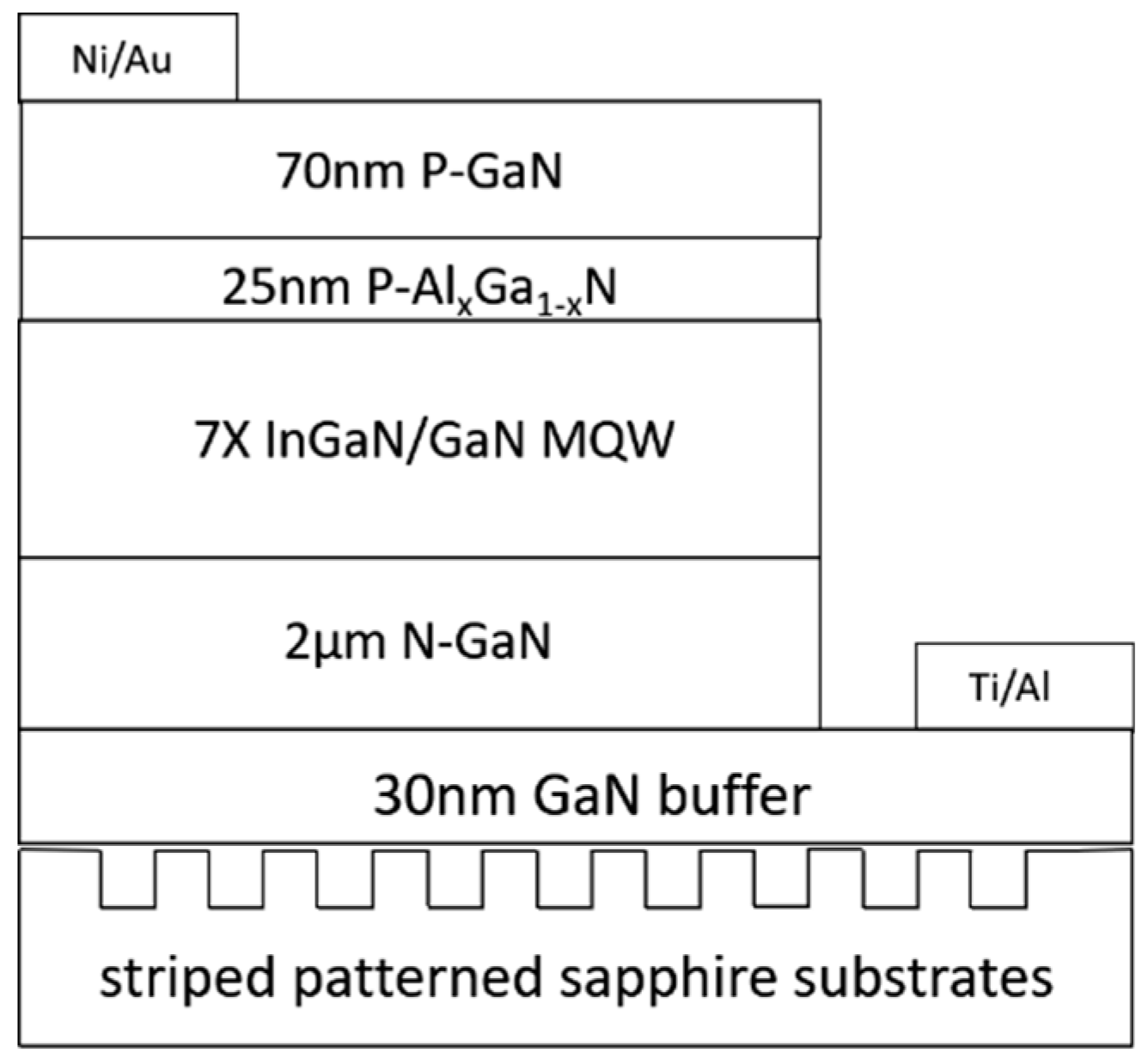
2. Materials and Methods
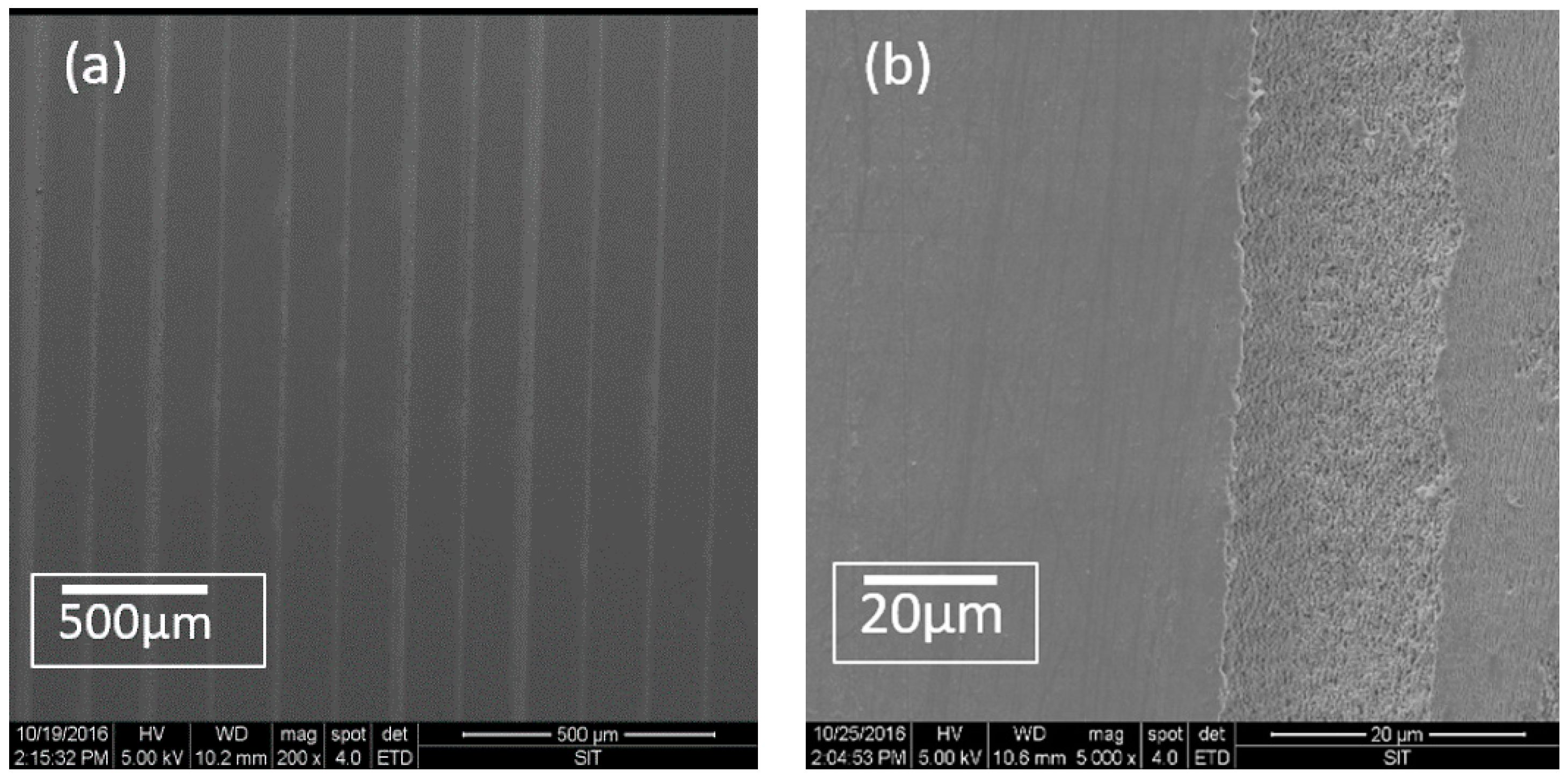
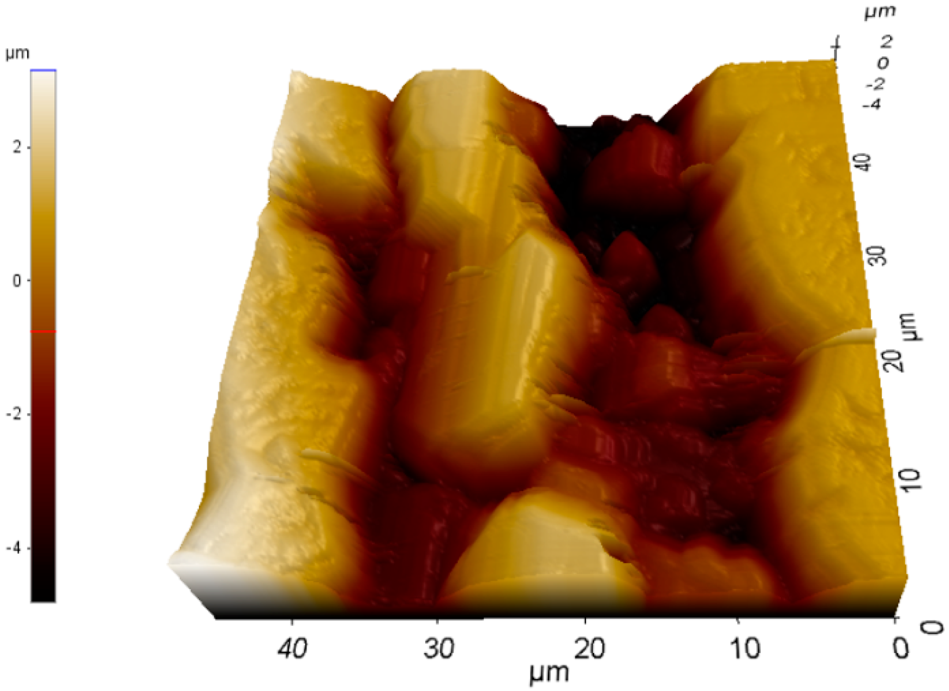
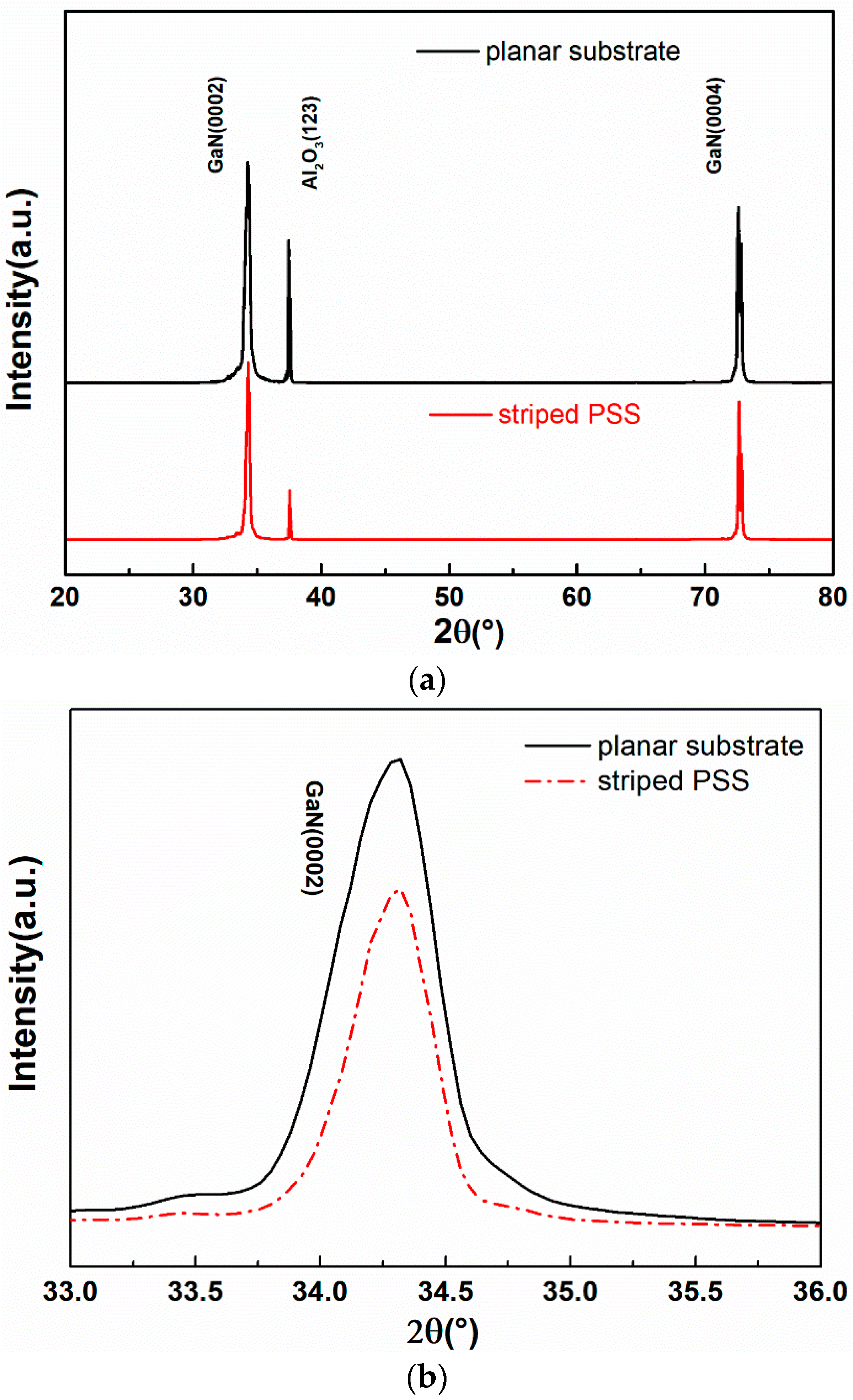
3. Results and Discussion
4. Conclusions
Author Contributions
Funding
Conflicts of Interest
References
- Reed, M.D.; Kryliouk, O.M.; Mastro, M.A.; Anderson, T.J. Growth and characterization of single-crystalline gallium nitride using (100) LiAlO2 substrates. J. Cryst. Growth 2005, 274, 14–20. [Google Scholar] [CrossRef]
- Wang, W.; Yang, W. Epitaxial growth of GaN films on unconventional oxide substrates. J. Mater. Chem. 2014, 2, 9342–9358. [Google Scholar] [CrossRef]
- Le Vaillant, Y.M.; Bisaro, R. Caracterization of AIN buffer layers on (0001)-sapphire substrates. Mater. Sci. Eng. B 1997, 50, 32–37. [Google Scholar] [CrossRef]
- Sakai, A.; Sunakawa, H. Defect structure in selectively grown GaN films with low threading dislocation density. Appl. Phys. Lett. 1997, 71, 2259–2261. [Google Scholar] [CrossRef]
- Nakada, N.; Nakaji, M. Improved characteristics of InGaN multiple-quantum-well light-emitting diode by GaN/AlGaN distributed Bragg reflector grown on sapphire. Appl. Phys. Lett. 2000, 76, 1804–1806. [Google Scholar] [CrossRef]
- Fan, S.; Villeneuve, P.R. Rate-equation analysis of output efficiency and modulation rate of photonic-crystal light-emitting diodes. IEEE J. Quantum Electron. 2002, 36, 1123–1130. [Google Scholar] [CrossRef]
- David, A.; Meier, C. Photonic bands in two-dimensionally patterned multimode GaN waveguides for light extraction. Appl. Phys. Lett. 2005, 87, 101107. [Google Scholar] [CrossRef]
- Na, S.I.; Ha, G.Y. Selective wet etching of p-GaN for efficient GaN-based light-emitting diodes. IEEE Photonics Technol. Lett. 2006, 18, 1512–1514. [Google Scholar] [CrossRef]
- Fujii, T.; Gao, Y. Increase in the extraction efficiency of GaN-based light-emitting diodes via surface roughening. Appl. Phys. Lett. 2004, 84, 855–857. [Google Scholar] [CrossRef]
- Tun, C.J.; Sheu, J.K. Enhanced light output of GaN-based power LEDs with transparent Al-doped ZnO current spreading layer. IEEE Photonics Technol. Lett. 2006, 18, 274–276. [Google Scholar] [CrossRef]
- Lee, K.S.; Kwack, H.S. Spatial correlation between optical properties and defect formation in GaN thin films laterally overgrown on cone-shaped patterned sapphire substrates. J. Appl. Phys. 2010, 107, 103506. [Google Scholar] [CrossRef]
- Tadatomo, K.; Okagawa, H. High Output Power InGaN Ultraviolet Light-Emitting Diodes Fabricated on Patterned Substrates Using Metalorganic Vapor Phase Epitaxy. Jpn. J. Appl. Phys. 2001, 40, L583–L585. [Google Scholar] [CrossRef]
- Chang, S.J.; Lin, Y.C. Nitride-based LEDs fabricated on patterned sapphire substrates. Solid-State Electron. 2003, 47, 1539–1542. [Google Scholar] [CrossRef]
- Lee, J.H.; Oh, J.T. Improvement of luminous intensity of InGaN light emitting diodes grown on hemispherical patterned sapphire. Phys. Status Solidi 2010, 3, 2169–2173. [Google Scholar] [CrossRef]
- Cheng, J.H.; Sermon Wu, Y. Improved crystal quality and performance of GaN-based light-emitting diodes by decreasing the slanted angle of patterned sapphire. Appl. Phys. Lett. 2010, 96, 051109. [Google Scholar] [CrossRef]
- Suihkonen, S.; Ali, M. Patterning of sapphire/GaN substrates. Phys. Status Solidi 2011, 8, 1509–1512. [Google Scholar] [CrossRef]
- Guo, H.; Zhang, X. High-Performance GaN-Based Light-Emitting Diodes on Patterned Sapphire Substrate with a Novel Patterned SiO2/Al2O3 Passivation Layer. Appl. Phys. Express 2013, 6, 2103. [Google Scholar] [CrossRef]
- Yin, S.; Wang, C. Single chip super broadband InGaN/GaN LED enabled by nanostructured substrate. Opt. Express 2014, 22, A1380. [Google Scholar] [CrossRef] [PubMed]
- Hang, D.R.; Chou, M. Optical investigations of non-polar bm{m}- plane InGaN/GaN multiple quantum wells grown on LiAlO2 (100) by using MOVPE. J.-Korean Phys. Soc. 2009, 55, 250. [Google Scholar] [CrossRef]
- Scherrer, P.; Gottingen, N.G.W. Bestimmung der Größe und der inneren Struktur von Kolloidteilchen mittels Röntgenstrahlen. Math. Physik. Kl. 1918, A2, 96–100. [Google Scholar]
- Vajpeyi, A.P.; Tripathy, S. Investigation of optical properties of nanoporous GaN films. Phys. E 2005, 28, 141–149. [Google Scholar] [CrossRef]
- Perlin, P.; Jauberthie-Carillon, C. Raman scattering and X-ray-absorption spectroscopy in gallium nitride under high pressure. Phys. Rev. B 1992, 45, 83–89. [Google Scholar] [CrossRef]
- Tripathy, S.; Chua, S.J. Micro-Raman investigation of strain in GaN and AlxGa1−x N/GaN heterostructures grown on Si(111). J. Appl. Phys. 2002, 92, 3503–3510. [Google Scholar] [CrossRef]
- Zhang, H.; Shao, Y. Growth of high quality GaN on a novel designed bonding-thinned template by HVPE. CrystEngComm 2012, 14, 4777. [Google Scholar] [CrossRef]
- Ponce, F.A.; Gil, B. Group III Nitride Semiconductor Compounds; Oxford University Press: Oxford, UK, 1998; p. 123. [Google Scholar]
- Maruska, H.P.; Hill, D.W. Free-standing non-polar gallium nitride substrates. Opto-Electron. Rev. 2003, 11, 7–17. [Google Scholar]
- Manifacier, J.C.; De Murcia, M. Optical and electrical properties of SnO2 thin films in relation to their stoichiometric deviation and their crystalline structure. Thin Solid Films 1977, 41, 127–135. [Google Scholar] [CrossRef]
- Shinde, V.R.; Gujar, T.P. Mn doped and undoped ZnO films: A comparative structural, optical and electrical properties study. Mater. Chem. Phys. 2006, 96, 326–330. [Google Scholar] [CrossRef]
- Sun, L.; Zou, J. Nonpolar m-plane GaN-based light-emitting diodes on LiAlO2, (100) substrate. J. Mater. Sci. Mater. Electron. 2016, 27, 2049–2053. [Google Scholar] [CrossRef]


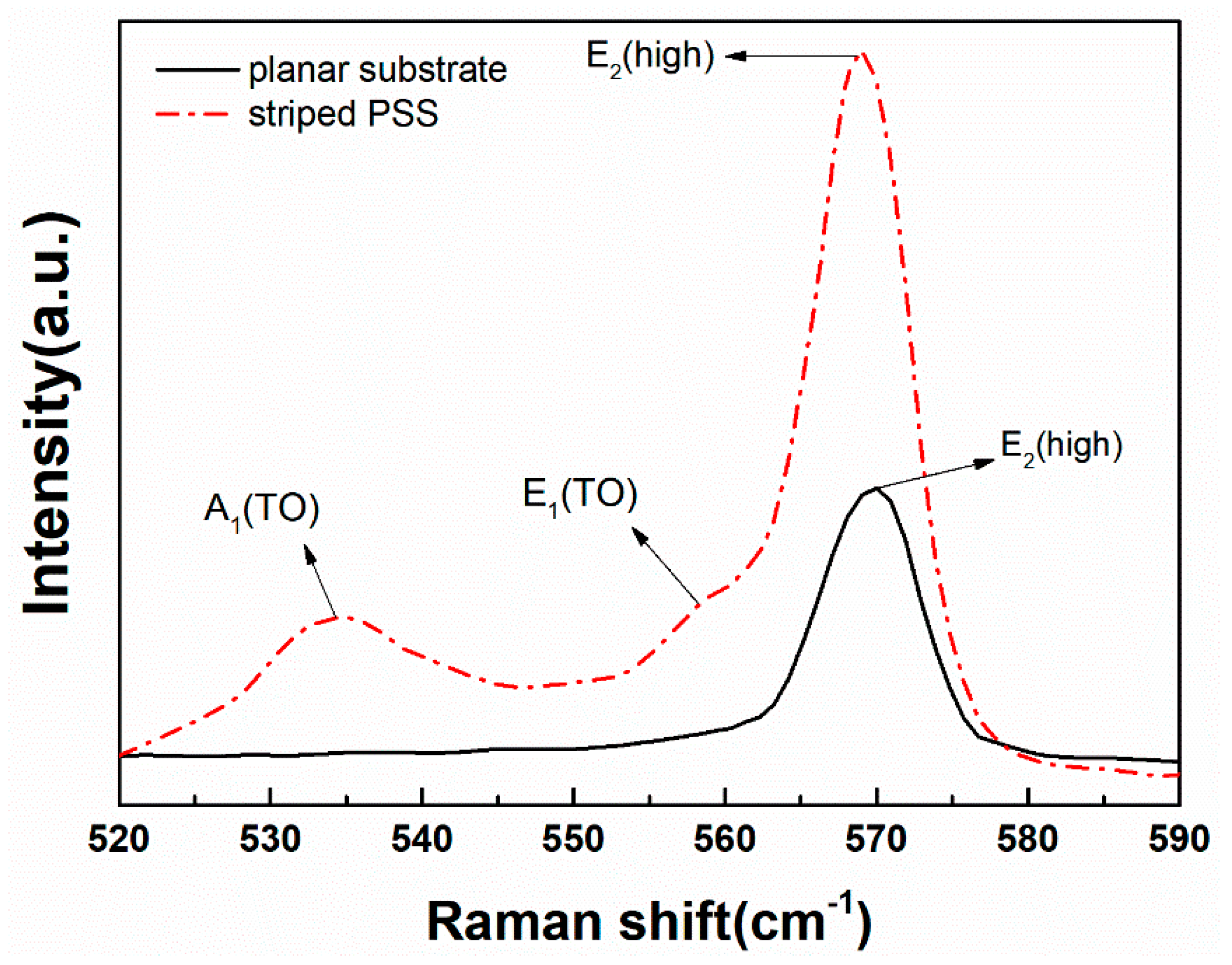
| Samples | E2 Phonon Peak (cm−1) | E2 Phonon FWHM (cm−1) | Compressive Stress (GPa) |
|---|---|---|---|
| planar substrate | 568.8 | 8.1 | 0.45 |
| striped PSS | 569.9 | 6.7 | 0.19 |
© 2018 by the authors. Licensee MDPI, Basel, Switzerland. This article is an open access article distributed under the terms and conditions of the Creative Commons Attribution (CC BY) license (http://creativecommons.org/licenses/by/4.0/).
Share and Cite
Xu, Y.; Zou, J.; Lin, X.; Wu, W.; Li, W.; Yang, B.; Shi, M. Quality-Improved GaN Epitaxial Layers Grown on Striped Patterned Sapphire Substrates Ablated by Femtosecond Laser. Appl. Sci. 2018, 8, 1842. https://doi.org/10.3390/app8101842
Xu Y, Zou J, Lin X, Wu W, Li W, Yang B, Shi M. Quality-Improved GaN Epitaxial Layers Grown on Striped Patterned Sapphire Substrates Ablated by Femtosecond Laser. Applied Sciences. 2018; 8(10):1842. https://doi.org/10.3390/app8101842
Chicago/Turabian StyleXu, Yichao, Jun Zou, Xiaoyan Lin, Wenjuan Wu, Wenbo Li, Bobo Yang, and Mingming Shi. 2018. "Quality-Improved GaN Epitaxial Layers Grown on Striped Patterned Sapphire Substrates Ablated by Femtosecond Laser" Applied Sciences 8, no. 10: 1842. https://doi.org/10.3390/app8101842
APA StyleXu, Y., Zou, J., Lin, X., Wu, W., Li, W., Yang, B., & Shi, M. (2018). Quality-Improved GaN Epitaxial Layers Grown on Striped Patterned Sapphire Substrates Ablated by Femtosecond Laser. Applied Sciences, 8(10), 1842. https://doi.org/10.3390/app8101842