
Self-Assembly of High Density of Triangular Silver Nanoplate Films Promoted by 3-Aminopropyltrimethoxysilane

Abstract
:
1. Introduction
2. Experimental Section
2.1. Chemicals
2.2. Synthesis and Fabrication of Monolayer Triangular Silver Nanoplate Thin Film
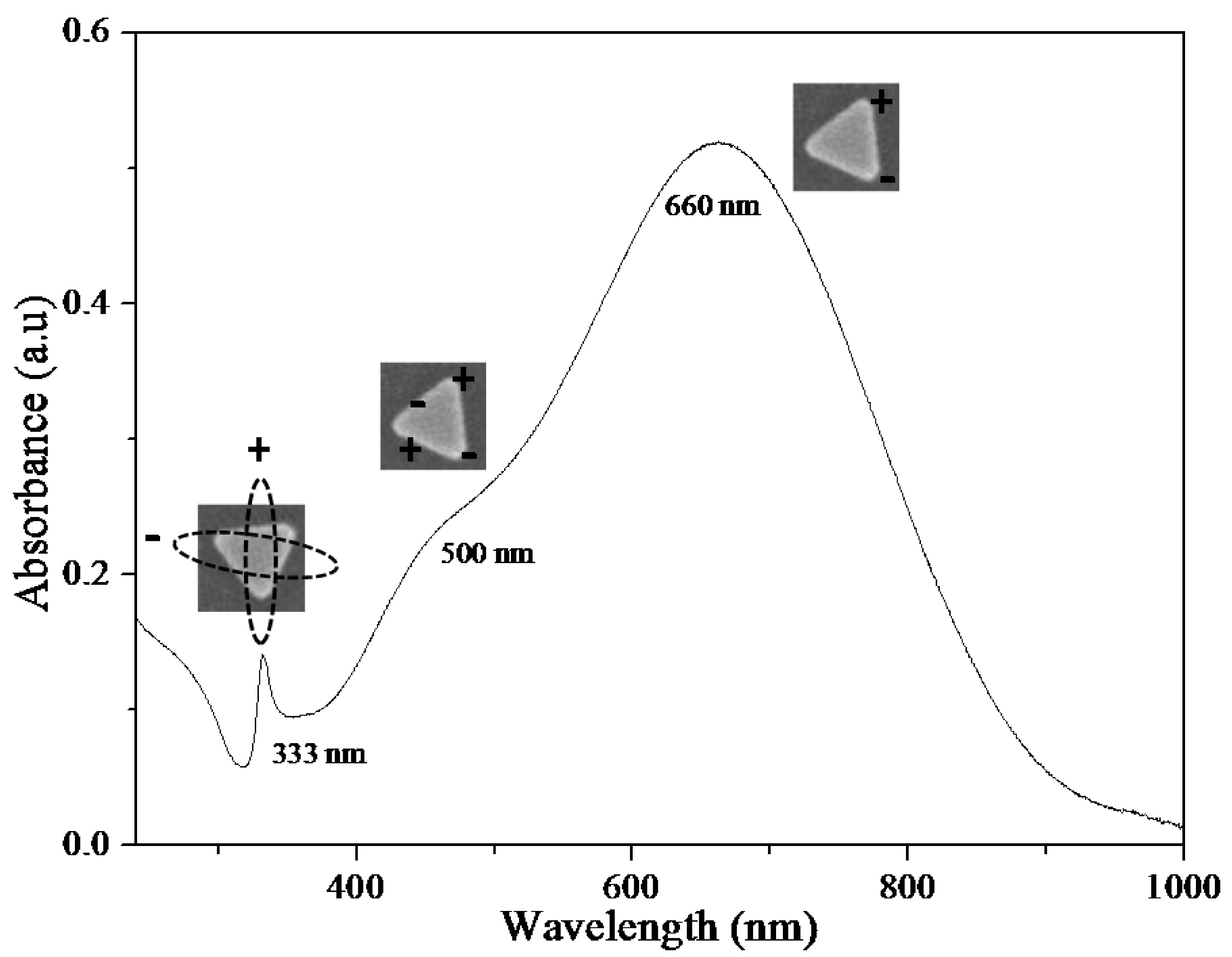
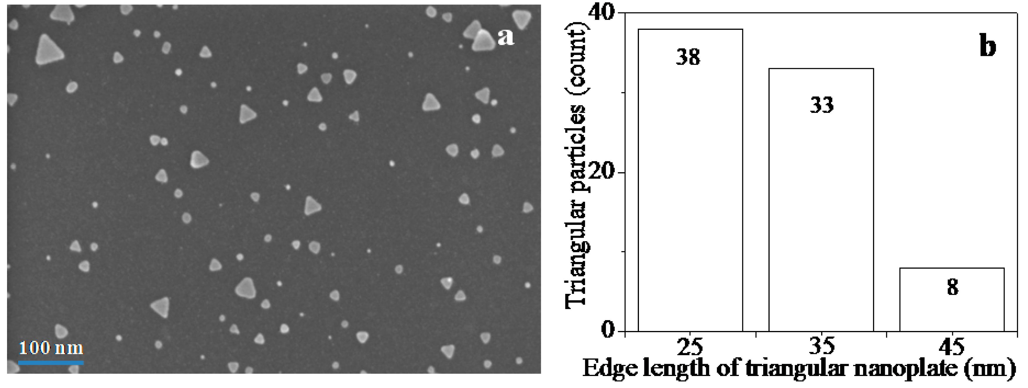
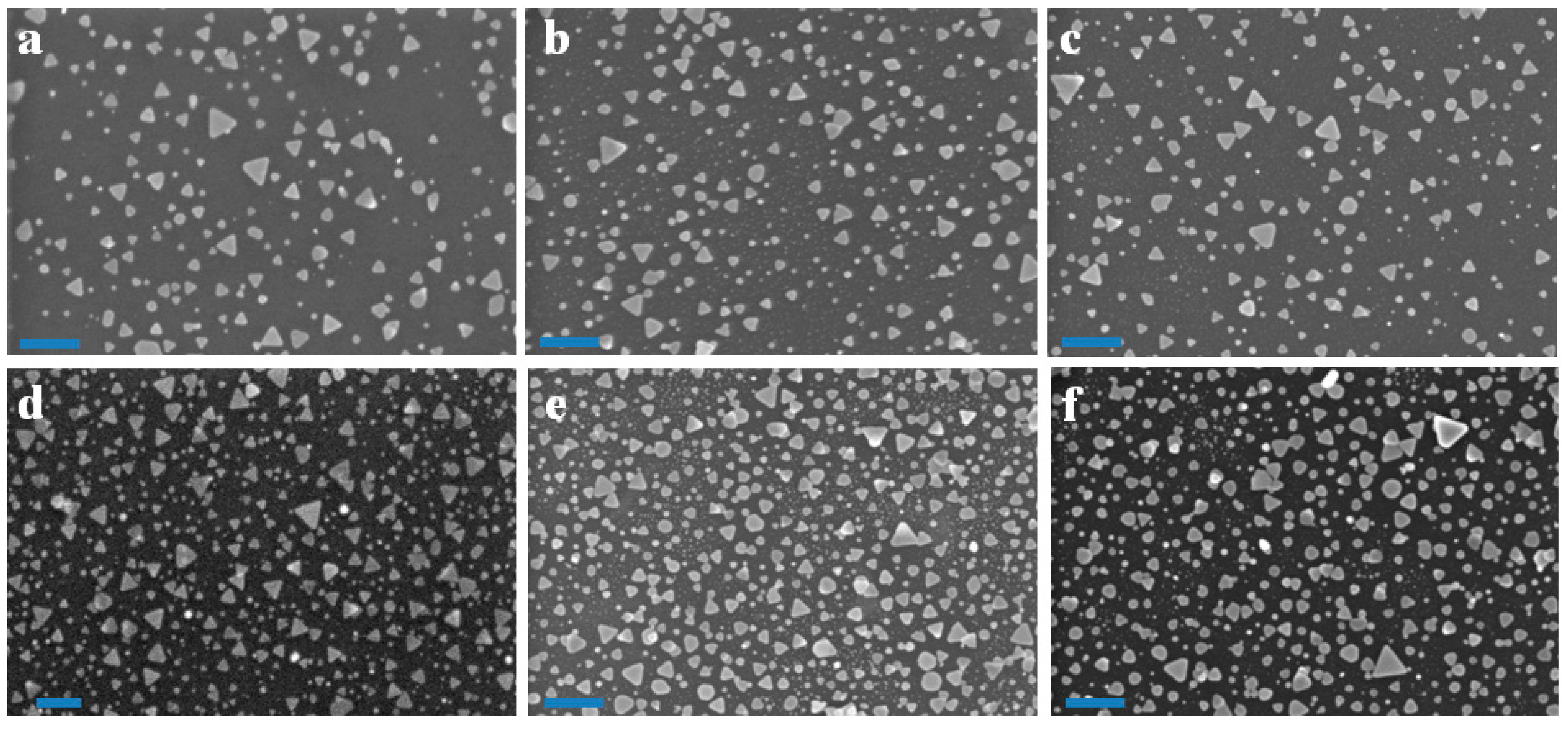
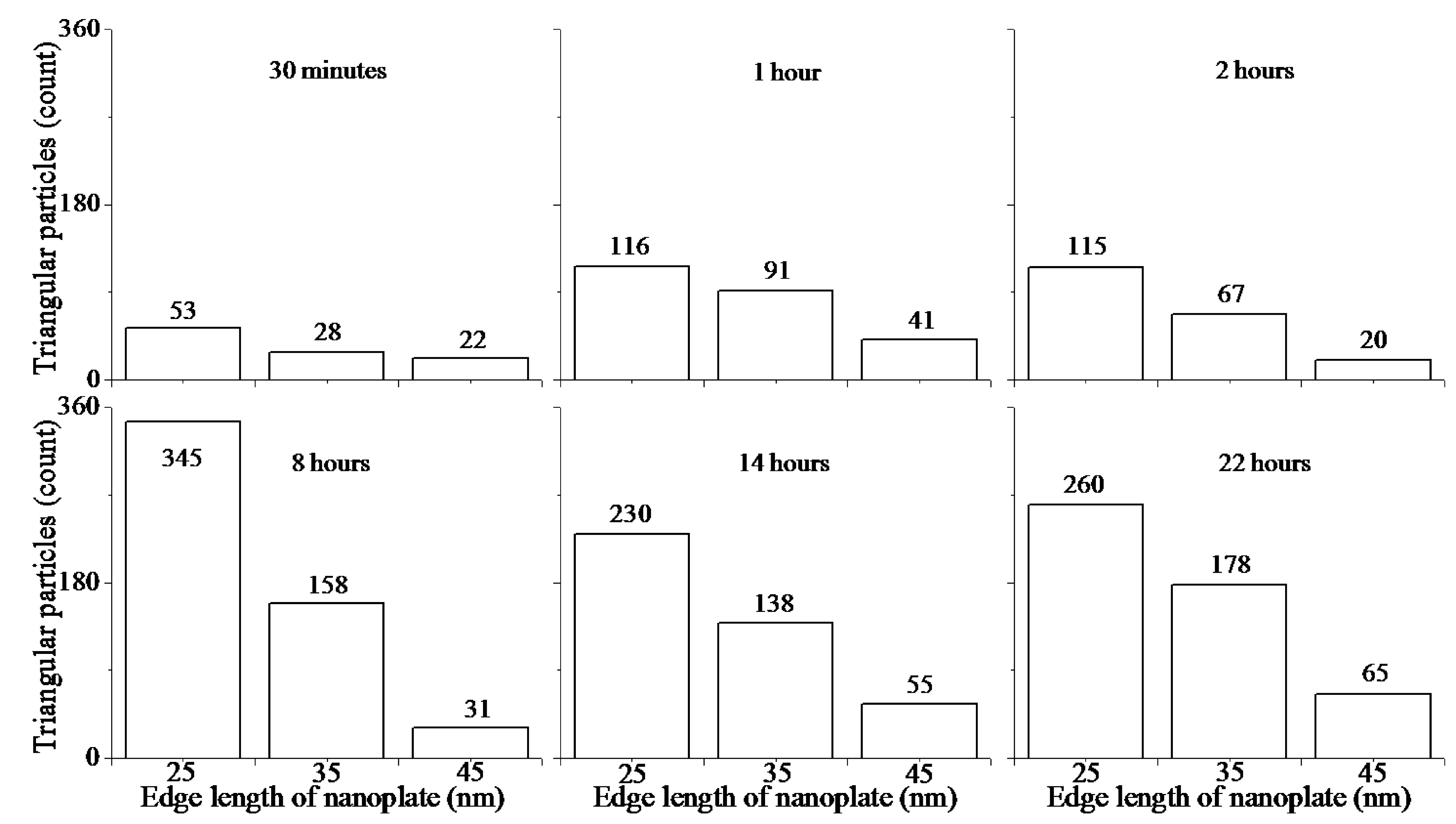
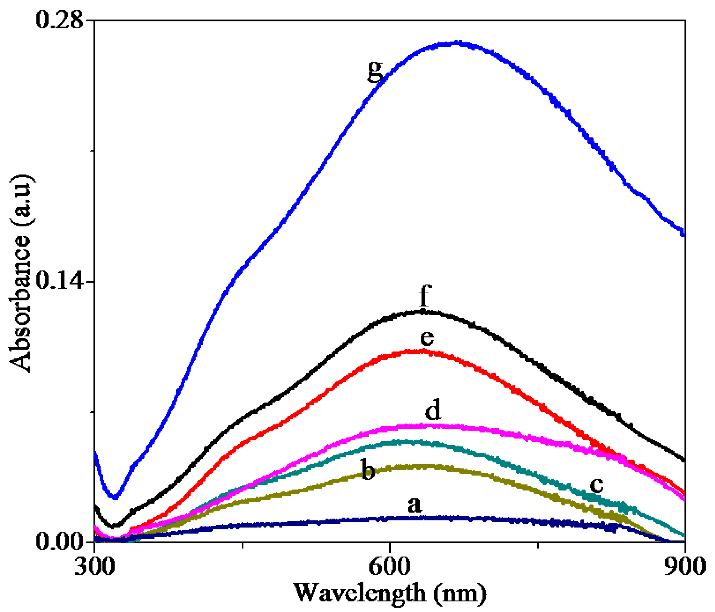
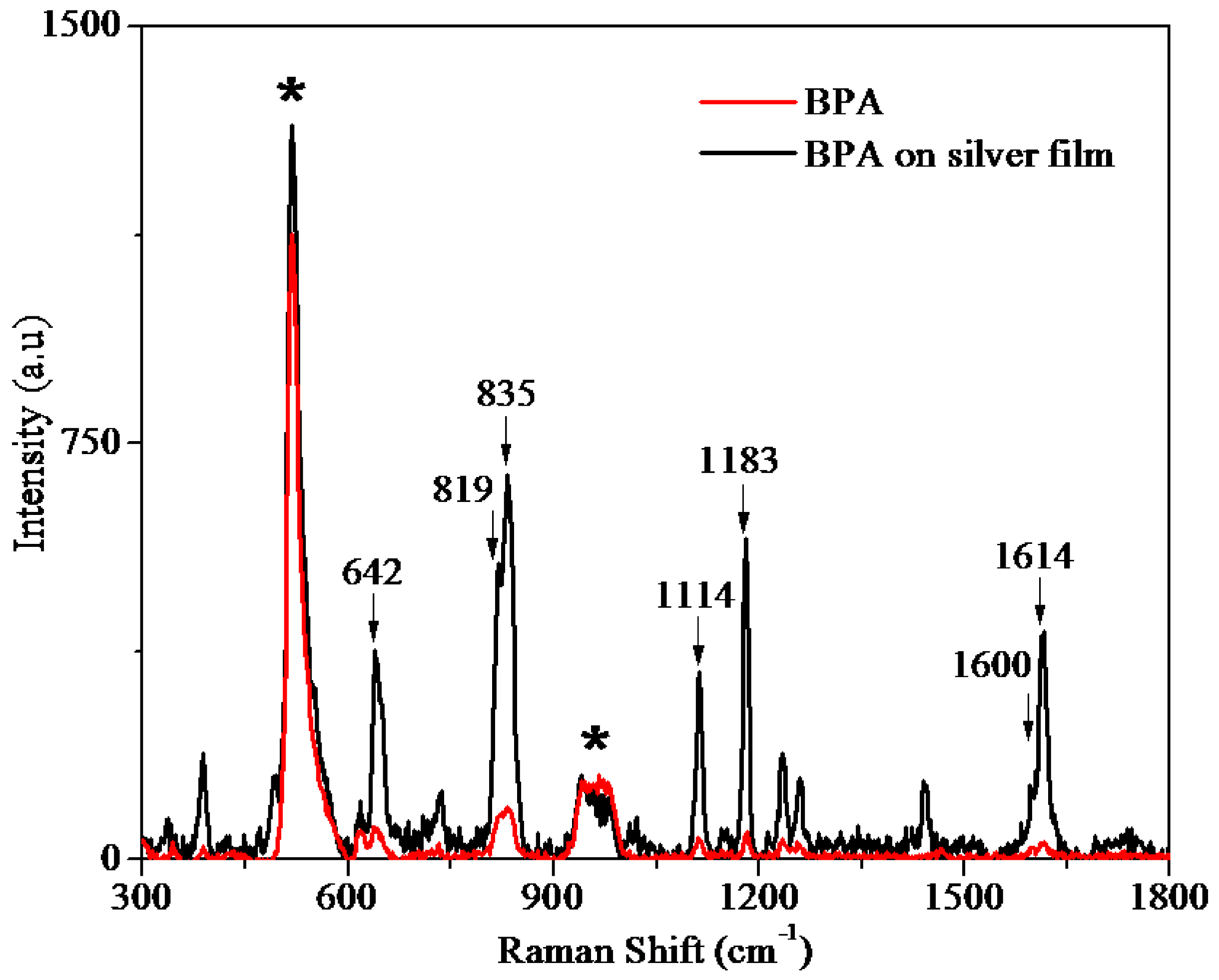
3. Results and Discussion


| Exposure Times | Edge Length of Nanoplates (nm) | Coverage of Nanoplates on the Surfaces (Counts/µm) |
|---|---|---|
| 15 min | 25.05 ± 7.37 | 79 |
| 30 min | 25.59 ± 9.72 | 103 |
| 1 h | 26.21 ± 8.40 | 248 |
| 2 h | 24.37 ± 7.37 | 202 |
| 8 h | 27.47 ± 6.68 | 534 |
| 14 h | 25.24 ± 7.49 | 423 |
| 22 h | 25.11 ± 7.68 | 503 |

4. Conclusions
Supplementary Files
Supplementary File 1Acknowledgments
Author Contributions
Conflicts of Interest
References
- Zeng, J.; Zheng, Y.; Rycenga, M.; Tao, J.; Li, Z.Y.; Zhang, Q.; Zhu, Y.; Xia, Y. Controlling the shapes of silver nanocrystals with different capping agents. J. Am. Chem. Soc. 2010, 132, 8552–8553. [Google Scholar] [CrossRef] [PubMed]
- Jin, M.; He, G.; Zhang, H.; Zeng, J.; Xie, Z.; Xia, Y. Shape-controlled synthesis of copper nanocrystals in an aqueous solution with glucose as a reducing agent and hexadecylamine as a capping agent. Angew. Chem. Int. Edit. 2011, 50, 10560–10564. [Google Scholar] [CrossRef] [PubMed]
- Tsuji, M.; Gomi, S.; Maeda, Y.; Matsunaga, M.; Hikino, S.; Uto, K.; Tsuji, T.; Kawazumi, H. Rapid transformation from sperical nanoparticles, nanorods, cubes, or bipyramids to triangular prisms of silver with PVP, Citrate, and H2O2. Langmuir 2012, 28, 8845–8861. [Google Scholar] [CrossRef] [PubMed]
- Taleb, A.; Petit, C.; Pileni, M.P. Synthesis of highly monodisperse silver nanoparticles from AOT reverse micelles: A way to 2D and 3D self-organization. Chem. Mater. 1997, 9, 950–959. [Google Scholar] [CrossRef]
- Krutyakov, Y.A.; Kudrinskiy, A.A.; Olenin, A.Y.; Lisichkin, G.V. Synthesis and properties of silver nanoparticles: Advances and prospects. Russ. Chem. Rev. 2008, 77, 233–257. [Google Scholar] [CrossRef]
- Sun, Y.; Gates, B.; Mayers, B.; Xia, Y. Crystalline silver nanowires by soft solution processing. Nano Lett. 2002, 2, 165–168. [Google Scholar] [CrossRef]
- Caswell, K.K.; Bender, C.M.; Murphy, C.J. Seedless, surfactantless wet chemical synthesis of silver nanowires. Nano Lett. 2003, 3, 667–669. [Google Scholar] [CrossRef]
- Ledwith, D.M.; Aine, M.W.; John, M.K. A Rapid, straight-forward method for controlling the morphology of stable silver nanoparticles. J. Mater. Chem. 2007, 17, 2459–2464. [Google Scholar] [CrossRef]
- Lim, G.H.; Han, I.; Yu, T.; Lim, B. Aqueous-phase synthesis of silver nanoplate: Enhancing lateral growth via a heat-up process. Chem. Phys. Lett. 2013, 568, 135–139. [Google Scholar] [CrossRef]
- Zhang, Q.; Huang, C.Z.; Ling, J.; Li, Y.F. Silver nanocubes formed on ATP-mediated nafion film and a visual method for formaldehyde. J. Chem. Phys. B 2008, 112, 16990–16994. [Google Scholar] [CrossRef] [PubMed]
- Guo, S.; Dong, S.; Wang, E. Rectangular silver nanorods: Controlled preparation, liquid-liquid interface assembly, and application in surface-enhanced Raman scattering. Cryst. Growth Des. 2009, 9, 372–377. [Google Scholar] [CrossRef]
- Kelly, K.L.; Coronado, E.; Zhao, L.L.; Schatz, G.C. The optical properties of metal nanoparticles: The influence of size, shape, and dielectric environment. J. Chem. Phys. B 2003, 107, 668–667. [Google Scholar] [CrossRef]
- Zhang, X.Y.; Hu, A.; Zhang, T.; Lei, W.; Xue, X.J.; Zhou, Y.; Duley, W.W. Self-assembly of large-scale and ultrathin silver nanoplate films with tunable plasmon resonance properties. ACS Nano 2011, 5, 9082–9092. [Google Scholar] [CrossRef] [PubMed]
- Li, N.; Zhang, Q.; Quinlivan, S.; Goebl, J.; Gan, Y.; Yin, Y. H2o2-aided seed-mediated synthesis of silver nanoplates with improved yield and efficiency. ChemPhysChem 2012, 13, 2526–2530. [Google Scholar] [CrossRef] [PubMed]
- Pastoriza-Santos, I.; Liz-Marzán, L.M. Colloidal silver nanoplates. State of the art and future challenges. J. Mater. Chem. 2008, 18, 1724–1737. [Google Scholar] [CrossRef]
- Si, G.; Shi, W.; Li, K.; Ma, Z. Synthesis of PSS-capped triangular silver nanoplates with tunable SPR. Colloids Surf. A 2011, 380, 257–260. [Google Scholar] [CrossRef]
- Zhang, J.; Sun, Y.; Zhang, H.; Xu, B.; Zhang, H.; Song, D. Preparation and application of triangular silver nanoplates/chitosan composite in surface plasmon resonance biosensing. Anal. Chim. Acta 2013, 769, 114–120. [Google Scholar] [CrossRef] [PubMed]
- Brandon, M.P.; Ledwith, D.M.; Kelly, J.M. Preparation of saline-stable, silica-coated triangular silver nanoplates of use for optical sensing. J. Colloid Interf. Sci. 2014, 415, 77–84. [Google Scholar] [CrossRef] [PubMed]
- Folmar, M.; Shtoyko, T.; Fudala, R.; Akopova, I.; Gryczynski, Z.; Raut, S.; Gryczynski, I. Metal enhanced fluorescence of Me-ADOTA Cl dye by silver triangular nanoprisms on a gold film. Chem. Phys. Lett. 2012, 531, 126–131. [Google Scholar] [CrossRef]
- Yan, B.; Thubagere, A.; Premasiri, W.R.; Ziegler, L.; Negro, L.D.; Reinhard, B.M. Engineered SERS substrates with multiscale signal enhancement: Nanoparticle cluster arrays. ACS Nano 2009, 3, 1190–1202. [Google Scholar] [CrossRef] [PubMed]
- Zeng, J.; Xia, X.; Rycenga, M.; Henneghan, P.; Li, Q.; Xia, Y. Successive deposition of silver on silver nanoplates: Lateral vs. vertical growth. Angew. Chem. Int. Edit. 2011, 50, 244–249. [Google Scholar] [CrossRef] [PubMed]
- Ramanauskaite, L.; Snitka, V. Surface enhanced Raman spectroscopy of l-alanyl-l-tryptophan dipeptide adsorbed on Si substrate decorated with triangular silver nanoplates. Chem. Phys. Lett. 2015, 623, 46–50. [Google Scholar] [CrossRef]
- Leopold, N.; Lendl, B. A new method for fast preparation of highly surface-enhanced Raman scattering (SERS) active silver colloids at room temperature by reduction of silver nitrate with hydroxylamine hydrochloride. J. Chem. Phys. B 2003, 107, 5723–5727. [Google Scholar] [CrossRef]
- Liu, J.; White, I.; Devoe, D.L. Nanoparticles-funtionalized porous polymer monolith detection elements for surface-enhanced Raman scattering. Anal. Chem. 2011, 83, 2119–2124. [Google Scholar] [CrossRef] [PubMed]
- Doak, J.; Gupta, R.K.; Manivannan, K.; Ghosh, K.; Kahol, P.K. Effect of particle size distributions on absorbance spectra of gold nanoparticles. Phys. E 2010, 42, 1605–1609. [Google Scholar] [CrossRef]
- Khan, M.A.M.; Kumar, S.; Ahamed, M.; Alrokayan, S.A.; Alsalhi, M.S. Structural and thermal studies of silver nanoparticles and electrical transport study of their thin films. Nanoscale Res. Lett. 2011, 6, 434–441. [Google Scholar] [CrossRef] [PubMed]
- Aslan, K.; Lakowicz, J.R.; Geddes, C.D. Rapid deposition of triangular silver nanoplates on planar surfaces: Application to metal-enhanced fluorescence. J. Chem. Phys. B 2005, 109, 6247–6251. [Google Scholar] [CrossRef] [PubMed]
- Gooding, J.J.; Ciampi, S. The molecular level modification of surfaces: From self-assembled monolayers to complex molecular assemblies. Chem. Soc. Rev. 2011, 40, 2704–2718. [Google Scholar] [CrossRef] [PubMed]
- Zhu, M.; Lerum, M.Z.; Chen, W. How to prepare reproducible, homogeneous, and hydrolytically stable aminosilane-derived layers on silica. Langmuir 2012, 28, 416–423. [Google Scholar] [CrossRef] [PubMed]
- Enders, D.; Nagao, T.; Pucci, A.; Nakayama, T. Reversible adsorption of Au nanoparticles on SiO2/Si: An in situ ATR-IR study. Surf. Sci. 2006, 600, 71–75. [Google Scholar] [CrossRef]
- Kooij, E.S.; Brouwer, E.A.M.; Wormeester, H.; Poelsema, B. Ionic strength mediated self-organization of gold nanocrystals: An AFM study. Langmuir 2002, 18, 7677–7682. [Google Scholar] [CrossRef]
- Zhang, Q.; Li, N.; Goebl, J.; Lu, Z.; Yin, Y. A systematic study of the synthesis of silver nanoplates: Is citrate a “Magic” Reagent? J. Am. Chem. Soc. 2011, 133, 18931–18939. [Google Scholar] [CrossRef] [PubMed]
- Xia, X.; Zeng, J.; Zhang, Q.; Moran, C.H.; Xia, Y. Recent developments in shape-controlled synthesis of silver nanocrystals. J. Chem. Phys. C 2012, 116, 21647–21656. [Google Scholar] [CrossRef] [PubMed]
- Jin, R.; Cao, Y.C.; Hao, E.; Metraux, G.S.; Schatz, G.C.; Mirkin, C.A. Controlling anisotropic nanoparticle growth through plasmon excitation. Nature 2003, 425, 487–490. [Google Scholar] [CrossRef] [PubMed]
- Yi, Z.; Zhang, J.; He, H.; Xu, X.; Luo, B.; Li, X.; Li, K.; Niu, G.; Tan, X.; Luo, J.; et al. Convenient synthesis of silver nanoplates with adjustable size through seed mediated growth approach. Trans. Nonferrous Met. Soc. China 2012, 22, 865–872. [Google Scholar] [CrossRef]
- Howarter, J.A.; Youngblood, J.P. Optimization of silica silanization by 3-aminopropyltriethoxysilane. Langmuir 2006, 22, 11142–11147. [Google Scholar] [CrossRef] [PubMed]
- Klug, J.; Pérez, L.A.; Coronado, E.A.; Lacconi, G.I. Chemical and electrochemical oxidation of silicon surfaces functionalized with APTES: The role of surface roughness in the AuNPs anchoring kinetics. J. Chem. Phys. C 2013, 117, 11317–11327. [Google Scholar] [CrossRef]
- Scarpettini, A.F.; Bragas, A.V. Coverage and aggregation of gold nanoparticles on silanized glasses. Langmuir 2010, 26, 15948–15953. [Google Scholar] [CrossRef] [PubMed]
- Wei, H.; Eilers, H. From silver nanoparticles to thin films: Evolution of microstructures and electrical conduction on glass substrates. J. Phys. Chem. Solids 2009, 70, 459–465. [Google Scholar] [CrossRef]
- Yao, W.; Wang, S.; Wang, H. Method for Detecting BPA by Surface Enhanced Raman Spectroscopy; Patent Application Publication: Alexandria, VA, USA, 2012. [Google Scholar]
© 2015 by the authors; licensee MDPI, Basel, Switzerland. This article is an open access article distributed under the terms and conditions of the Creative Commons Attribution license (http://creativecommons.org/licenses/by/4.0/).
Share and Cite
Bakar, N.A.; Shapter, J.G.; Salleh, M.M.; Umar, A.A. Self-Assembly of High Density of Triangular Silver Nanoplate Films Promoted by 3-Aminopropyltrimethoxysilane. Appl. Sci. 2015, 5, 209-221. https://doi.org/10.3390/app5030209
Bakar NA, Shapter JG, Salleh MM, Umar AA. Self-Assembly of High Density of Triangular Silver Nanoplate Films Promoted by 3-Aminopropyltrimethoxysilane. Applied Sciences. 2015; 5(3):209-221. https://doi.org/10.3390/app5030209
Chicago/Turabian StyleBakar, Norhayati Abu, Joe George Shapter, Muhamad Mat Salleh, and Akrajas Ali Umar. 2015. "Self-Assembly of High Density of Triangular Silver Nanoplate Films Promoted by 3-Aminopropyltrimethoxysilane" Applied Sciences 5, no. 3: 209-221. https://doi.org/10.3390/app5030209
APA StyleBakar, N. A., Shapter, J. G., Salleh, M. M., & Umar, A. A. (2015). Self-Assembly of High Density of Triangular Silver Nanoplate Films Promoted by 3-Aminopropyltrimethoxysilane. Applied Sciences, 5(3), 209-221. https://doi.org/10.3390/app5030209