Article

Optimization of Sample Preparation for Transmission Electron Microscopy Based on Several Nanomaterial Cases


1
Anhui Province Key Laboratory of Intelligent Car Wire-Controlled Chassis System, Anhui Polytechnic University, Wuhu 241000, China
2
School of Integrated Circuits, Anhui Polytechnic University, Wuhu 241000, China
3
Wuhan National High Magnetic Field Center, Huazhong University of Science and Technology, Wuhan 430074, China
4
College of Biological and Food Engineering, Anhui Polytechnic University, Wuhu 241000, China
5
Modern Technology Center, Anhui Polytechnic University, Wuhu 241000, China
*
Author to whom correspondence should be addressed.
Appl. Sci. 2026, 16(9), 4335; https://doi.org/10.3390/app16094335
Submission received: 26 March 2026 / Revised: 17 April 2026 / Accepted: 22 April 2026 / Published: 29 April 2026

Abstract

Transmission electron microscopy (TEM) is an essential technique for characterizing nanomaterials. However, specimen preparation, which is a critical factor affecting image quality, remains a practical challenge. Focusing on nanopowders used in materials and chemical science, this article employs case studies to analyze the key steps in TEM specimen preparation. Carbon support films (CSFs) are essential tools for specimen preparation, and this study introduces several commonly used, cost-effective options, including conventional CSFs, conventional holey CSFs, ultrathin holey CSFs, and double-grid support films. We characterize their structural and morphological characteristics and evaluate their suitability for different types of samples. Several representative case studies of nanopowders, spanning from zero-dimensional (0D) to one-dimensional (1D) and two-dimensional (2D) materials, are used to illustrate tailored specimen preparation approaches, which serve as practical references for researchers conducting TEM characterization. These findings facilitate higher image reliability and experimental efficiency, thereby providing critical support for advancing fundamental exploration and frontier innovation in nanomaterial science.

1. Introduction

TEM uses an electron beam with an extremely short wavelength (2.51 pm at 200 kV) as the illumination source. According to the Rayleigh criterion [1], a shorter wavelength enables higher resolution. With modern aberration correction, the resolution is routinely pushed below 0.1 nm, enabling true atomic-scale imaging. Such exceptional spatial resolution endows TEM with unique advantages across multiple disciplines: in material science, it allows direct imaging of defects like grain boundaries and dislocations at the atomic scale [2]; in life science, it has become indispensable for high-resolution structure determination of proteins and macromolecular complexes [3]; and in chemistry science, TEM is widely used to directly visualize the phase composition and microstructure of active components, establishing structure–functional performance relationships [4].
However, TEM imaging quality not only depends on the instrument’s aberration but is also critically constrained by the specimen preparation quality. This is particularly true for low-dimensional nanopowder (with at least one dimension below 100 nm); particle agglomeration obscures the identification of intrinsic structural features (e.g., particle size and morphology) of individual nanoparticles and hinders high-resolution structural analysis, leading to misinterpretation of microstructure–property relationships [5]. Surface contamination from solvents or ambient exposure, such as residual hydrocarbons, can lead to the formation of amorphous carbonaceous deposition under EB irradiation [6]. This deposited layer not only causes significant image drift but also degrades image contrast, often to the point where atomic-scale lattice fringes become indistinguishable. In addition, the carbon support film used to hold the specimen also has a significant impact on imaging quality. For instance, a thick carbon film can increase inelastic scattering and generate strong background noise [7], severely degrading image contrast, especially for low-contrast specimens. Nanomaterials vary widely in composition and physical state, differing in hydrophilicity, stability, and mechanical flexibility. Consequently, a wide range of preparation methods has been developed, each with distinct applicability and inherent limitations. No universal method fits all cases; therefore, the optimal strategy depends on the specific nanomaterial and the analytical requirements. Developing TEM sample preparation methods that can preserve the intrinsic structure of nanomaterials during both preparation and characterization, and that can thus faithfully reveal their structural features, remains a major challenge. Researchers have recently advanced the TEM specimen preparation methodology. Using the continuous aerosol dispersion system with high-pressure discharge developed by Yuan et al., the median diameter of TiO2 nanoparticle agglomerates was reduced from approximately 169 nm to 24.5 nm [8]. For contamination mitigation, plasma cleaning has proven effective in removing hydrocarbon contaminants from specimen surfaces prior to imaging. Armbruster et al. demonstrated that oxygen plasma cleaning achieves removal rates of up to 0.75 nm/s with minimal damage to carbon-based support films [9]. To overcome the high background noise introduced by the thickness of conventional amorphous carbon films, atomic-thick graphene carbon films have been developed. Silicon nitride (SiN) grids offer a carbon-free substrate that eliminates carbon background interference in EDX analysis, and their nanoporous structure enables cleaner particle imaging, free from background disturbance.
Focusing on non-magnetic nanopowder in materials and chemistry science, this work first investigates the physical characteristics of support films (e.g., layered structure, the sizes of grid hole or micropores, film thickness, and their corresponding background noise levels) and analyzes their application suitability. Then, the critical steps in TEM sample preparation process are analyzed. By integrating optimized preparation steps with appropriate support film selection, this work conducts several case studies on nanopowders from different dimensions, such as zero-dimensional (0D) quantum dots [10], one-dimensional (1D) nanowires [11], and two-dimensional (2D) nanosheets [12]. This work thereby illustrates a practical pathway for TEM specimen preparation of such nanopowders, offering a methodological reference for achieving reliable, high-quality TEM imaging.

2. Materials and Methods

Anhydrous ethanol (99.7%), polyethylene glycol (PEG-4000) and polyvinylpyrrolidone (PVP K30) were obtained from Sinopharm Chemical Reagent Co., Ltd. (Shanghai, China). SiO2 nanoparticles were prepared by a sol–gel process based on the Stöber method [13]. ZnO nanocrystals were synthesized by the sol–gel method [14]. Ga2O3 nanoparticles were prepared by the high-temperature thermal decomposition method [15]. The polyurethane-dextran fibers were fabricated by electrospinning. TiO2 nanofibers decorated with BiOCl nanosheets were obtained according to the method reported by Kexin Wang et al. [16]. MXene nanosheets were prepared by etching Ti3AlC2 MAX powder with LiF and HCl. Carbon support films (hereafter referred to as CSF) including conventional CSFs, conventional holey CSFs, ultrathin holey CSFs and double-grid support films were acquired from Zhongjingkeyi Technology Co., Ltd. (Beijing, China).
Deagglomeration of the nanopowder was performed using an ultrasonic processor (180 W, 28 kHz). The organic contaminant on the TEM sample was cleaned using a UV-ozone cleaner (Zonetem II, Zon-2020, Sanyu Co., Ltd., Hitachi Ota, Japan). Optical images were acquired using high-precision optical image measuring instrument (KSY, FH2010-3D, Suzhou, China). All TEM, high-resolution TEM (HRTEM), and scanning transmission electron microscopy (STEM) imaging, combined with energy-dispersive X-ray spectroscopy (EDS) and high-angle annular dark-field (HAADF) imaging, were performed using a TEM (Thermo Fisher Scientific, Talos F200S G2, Waltham, MA, USA) operated at 200 kV. Microstructural analysis of the CSFs was performed with a high-resolution scanning electron microscope (SEM) (Hitachi, SU8600, Tokyo, Japan). The zeta potential and average size distribution of dispersed particles were analyzed by using an analyzer (Zetasizer Nano ZS90, Malvern Panalytical, Malvern, UK).
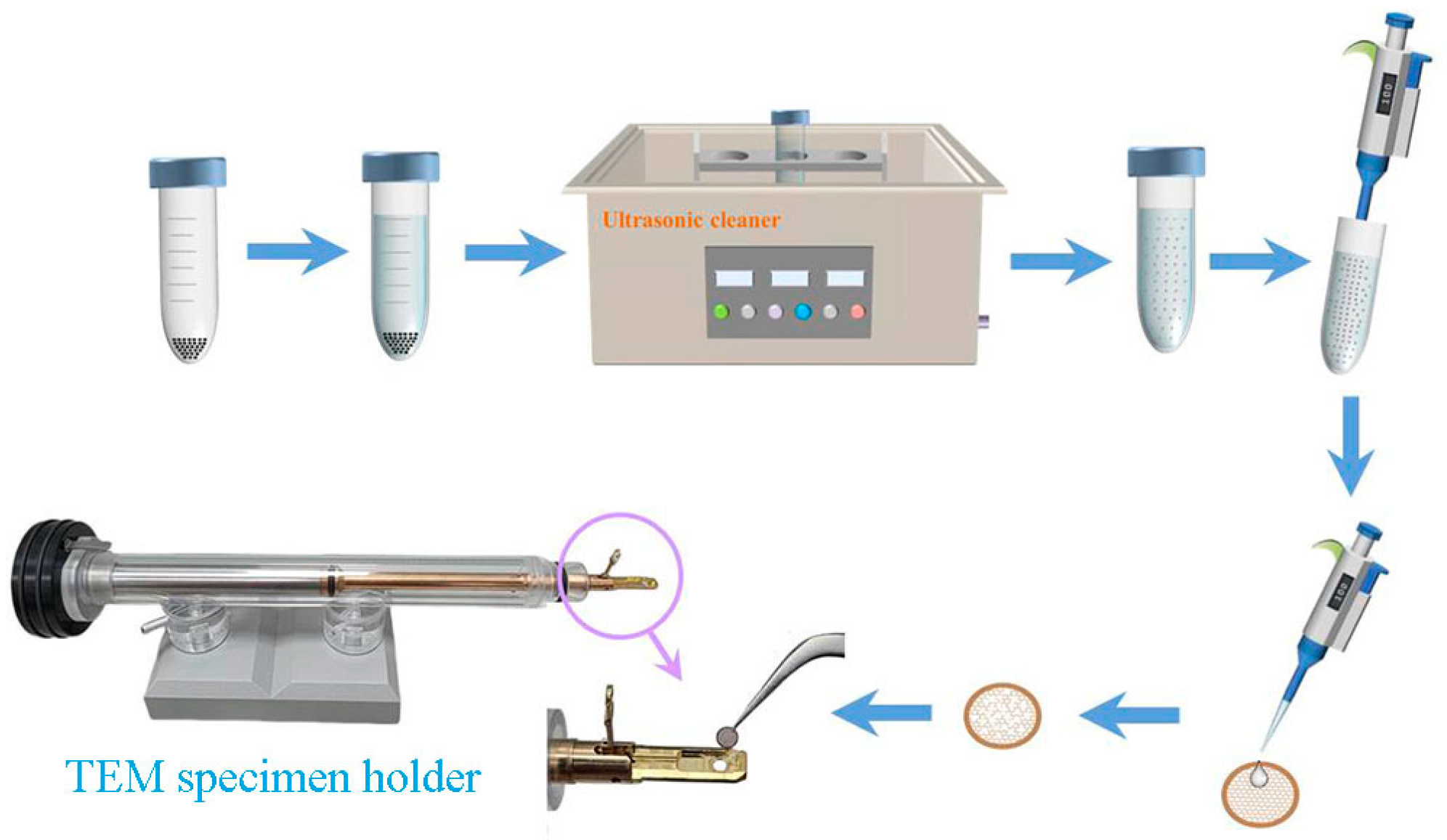
The conventional TEM sample preparation procedure for non-magnetic nanopowder is shown in Figure 1. A small quantity of the powder was ultrasonically dispersed in a solvent (e.g., anhydrous ethanol, deionized water, or acetone, etc.) for 15 min. The dispersed solution was then dropped onto a CSF and dried either under vacuum or in air at ambient temperature. The CSF was carefully placed into the sample pool of the TEM specimen holder.

3. Results and Discussions

3.1. Carbon Support Films

In TEM specimen preparation, the support grids serve not only as a mechanical substrate for holding nanomaterials but also as a key determinant of imaging quality. Its film’s chemical composition, thickness, pore size, and layered structure collectively influence background noise, image contrast, or the mechanical stability of the specimen, making the selection of an appropriate support grid essential for obtaining clear, artifact-free images. Currently, a wide variety of support grids are commercially available, including graphene, silicon nitride support grids, and various amorphous CSFs (e.g., conventional CSF, conventional holey CSF, ultrathin holey CSF, double-layer support film, etc.). Among them, graphene grid, with its ultra-electron-transparent nature, is particularly suitable for cryo-EM analysis of biomolecules and HRTEM of low-contrast materials [17]. The SiN grid offers excellent mechanical strength, high-temperature resistance (~1000 °C), and resistance to acids and alkalis, making it a “versatile platform” for in situ TEM [18]. These two types of grids are typically used in more demanding or specialized applications. This work focuses on conventional materials in the fields of materials and chemistry under room-temperature imaging conditions. Therefore, we place particular emphasis on the most widely used and cost-effective amorphous CSFs.

3.1.1. Conventional CSFs

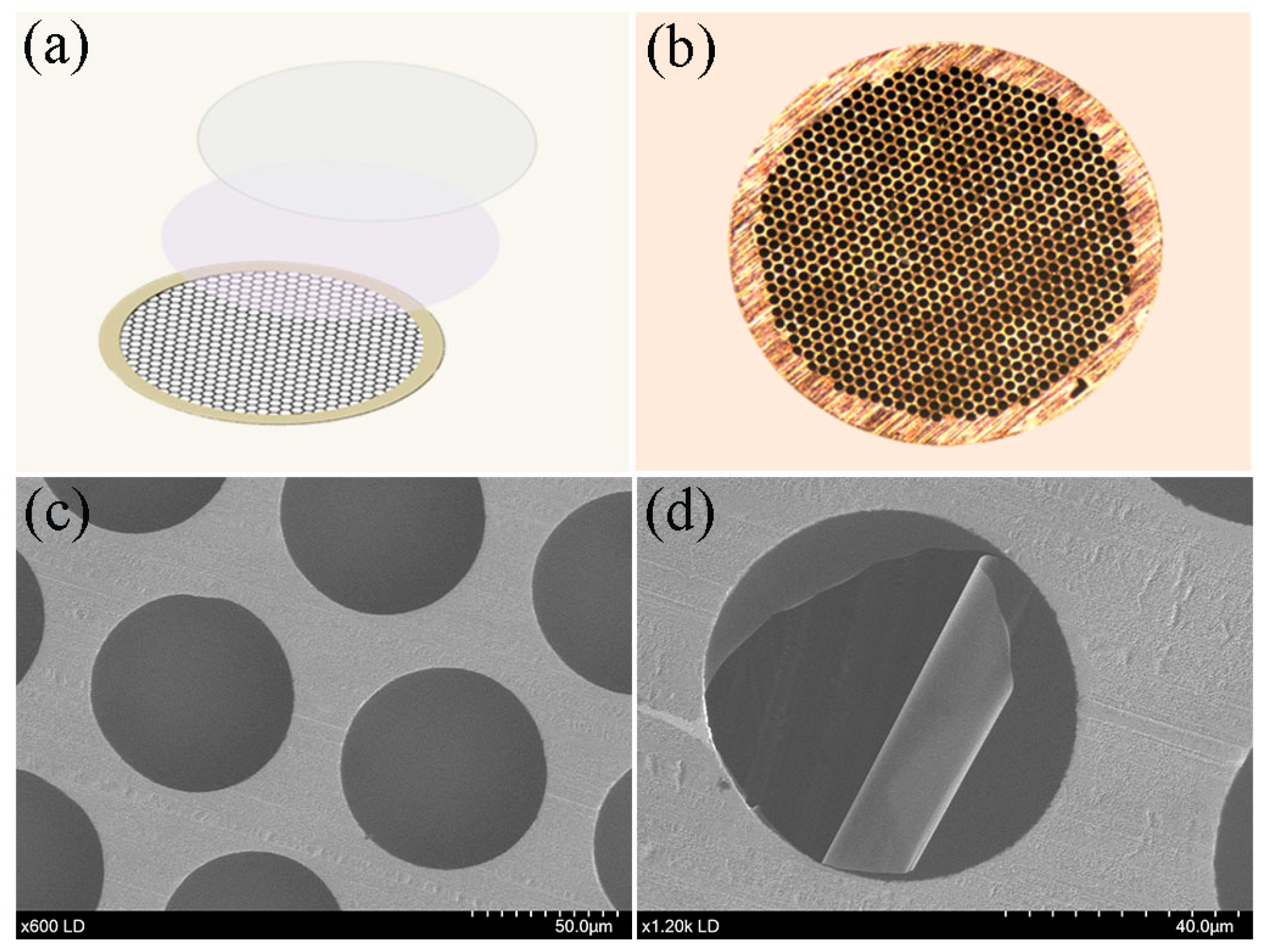
A conventional CSF, as shown in Figure 2a, typically consists of a bare copper grid with a diameter of about 3.05 mm, a polymer film (also known as Formvar film) and a carbon film. The carbon film is coated on the polymer film, and the latter is elastic, effectively preventing nanoparticles leakage through the grid holes. The carbon film is conductive to effectively prevent charge accumulation during EB irradiation. Figure 2b shows the optical image of a conventional CSF (230 mesh), and densely arranged holes are observed on the copper grid. The more detailed microstructure under SEM is displayed in Figure 2c, and the grid hole diameter is about 60 µm. The stacked carbon/polymer film can be clearly seen at the rupture site, as shown in Figure 2d.
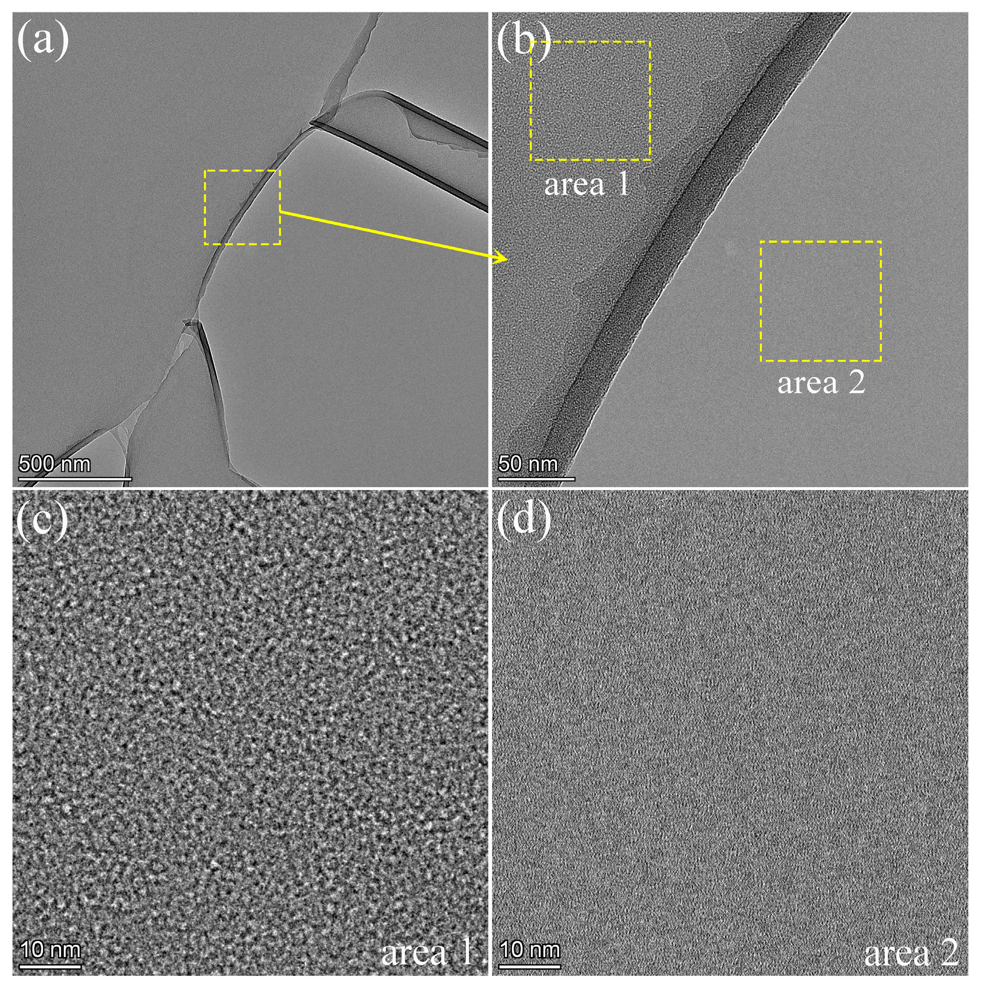
Conventional CSFs are suitable for visualizing the morphology contrast of nanoparticles. However, they are inadequate for HRTEM analysis of poorly crystalline nanomaterials or those exhibiting weak morphological contrast, which primarily arises from the pronounced background noise caused by the relatively thick carbon film (~15 nm). Figure 3a,b display the morphologies of a ruptured film. The HRTEMs of the carbon film region (area 1) and the film-free region (area 2) are respectively shown in Figure 3c,d, and it can be seen that the carbon film region exhibits uneven thickness and thus inconsistent contrast, while the film-free region displays uniform contrast. In TEM imaging, the contrast from the conventional CSF can interfere with the sample contrast. At higher magnification, this interference becomes more pronounced, ultimately degrading spatial resolution.

3.1.2. Conventional Holey CSFs

Just like conventional CSF, a conventional holey CSF also consists of a bare copper grid, a polymer film and a carbon film (Figure 4a). The key difference lies in the numerous micropores fabricated on the stacked polymer/carbon film. The detailed microstructures of the micropores are displayed in Figure 4b–d, and the micropore diameter distribution was broad, ranging from approximately 200 nm to 4 μm.
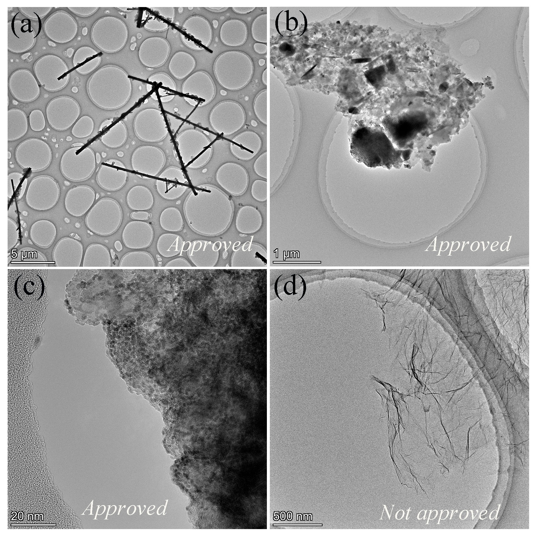
Conventional holey CSFs are suitable for 1D or 2D nanopowder with relatively large dimensions, such as short nanofibers, 2D gold flakes, nanocrystal clusters, and graphene. These materials can suspend across the micropores, which enables film-free observation and eliminates background interference, as shown in Figure 5a–c. Notably, 1D or 2D materials should possess sufficient mechanical strength to withstand the impact force exerted by high-density EB. Unsupported regions of less robust materials are prone to EB-induced drift, which severely degrades image quality. A representative example is shown in Figure 5d, where an ultrathin graphene is suspended over a microhole. Due to its low mechanical strength, such a structure is inherently prone to EB-induced drift, which would severely degrade image quality.

3.1.3. Ultrathin Holey CSFs

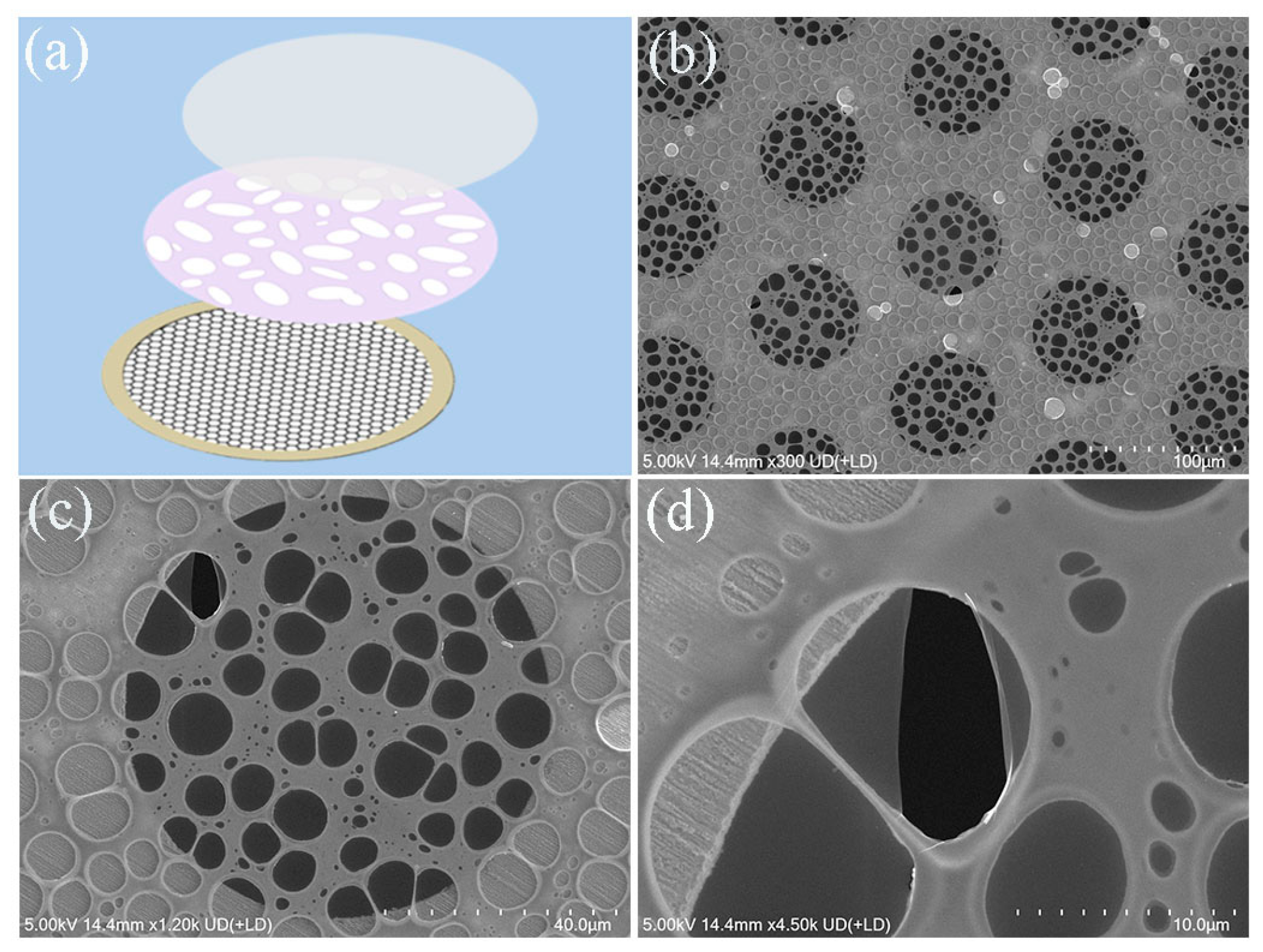
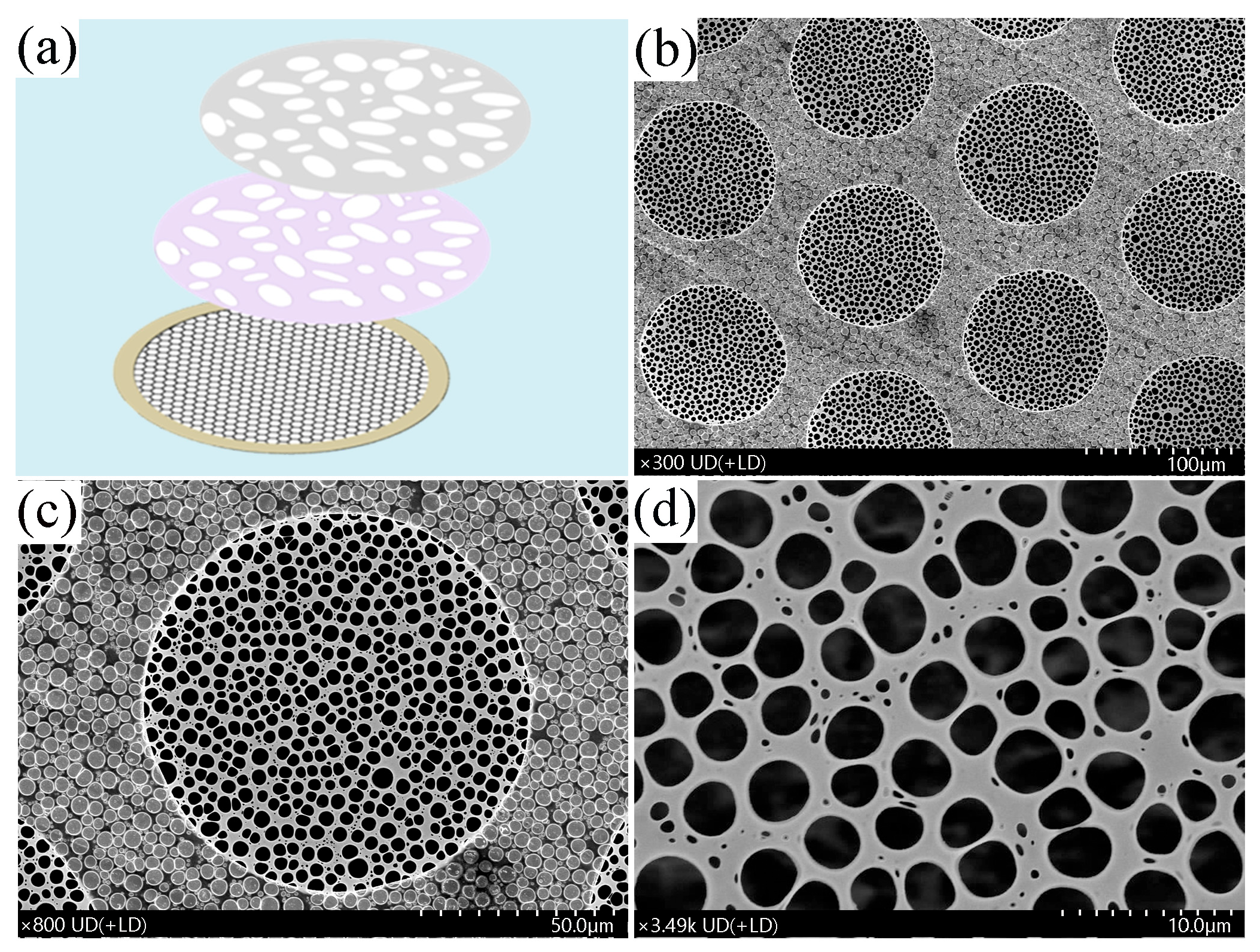
Figure 6a displays the diagrammatic sketch of an ultrathin holey CSF, and it consists of a bare copper grid, a micropore-rich polymer film, and an extremely thin (~5 nm), continuous carbon film without any micropores. The more detailed microstructures of the ultrathin holey CSF under SEM are displayed in Figure 6b–d, and the coated ultrathin carbon film can be clearly seen at the rupture site, as shown in Figure 6d.
Ultrathin holey CSF, characterized by its low background interference, is ideal for TEM observation of these low-contrast materials, such as sub-nanometer particles or ultrathin materials. Furthermore, the thin carbon film provides essential mechanical support to counteract the impact force exerted by EB, and its electrical conductivity effectively prevents charge accumulation, thereby minimizing image drift and ensuring high-resolution imaging. Kim et al. successfully used an ultrathin carbon film to characterize 26 nm rubber fume particles, which are representative low-contrast materials [19].

3.1.4. Double-Grid Support Films

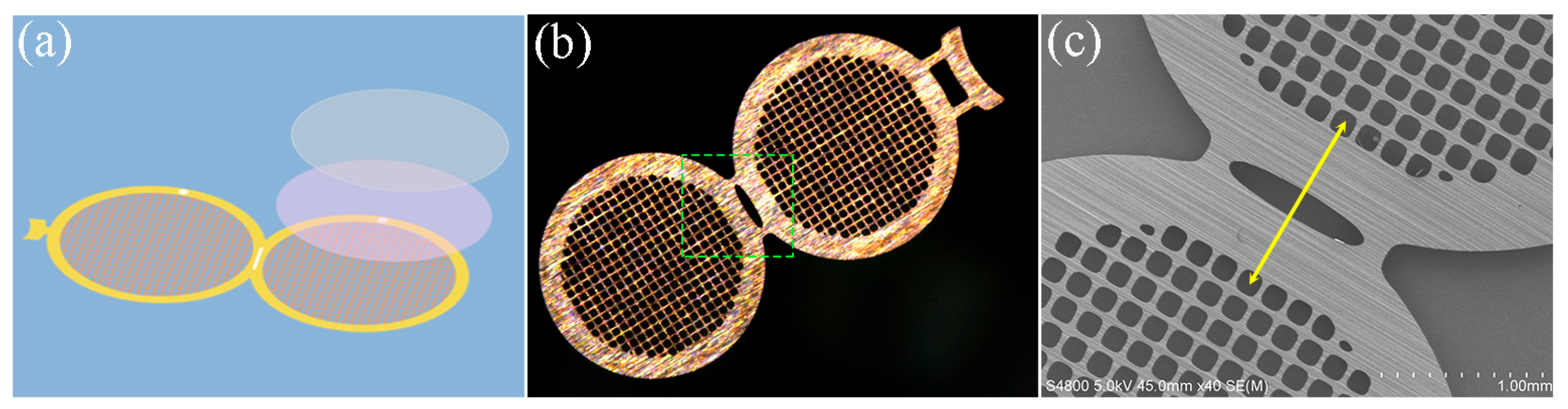
The diagrammatic sketch of a double-grid support film is displayed in Figure 7a. Depending on the application, this support film can be bare and can be coated with carbon/polymer film on either one grid or both grids. The optical morphology of a double-grid support film is shown in Figure 7b, and the more detailed morphology of the region delineated by the green square in Figure 7b is displayed in Figure 7c. In Figure 7c, it can be seen that the holes are distributed symmetrically on the paired grids, which can ensue the concentricity of the holes after the paired grids are folded together, maintaining the electron transparency in TEM imaging.
The double-grid support film provides mechanical entrapment and is particularly suitable for observing samples that adhere poorly to CSFs, such as electrospun fibers, nanowires, and large-area two-dimensional materials. A practical case using double-grid support films for sample preparation can be seen in Section 3.3.2. Furthermore, a double-grid support film coated with polymer/carbon film on both grids can mechanically clamp weakly magnetic nanoparticles, preventing their migration toward the pole pieces during TEM observation.
In summary, TEM CSFs are available in a diverse array of types with distinct morphological and functional properties. This diversity enables researchers to select an optimal CSF tailored to the specific requirements of different nanomaterials.

3.2. Critical Preparation Steps

In addition to an appropriate CSF, improper specimen preparation can still lead to sample aggregation, uneven distribution, or the introduction of contaminants, ultimately degrading imaging quality. In this section, we analyze the impact of key preparation steps on imaging quality by examining several samples.

3.2.1. Dispersion

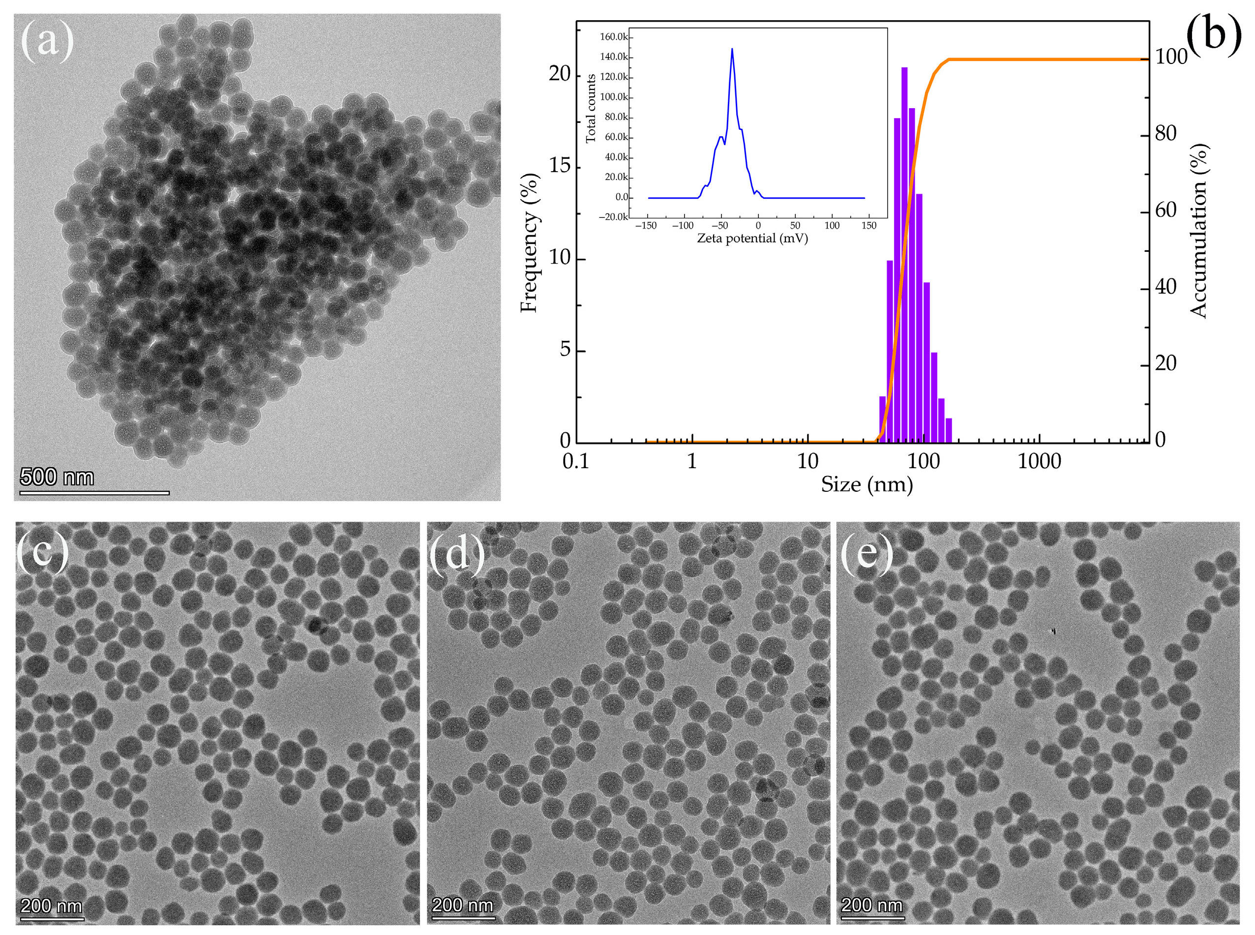
Nanoparticles are highly prone to agglomeration due to high surface energy. Figure 8a reveals the TEM morphology of the poorly dispersed SiO2 powder, it can be seen that the central region exhibits poor transparency owing to dense particle stacking, so the morphology contrast of the particles is blurred. To enhance dispersion quality, 6 mg of SiO2 powder was added to 10 mL of deionized water, followed by the addition of 5 mg of PEG. The mixture was then dispersed by ultrasonication for 15 min to obtain a suspension. Figure 8b shows the particle size distribution of the dispersed SiO2 nanoparticles, exhibiting a narrow peak with a median diameter of 68 nm, which suggests the effective elimination of particle agglomeration. The inset in Figure 8b displays the zeta potential distribution of the suspension, with a median potential of −35.6 mV (absolute value > 30 mV). This value suggests that the suspension possesses sufficient electrostatic stability [20]. Additionally, the PEG molecules adsorbed on the surface of the SiO2 nanoparticles provide steric hindrance. The combined effects of electrostatic repulsion and steric hindrance effectively inhibit particle agglomeration, ensuring a stable dispersion. The stable suspension was then drop-cast onto a conventional CSF for TEM observation, and the resulting images are shown in Figure 8c–e. It can be seen that the redispersed SiO2 nanoparticles displayed monodisperse morphology without detectable aggregation, allowing precise measurement of particle dimensions. Therefore, powder dispersion is a crucial step in the process of TEM sample preparation.
Nanoparticles vary significantly in morphology and surface characteristics, such as hydrophobicity, electrical properties, and adsorptivity, as well as in atomic-layer arrangement and functional groups. [21]. Therefore, appropriate dispersion methods, such as ultrasonic dispersion [22], mechanical dispersion [23], or surface modification techniques [24], should be tailored to different nanomaterials:
(1)
Carbon-based nanomaterials (e.g., carbon nanotubes, graphene): Carbon-based nanomaterials tend to easily form agglomerates due to their large specific surface area, van der Waals forces, and π-π conjugation interactions. Various dispersion methods have been developed for such nanomaterials. Kadhum et al. employed gum arabic to disperse carbon nanotubes through electrostatic interaction and then added the second dispersant (hydroxyethyl cellulose-10) to provide sufficient steric hindrance and maintain its dispersion stability [25]. The ball milling process, combined with chemical addition, suppresses the attraction between carbon nanotubes and effectively prevents their aggregation [26]. Xiong et al. used a sequential process involving edge oxidation, bubble expansion and mechanical shearing to disperse graphite flakes [27].
(2)
Metal oxide nanoparticles (e.g., TiO2, BaTiO3, Al2O3, MgO): Owing to their high specific surface area, these nanoparticles experience a sharp increase in surface-free energy, making them prone to agglomeration through van der Waals forces and chemical bonding. To overcome this issue, various dispersion strategies have been employed. The aggregated TiO2 dry powder (with a primary particle size of nearly 15 nm) was well dispersed by a mechanical milling method using small beads with a diameter of 15–30 μm [28]. Nanoparticle aggregates of BaTiO3, Al2O3, MgO, etc., were dispersed by surface modification techniques using surfactants [29,30,31].
(3)
Two-dimensional inorganic nanomaterials (e.g., MoS2, MXene): For MoS2, aqueous dispersion can be achieved by methods such as surfactant-assisted dispersion or surface energy modulation using ammonia solution [32]. BN nanosheets can be effectively dispersed via non-covalent surface modification with polyetherimide, where the adsorbed polymer chains create steric hindrance to prevent re-stacking [33].
Therefore, there is no universally effective method, and dispersion strategies must be tailored not only to the unique properties of different nanomaterials but also to the specific characteristics of each individual sample.

3.2.2. Organic Contaminant Treatment

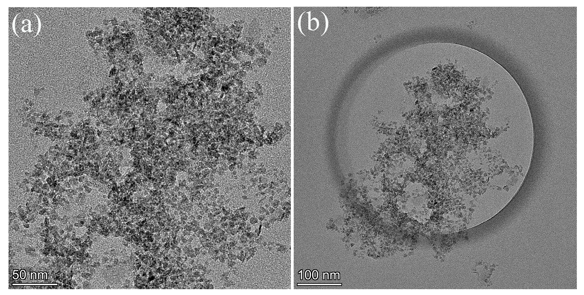
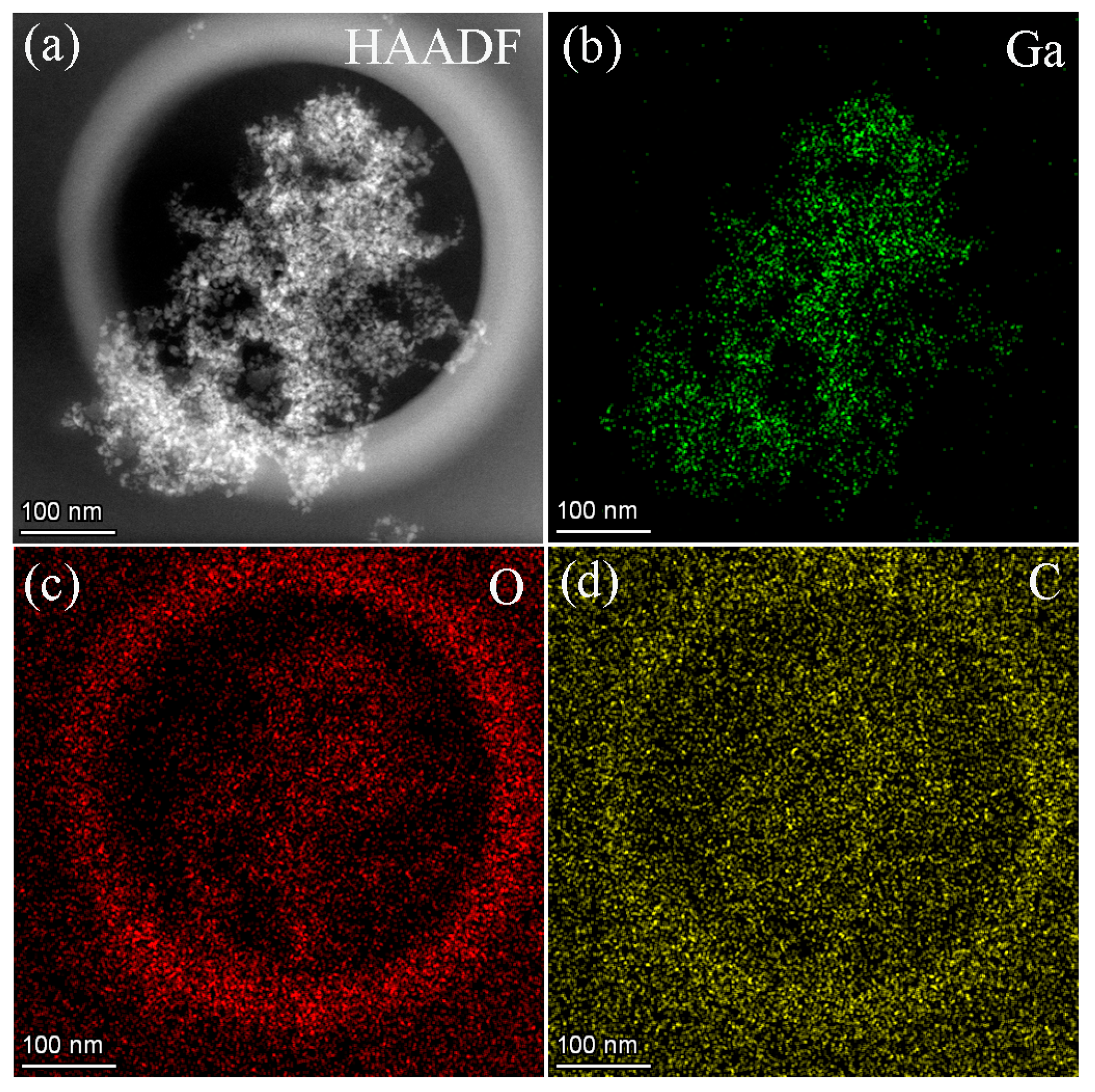
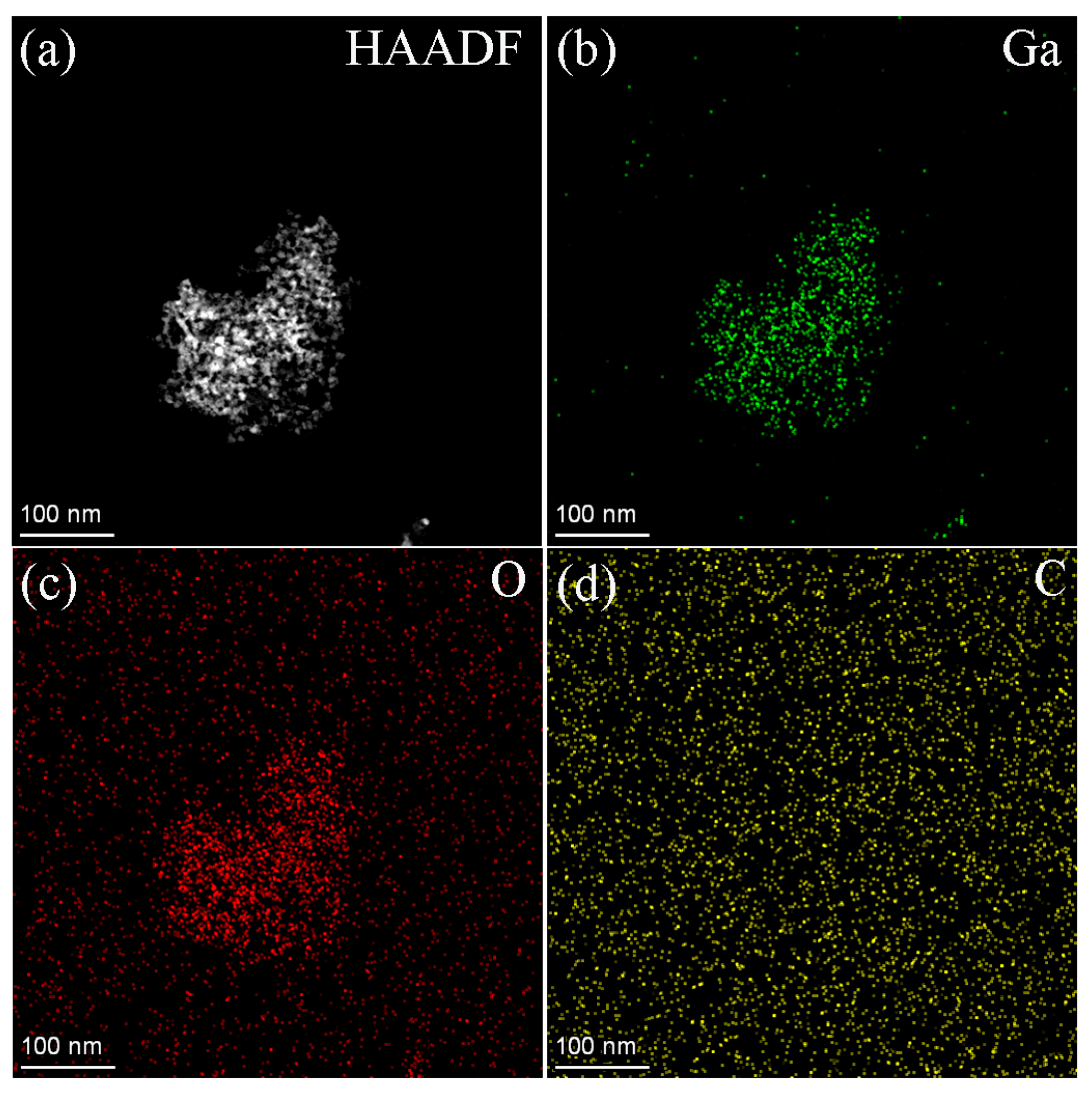
Organic residues can be introduced during the sample synthesis or the TEM sample preparation process. In TEM observations, organic contaminant is decomposed under EB irradiation, leading to the formation of positively charged carbon ions. These cations subsequently are trapped by the high-density electron cloud and deposit within or around the area irradiated by the EB. The deposited carbon ions can form a parasitic background, interfering with the true sample image. Figure 9a displays the morphology of Ga2O3 nanoparticles imaged at 190 kx magnification. When the magnification is lowered to 150 kx, the morphology is shown in Figure 9b; a black ring-shaped artifact is observed. EDS mapping was conducted on the region with the artifact to identify its chemical composition, which is shown in Figure 10. It can be seen that O (Figure 10c) and C (Figure 10d) are concentrated in the annular zone, which results from EB-induced decomposition of organic matter into OH radicals and carbon ions.
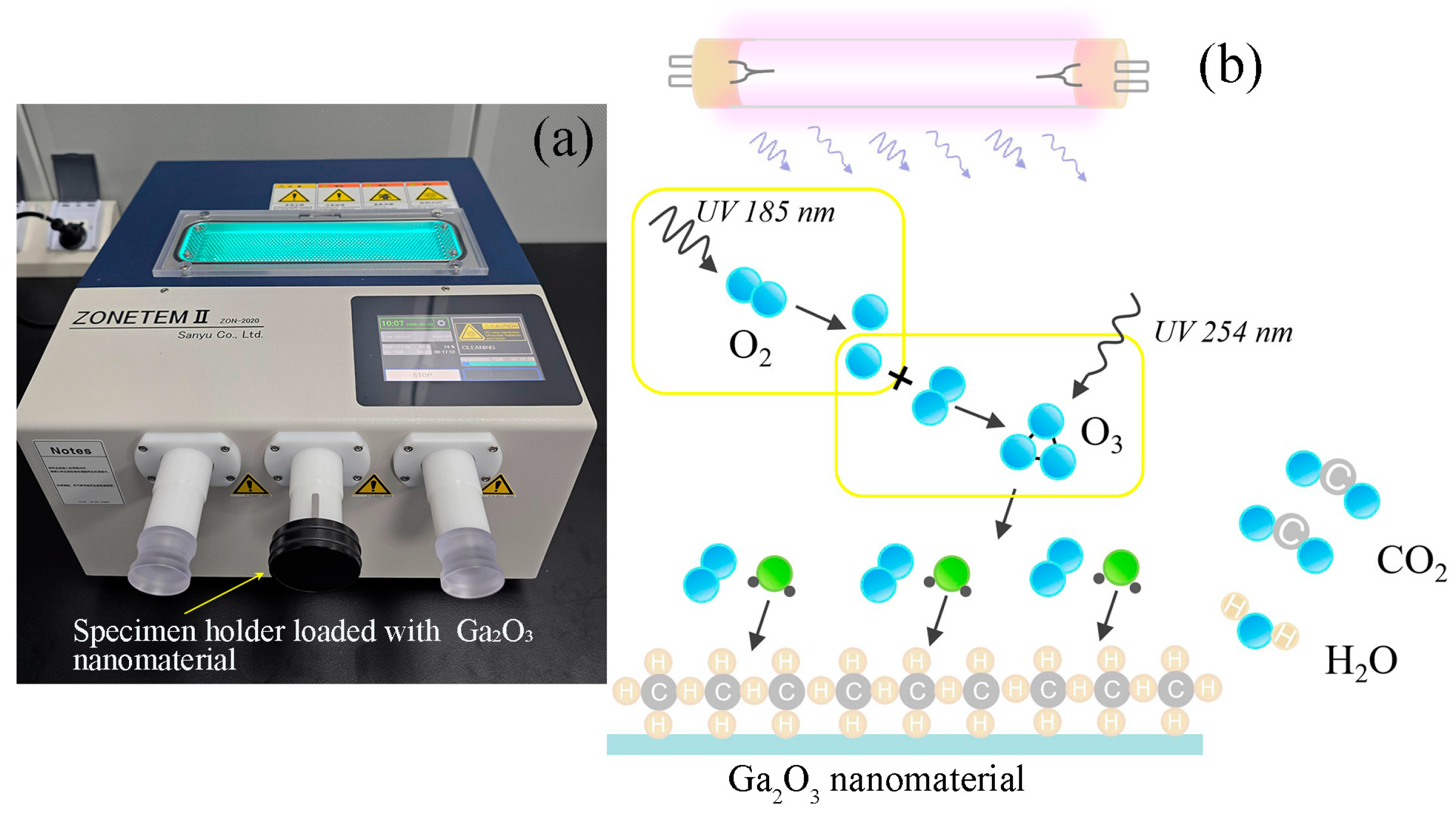
To effectively remove carbon contamination, the specimen holder loaded with the Ga2O3 nanomaterial was placed in a UV-ozone cleaner, as illustrated in Figure 11a. The cleaning process was carried out under the following conditions: 400 Torr chamber pressure and continuous 185/254 nm UV irradiation for 15 min. In the reaction chamber, as illustrated in Figure 10b, ozone (O3) is generated through 185 nm UV photodissociation of O2. Simultaneously, the 254 nm UV radiation photodissociates ozone, producing highly reactive oxygen atoms. These reactive oxygen atoms oxidize the C-C/C-H bonds of organic contaminant, converting them into H2O and CO2, which are subsequently removed by the gas flow system. Figure 12a displays the morphology of the retreated Ga2O3 nanomaterial at 190 kx. At the lower magnification of 150 kx, the morphology is shown in Figure 12b; no carbonaceous ring is observed. The EDS elemental maps shown in Figure 13 exhibit dominant Ga (Figure 13b) and O (Figure 13c) signals of Ga2O3. Meanwhile, the background signals of O (Figure 13c) and C (Figure 13d) from the CSF are weak and homogeneously distributed, indicating no carbonaceous deposition on the region. By using ozone cleaning prior to TEM observation, we successfully avoided the formation of carbon deposition.

3.3. Several Case Studies in TEM Sample Preparation for Nanopowder of Different Dimensions

3.3.1. Zero-Dimensional Nanopowder (A Case Study on ZnO Nanocrystals)

Zero-dimensional nanopowders, such as quantum dots [34], nanocrystals [35], and oxide nanoparticles [36], etc., are prone to severe aggregation due to their ultra-small sizes (typically a few nanometers). A critical challenge in TEM sample preparation for 0D nanomaterials lies in achieving effective dispersion to prevent nanoparticle stacking on CSFs. Subsequently, the influence of the dispersion efficacy of 0D nanopowder on the imaging quality is investigated, using ZnO nanocrystals (~1 nm) as a representative case.
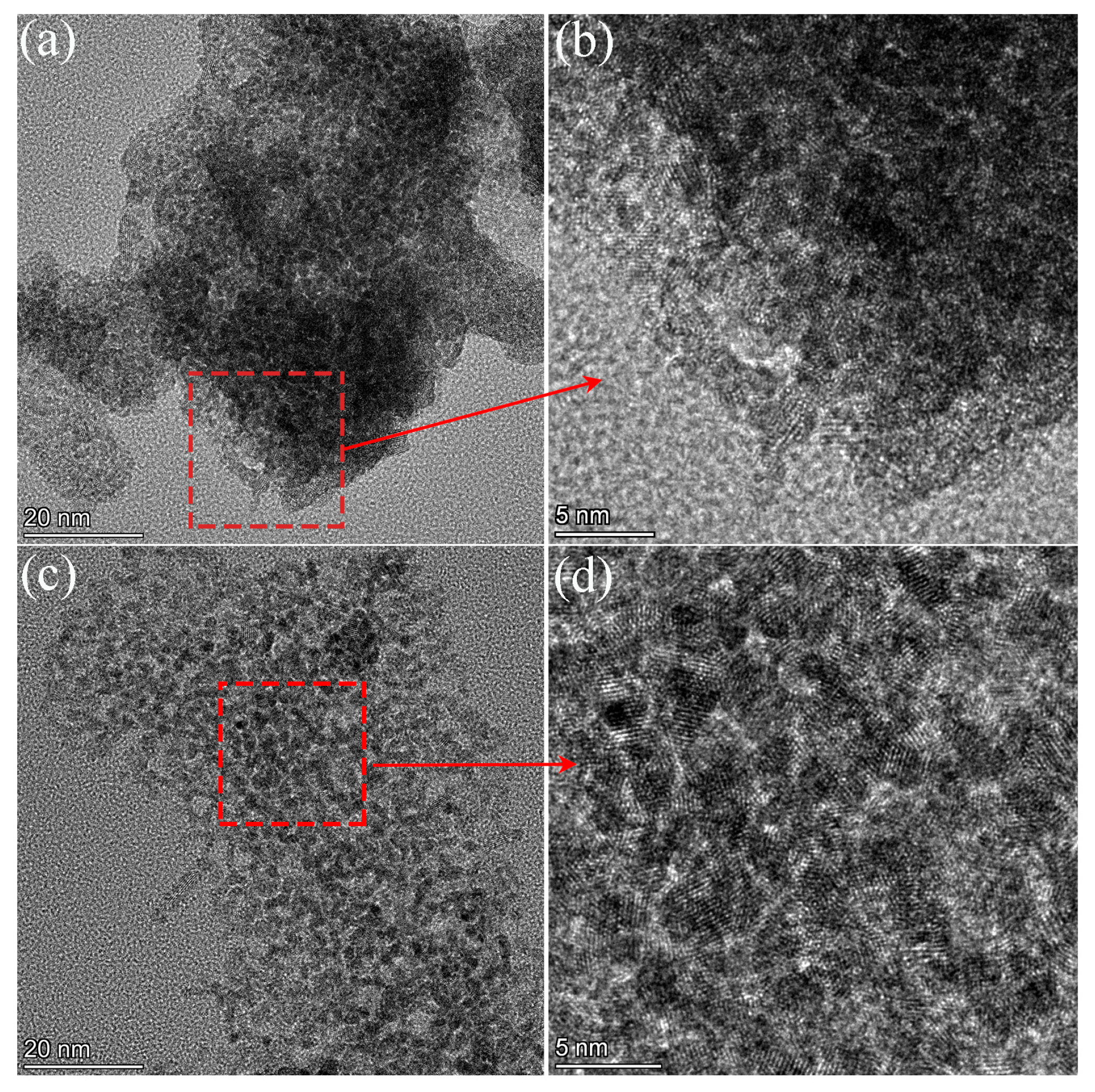
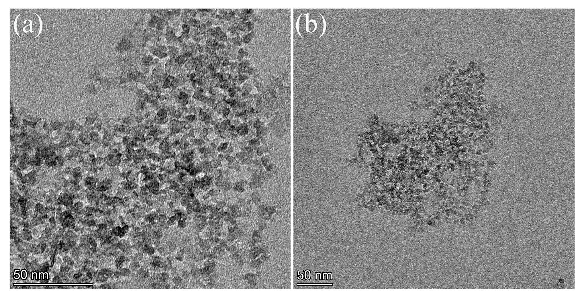
When following the conventional sample preparation procedure proposed in “materials and methods” section, after 15 min of ultrasonication, the ZnO nanoparticle suspension was dropped onto a conventional CSF for TEM analysis. The resulting morphology, characterized by severe particle agglomeration, is shown in Figure 14a. This agglomeration led to poor transparency and weak particle contrast in TEM imaging. The magnified morphology of the region delineated by the red square in Figure 14a is shown in Figure 14b; the crystal lattices of the nanoparticles at the nanocluster edge can be clearly observed, while those in the thicker interior regions remain unresolved.
To enhance dispersion quality, the TEM sample preparation protocol for ZnO nanoparticles was optimized as follows: 6 mg PVP K30 was added to 10 mL of ethanol containing 3 mg ZnO nanoparticles. After 15 min of ultrasonication, the suspension was dropped onto a conventional CSF. As shown in Figure 14c, the resulting morphology demonstrates well-dispersed nanoparticles with clear contrast and minimal particle stacking. The HRTEM image of a randomly selected region (delineated by the red square) in Figure 14c is displayed in Figure 14d.
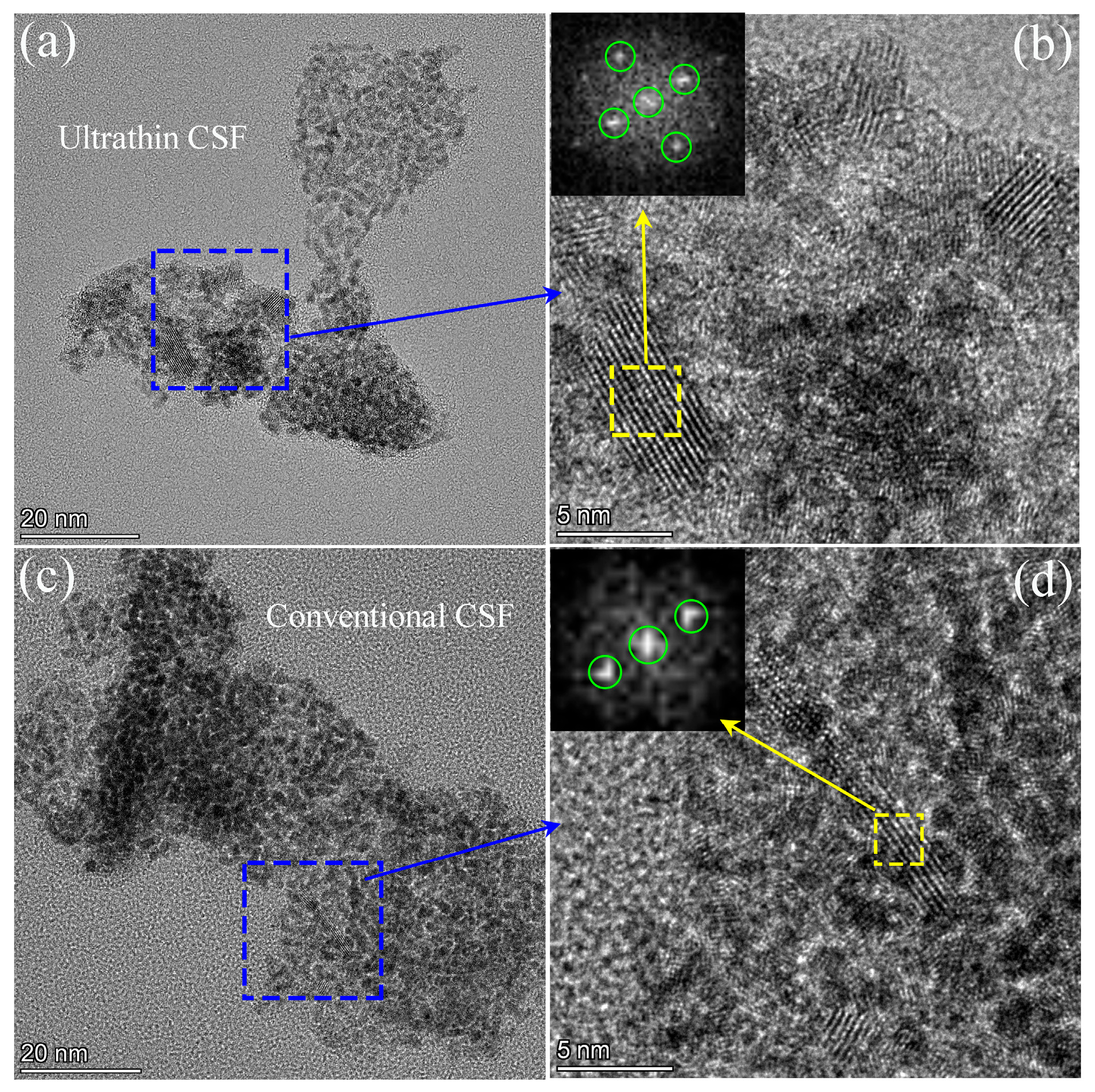
From Figure 14d, the crystal lattices of all nanocrystals within the area can be clearly resolved. Thus, the optimization of the dispersion method effectively suppressed particle stacking, contributing to a substantial improvement in both morphology and phase contrast. However, it can be seen from Figure 14b,d that the background noises from conventional CSF are pronounced. For better imaging quality with negligible background interference, the ultrathin holey CSF was employed as the support film of ZnO particles. Following the optimized sample preparation protocol mentioned above, ZnO suspension was sequentially dropped onto an ultrathin holey CSF and a conventional CSF for comparative analysis.
The micrograph and the HRTEM displayed in Figure 15a,b are for ZnO nanoparticles on the ultrathin holey CSF; those displayed in Figure 15c,d are for those on the conventional CSF. Figure 15a,b display a smoother background than in Figure 15c,d. The sizes and the lattice spacings of ZnO nanoparticles were statistically analyzed using the scale tool in the Velox software (version 3.8) of the Thermo Scientific Talos F200S system. The average particle size of the ZnO nanoparticles on the ultrathin holey CSF is approximately 1.27 nm. The average lattice spacing of ZnO nanoparticles on conventional CSF is 0.3153 nm; on ultrathin holey CSF, it is 0.3243 nm, which is in good agreement with the theoretical lattice constant of 0.325 nm reported for wurtzite ZnO [37]. Furthermore, the ZnO nanocrystals in Figure 15b exhibit more numerous lattice fringes than those in Figure 15d. As shown by a comparison of the insets in Figure 15b,d (FFT diffractograms from the yellow square-delineated regions), the increased number of lattice fringes generates additional Bragg diffraction spots at distinct angular positions, enabling more accurate unit cell parameters [38].

3.3.2. One-Dimensional Nanomaterials

One-dimensional nanomaterials encompass nanorods [39] (sub-100 nm in length), nanowires (1–50 μm in length), electrospun fibers (mm-scale and beyond in length) [40], etc. Appropriate CSFs can be selected according to the longitudinal dimension.
Table 1 summarizes the recommended CSFs for 1D nanomaterials. For nanorods, if their length L is smaller than d (d is the micropore diameter of the conventional holey CSF, as shown in the insert in Table 1), sample leakage through the micropores is possible. Therefore, conventional CSFs are recommended to avoid this issue. When the length L of nanorod or nanofiber exceeds d but remains below D (D is the grid hole diameter, as shown in the insert in Table 1), conventional holey CSFs become preferable, as they help minimize background interference. For significantly long nanofibers (e.g., electrospun fibers with length LD), double-grid support films are recommended, as such lengthy nanomaterials tend to detach or drift on conventional CSFs due to inadequate adhesion.
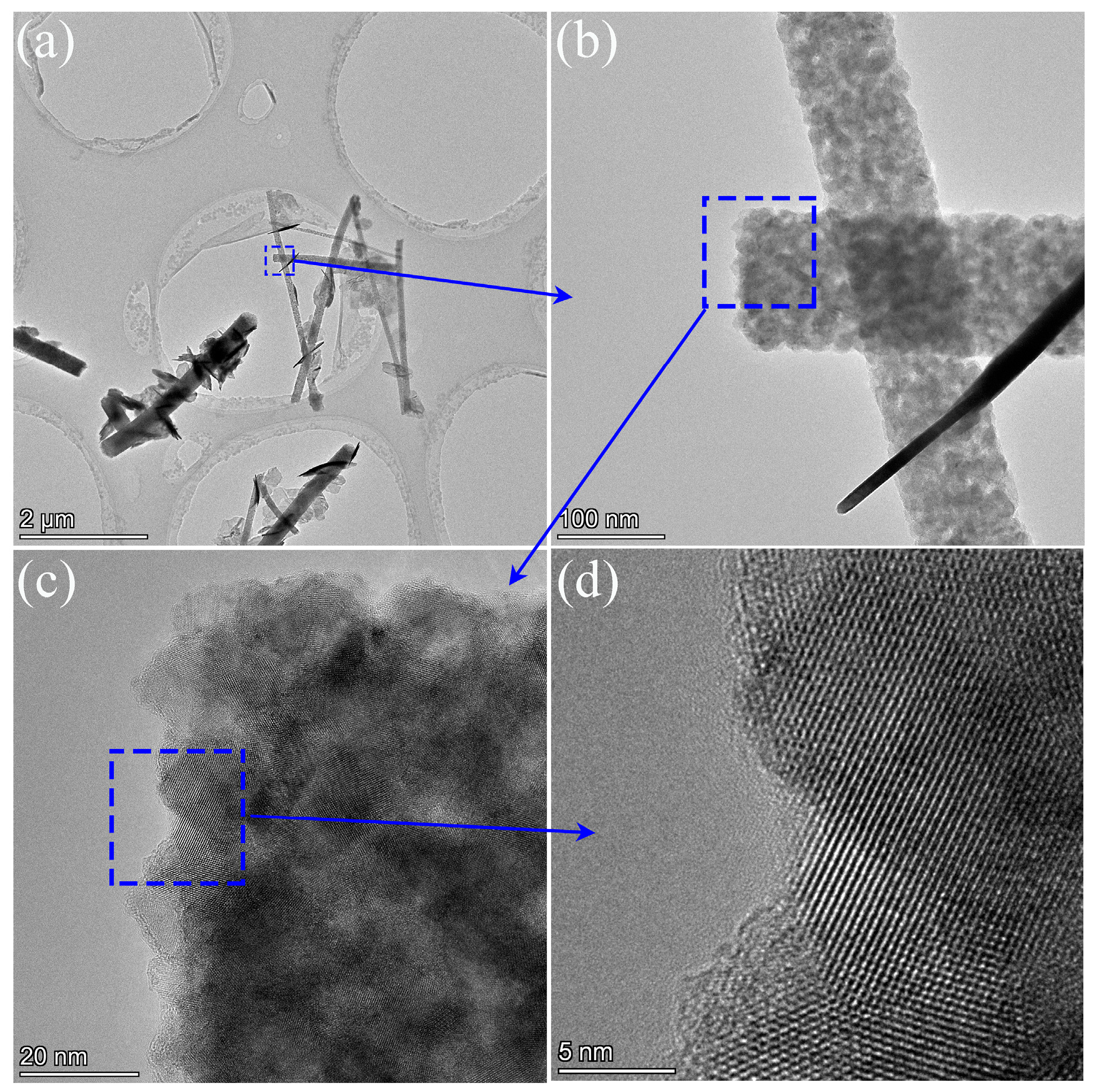
Figure 16 shows the TEM morphologies of short TiO2 nanofibers (~10 µm in length) prepared on a conventional holey CSF. It can be seen from Figure 16a, the nanofibers suspend across the micropores. Higher-magnification images are displayed in Figure 16b,c, which both display good morphological contrasts. The HRTEM image presented in Figure 16d exhibits well-resolved lattice fringes with no visible background interference.
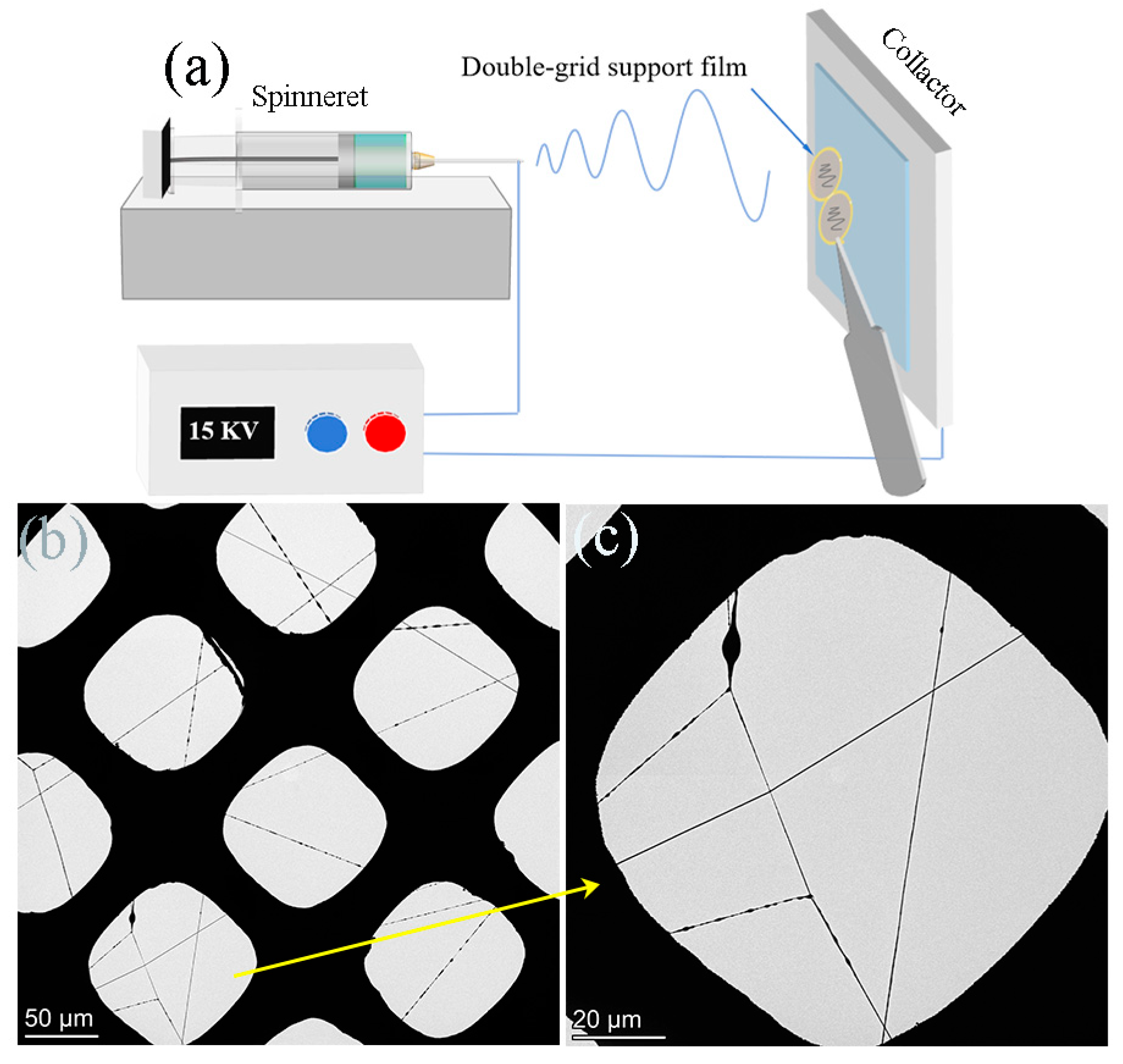
Ultra-long fibers fabricated by electrospinning cannot be effectively deposited onto conventional CSF. Taking polyurethane-dextran fibers as a case study, following the procedure shown in Figure 17, with its support side facing the spinneret, a double-grid support film with carbon film on both grids was positioned near the flat plate collector. During electrospinning, the charged jet was stretched and attenuated under a high-voltage electrostatic field, generating ultrafine polyurethane-dextran fibers that were randomly deposited onto the surface of the support film, achieving in situ fiber attachment. After collecting for ~20 s to reach a suitable fiber density, the double-grid support film was air-dried at room temperature, folded for fixation, and then subjected to TEM observation. The resulting micrographs (Figure 17b,c) confirm that the electrospun fibers were successfully clamped between the folded grids, demonstrating the suitability of this in situ collection method for the preparation of long fibers. Such a double-grid support film with carbon film is essential for organic polyurethane-dextran fibers with low mechanical robustness, as they are susceptible to displacement or rapid structural collapse under high-density EB irradiation.
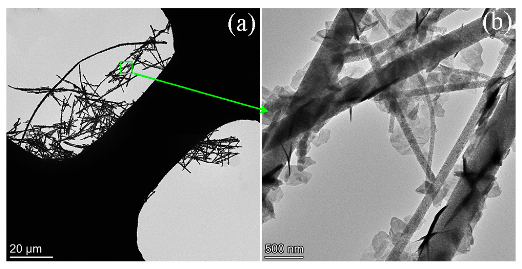
In addition to freshly prepared electrospun fibers collected in situ for TEM observation, electrospun fibers that had undergone post-treatment (e.g., calcination or carbonization) were also investigated. Here, electrospun TiO2 nanofibers, which were further decorated with BiOCl nanosheets through a subsequent solvothermal process, are used as an example. The sample preparation method and corresponding TEM observation results are illustrated as follows. The fabric was first cut into fragments smaller than 2 mm and dispersed in anhydrous ethanol. A bare double-grid support film was then used to scoop the fibers from the suspension, allowing them to attach onto the grid surface. After folding and air drying at room temperature, the grid was gently blown with a nitrogen gun or rubber bulb to remove any loosely attached fibers. The resulting TEM morphologies are displayed in Figure 18. Figure 18a shows a cluster of fibers clamped between two grids. Figure 18b reveals outstanding morphology contrast with negligible background noise. It is noteworthy that the TiO2 nanofibers made of inorganic materials possess sufficient mechanical strength to withstand the impact of high-energy EB, preventing specimen drift during focusing, thus allowing the use of bare double-grid support films. However, organic electrospun fibers with low mechanical robustness are prone to displacement or rapid structural collapse under high density EB, so double-grid support films with carbon/polymer film are mandatory for these fibers.

3.3.3. Two-Dimensional Nanomaterials (A Case Study on Ti3C2 MXene)

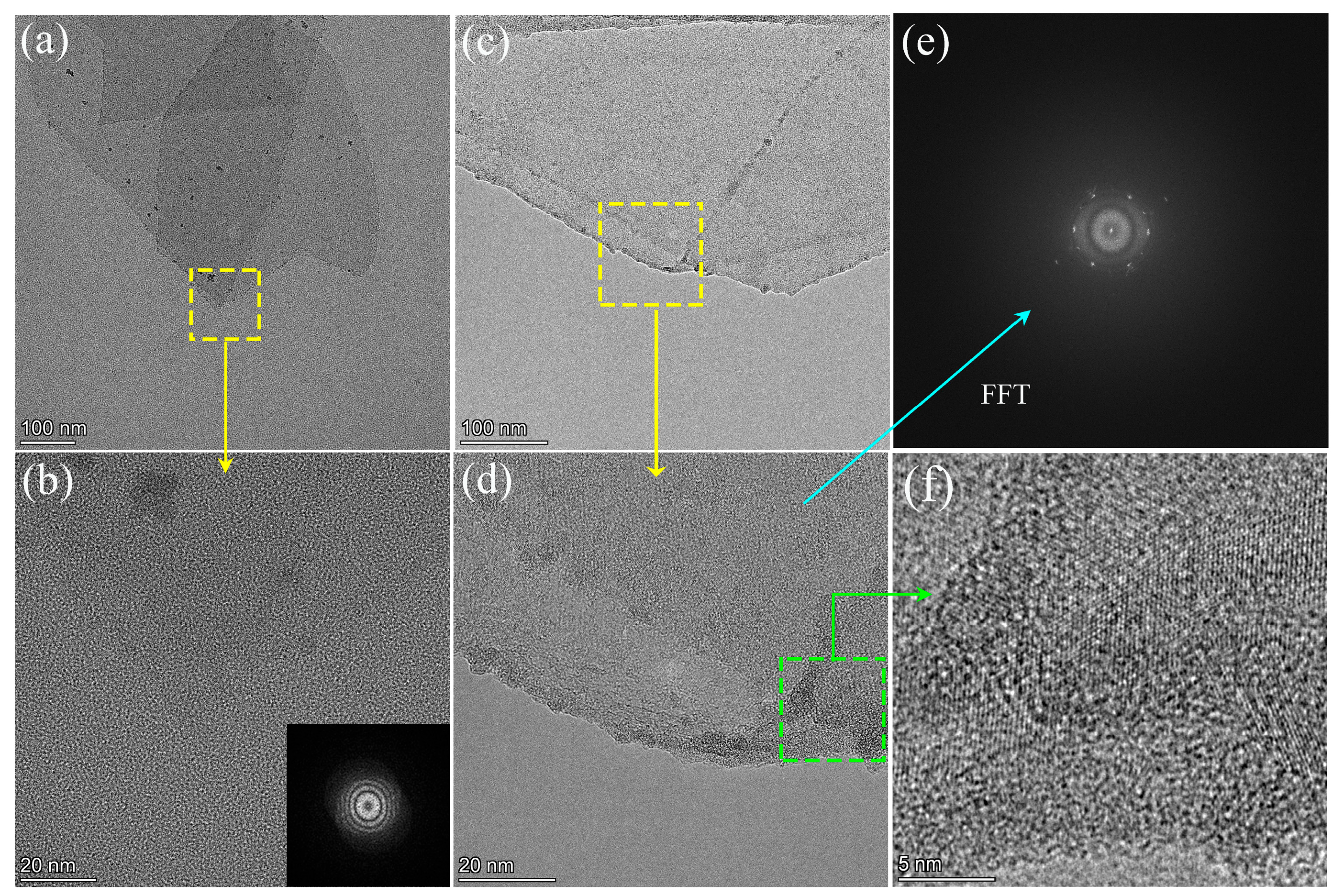
Two-dimensional nanomaterials such as MXene and grapheme, which are atomic-scale in thickness, exhibit weak electron scattering, resulting in very weak contrast on conventional CSFs. Figure 19a,b show the TEM images of Ti3C2 MXene on a conventional CSF. It can be seen from Figure 18a that the morphology contrast is clear at low magnification. However, when the region delineated by the yellow square in Figure 19a is imaged at higher magnification (300 kx), the contrast is markedly reduced, as seen in Figure 19b. The corresponding FFT in the inset of Figure 19b exhibits only diffuse halos originating from the amorphous carbon film.
To obtain clear contrast, we initially used a conventional holey CSF containing film-free micropores, with the MXene nanosheets suspended over the micropores, allowing background-free observation. However, at high magnification, image drift occurred. This is attributed to the poor mechanical support of the ultrathin MXene nanosheets, which are easily displaced under the force exerted by high-density EB. Therefore, we employed an ultrathin holey CSF for imaging. It can be seen from Figure 19c that the morphology contrast is exceptionally sharp at low magnification. At higher magnification of 300 kx (Figure 19d), the contrast remains clear with negligible background noise. Furthermore, the diffraction spots (in Figure 19e) obtained via FFT from Figure 19d also appeared, and the lattice fringes (in Figure 19f) of the region denoted by the green square are also visible, which indicates that the ultrathin holey CSF effectively suppresses background noise, thereby allowing the phase contrast of Ti3C2 MXene to be clearly revealed. This phenomenon can be theoretically explained by the weak-phase object approximation (WPOA) [41], the exit wave function q(x,y). A sufficiently thin specimen is approximately related to the projected potential as follows:
q x , y 1 + i σ V t ( x , y ) ,
where σ = π / λ U , t is the specimen thickness and the Vt (x, y) is projected potential of the thin specimen. The diffracted wave Q(u, v) is generated via Fourier transformation of the exit wave at the back focal plane of the objective lens.
Q u , v = F q ( x , y ) ,
where (u, v) are the reciprocal coordinates at the back focal plane, and Q(u, v) can be simplified to Q(u) in the case of azimuthal symmetry along the optical axis. Considering the phase modulation by the spherical aberration Cs and the amount of defocus Δ f ,
Q u = Q ( u ) e i χ ( u ) ,
where χ u = π ( Δ f λ u 2 + 0.5 C s λ 3 u 4 ) .
Using the theorem of convolution operation, the wave function on an image plane can be expressed as
ψ x , y = 1 σ V t x , y F 1 s i n χ u + i σ V t x , y F 1 c o s χ u .
The intensity distribution in the image plane is therefore given by
I x , y = ψ x , y 2 = 1 2 σ V t x , y F 1 s i n χ ( u ) .
The Ti3C2 MXene is dispersed on the CSF. Based on the linearity of the WPOA, the total projected potential is the sum of those of the Ti3C2 MXene and the CSF. Therefore, the image intensity can be expressed as
I t o t a l x , y = 1 2 σ V t M ( x , y ) + V t C ( x , y ) F 1 s i n χ ( u ) ,
where V t M ( x , y ) and   V t C ( x , y ) are, respectively, the projected potential of MXene and the CSF; s i n χ ( u ) is the phase contrast transfer function (PCTF).
Let ϕ t M = σ V t M (x,y) and ϕ t C = V t C ( x , y ) ,
I t o t a l x , y = 1 2 ϕ t M + ϕ t C F 1 s i n χ ( u )
where ϕ t M and   ϕ t C are, respectively, the phase shifts in MXene and the CSF.
From Equation (7), it can be seen that during image formation, both the phase shifts of the MXene and the CSF are simultaneously convoluted with PCTF. Therefore, the phase shift from the CSF inevitably interferes with the MXene signal during imaging. First, the phase shifts induced by conventional and ultrathin CSFs are calculated, respectively. For conventional CSF,
ϕ t C = σ V t C = σ V 0 t C
for an acceleration voltage of U = 200 KV (corresponding to an electron wavelength of λ = 0.00251 nm), σ = 0.00625 V−1nm−1. For carbon-based materials, the mean inner potential V0 is typically taken as 15 V [42]. t is the thickness that the transmitted electrons pass through. For a conventional CSF, t is approximately 15 nm. Inserting these values into Equation (8), we get ϕ t C = 1.4   r a d .
For an ultrathin CSF with a thickness of t = 5 nm, the phase shift is reduced to ϕ t C = 0.47 rad accordingly.
The phase shift caused by the conventional CSF (1.4 rad) is much larger than that of the ultrathin CSF (0.47 rad). Therefore, a larger phase shift results in stronger interference with the MXene signal, which explains why MXene lattice fringes are difficult to observe on conventional CSF but can be clearly resolved on ultrathin CSF.

3.3.4. Practical Limitations

Despite the successful demonstration of the protocols described above, certain limitations remain that may affect their applicability to specific sample types or experimental setups.
(1)
UV-ozone cleaning: This cleaning technique is effective for thin surface contaminants but does not remove bulk organic material trapped inside dense agglomerates, because UV radiation cannot penetrate into the interior of thick contaminant layers or dense agglomerates. Therefore, in practice, to maximize the cleaning efficiency, it is necessary to fully disperse the agglomerates and ensure that the sample is deposited as a thin layer on the carbon film prior to UV-ozone treatment. Furthermore, although UV-ozone cleaning is relatively milder than plasma cleaning, prolonged exposure during contaminant removal may pose a risk of damage to materials such as graphene and organic samples.
(2)
Ultrathin holey CSFs (<5 nm): These CSFs are generally considered fragile and may be susceptible to damage under certain conditions, such as prolonged high-dose electron irradiation. Therefore, caution is still required when using ultrathin holey CSFs. Specifically, they should only be used to support well-dispersed small nanoparticles or thin two-dimensional materials. Furthermore, careful operation is necessary during sample preparation to avoid mechanical damage.
(3)
Double-grid support films: In practice, for stiff or thick fibers, folding is not only difficult but also can also easily destroy the fragile support film. For such samples, alternative preparation methods such as ultramicrotomy or focused ion beam (FIB) should be used.
(4)
PEG/PVP dispersants: the PEG/PVP dispersants are not suitable for hydrophobic, charged, or very high-aspect-ratio nanoparticles without further optimization. In this work, PEG was used specifically for SiO2 nanoparticles in Section 3.2.1, and PVP for ZnO nanoparticles in Section 3.3.1.

4. Conclusions

This work focuses on TEM specimen preparation for non-magnetic nanopowders. The structural characteristics and application suitability of several commonly used CSFs were investigated. The impact of key preparation steps, including dispersion and organic contaminant removal, on imaging quality was analyzed. Case studies encompassing nanomaterials of different dimensionalities were carried out.
(1)
The structural and morphological characteristics of the CSFs were characterized, and their applicability to different sample types was assessed. Conventional CSFs are suitable for morphological observation of nanoparticles. However, high-resolution imaging of low-contrast specimens is difficult to achieve due to the pronounced background noise generated by their relatively thick carbon film. Conventional holey CSFs are suitable for 1D or 2D nanomaterials whose largest dimension falls between their micropore and grid hole diameters, enabling background-free imaging. Ultrathin holey CSFs, characterized by extremely low background interference, are ideal for high-resolution observation of sub-nanometer particles or ultrathin 2D materials. Double-grid support films are suitable for samples with poor surface adhesion on conventional grids, such as electrospun fibers, nanowires, and large-area 2D nanomaterials.
(2)
Specific case studies illustrate that key preparation steps, including dispersion and organic contaminant removal, significantly affect subsequent imaging quality. Agglomerated SiO2 nanoparticles were well dispersed with the addition of dispersant and ultrasonication, as evidenced by a narrowed particle size distribution and TEM morphology of monodisperse particles. Ga2O3 nanoparticles encapsulated by organic contaminants were effectively cleaned by UV-ozone treatment, yielding clear TEM images and no observable carbon deposition under electron beam irradiation.
(3)
Through case studies on nanomaterials of different dimensions, the critical influence of preparation procedures or carbon film selection on imaging quality was demonstrated. For 0D ZnO nanocrystals, severe agglomeration was observed using the conventional preparation protocol, which was effectively suppressed by adding PVP followed by dispersion. Furthermore, replacing the conventional CSF with an ultrathin holey CSF yielded a smoother background and more observable lattice fringes, thereby generating additional Bragg diffraction spots and enabling more accurate unit cell parameter determination. For 1D nanomaterials, recommendations for CSF selection were provided based on their length differences, as demonstrated in specific examples. Compared with conventional CSFs, ultrathin holey CSFs enable clear resolution of lattice fringes of ultrathin 2D Ti3C2 MXene at high magnification. Theoretical calculations further demonstrated that the phase shift induced by ultrathin holey CSFs is only 0.47 rad, lower than the 1.4 rad induced by conventional CSF, indicating that the ultrathin holey CSF causes significantly less interference with the high-resolution imaging signal of the Ti3C2 MXene. This finding is consistent with the experimental results.
Additionally, the proposed protocols are effective but have specific limitations. UV-ozone cleaning cannot remove buried contaminants and may damage sensitive materials. Ultrathin holey CSFs are fragile and require careful handling. Double-grid support films are unsuitable for stiff or thick fibers. These limitations should be considered when applying the methods to different samples.

Author Contributions

J.S.: conceptualization, methodology, writing—original draft., Z.W., D.L., S.F. and Q.Y.: data curation, H.X.: resources, L.L.: writing—review and editing, resources. All authors have read and agreed to the published version of the manuscript.

Funding

This work was supported by the scientific research start-up fund of Anhui polytechnic university (No. 2022YQQ054 and 2023YQQ020), Anhui province key laboratory of intelligent car wire-controlled chassis system (No. QCKJJ202507), the interdisciplinary program of Wuhan National High Magnetic Field Center (No. WHMFC2025024), the foundation of Zhejiang key laboratory of multiomics and molecular enzymology (No. 2025YB005) and fund project of Anhui provincial engineering research center for vehicle display integrated system (No. VDIS&TDMD2024D01).

Institutional Review Board Statement

Not applicable.

Informed Consent Statement

Not applicable.

Data Availability Statement

The original contributions presented in this study are included in the article. Further inquiries can be directed to the corresponding author.

Conflicts of Interest

The authors declare no conflicts of interest.

Abbreviations

The following abbreviations are used in this manuscript:
TEMTransmission electron microscopy
EBElectron beam
PEGpolyethylene glycol
PVPpolyvinylpyrrolidone
CSFcarbon support films
HRTEMHigh-resolution transmission electron microscopy

References

  1. Williams, D.; Carter, C. The transmission electron microscope. In Transmission Electron Microscopy, a Textbook for Materials Science, 2nd ed.; Plenum Press: New York, NY, USA; London, UK, 2009; Volume 1, pp. 3–22. [Google Scholar]
  2. Wang, Y.; Gui, H.; Li, X.; Dong, Y.; Yang, X.; He, Z.; Zhao, D.; Yang, Y.; Zhao, H. Exploring the effect of grain/phase boundary transition phases on the wear resistance of Ni-based metal-ceramic composite coatings: Based on experimental study and finite element analysis. Tribol. Int. 2025, 211, 110846. [Google Scholar] [CrossRef]
  3. Bustos, L.; Vasile, F.; Ruiz-Henestrosa, V.; Carrera-Sánchez, C.; Pérez, O. Buffalo whey proteins-vitamin E macromolecular bioinspirated complexes. Formation and performance at air/water interface. Colloids Surf. A 2025, 718, 136871. [Google Scholar] [CrossRef]
  4. Zhang, W.; Li, L.; Shu, Y.; Wang, J. Coordination catalysis of metals and polydopamine enables controlled release of CO from MnCO by enhancing oxidative stress and the thermal effect. Inorg. Chem. Front. 2024, 11, 5196–5209. [Google Scholar] [CrossRef]
  5. Zhong, X.; Liang, G.; Meng, L.; Xi, W.; Gu, L.; Tian, N.; Zhai, Y.; He, Y.; Huang, Y.; Jin, F.; et al. Automated Particle Size Analysis of Supported Nanoparticle TEM Images Using a Pre-Trained SAM Model. Nanomaterials 2025, 15, 1886. [Google Scholar] [CrossRef]
  6. Tokunaga, T.; Saito, K.; Kuno, K.; Higuchi, K.; Yamamoto, Y.; Yamamoto, T. Removal of carbon contamination in ETEM by introducing Ar during electron beam irradiation. J. Microsc. 2019, 270, 46–52. [Google Scholar] [CrossRef]
  7. Hayashida, M.; Yamasaki, J.; Malac, M. Sample thickness affects contrast and measured shape in TEM images and in electron tomograms. Micron 2024, 177, 103562. [Google Scholar] [PubMed]
  8. Yuan, F.; Tu, C.; Yu, J.; Cui, Z. High-pressure dispersion of nanoparticle agglomerates through a continuous aerosol disperser. Appl. Nanosci. 2019, 9, 1857–1868. [Google Scholar] [CrossRef]
  9. Armbruster, B.; Anzalone, P.; Kosmowska, E.; Lopez, E.; Novak, A. The effects of plasma cleaning on carbon and hydrocarbon-contaminated samples and quantification of decontamination in the scanning electron microscope. Microsc. Microanal. 2025, 31, 473. [Google Scholar] [CrossRef]
  10. Salem, A.; Saion, E.; Al-Hada, N.M.; Shaari, A.H.; Kamari, H.M.; Soltani, N.; Radiman, S. Formation of a colloidal CdSe and ZnSe quantum dots via a gamma radiolytic technique. Appl. Sci. 2016, 6, 278. [Google Scholar] [CrossRef]
  11. Wang, Y.; Shen, X.; Yang, Z.; Wang, Z.; Du, T.; Yu, G.; Qin, G. Preparation and properties of high-entropy (La0.25Nd0.25Sm0.25Gd0.25)2Sn2O7 pyrochlore oxide nanofibers by electrospinning method. Ceram. Int. 2025, 51, 52828–52839. [Google Scholar]
  12. Kwak, J.; Choe, G.; Yu, S. Design-Technology Co-optimization for stacked nanosheet oxide channel transistors in monolithic 3D integrated circuit design. IEEE Trans. Nanotechnol. 2024, 23, 622–628. [Google Scholar]
  13. Stöber, W.; Fink, A.; Bohn, E. Controlled growth of monodisperse silica spheres in the micron size range. J. Colloid Interface Sci. 1968, 26, 62–69. [Google Scholar] [CrossRef]
  14. Cheng, H.; Hsu, H.; Chen, S.; Wu, W.; Kao, C.; Lin, L.; Hsieh, W. Efficient UV photoluminescence from monodispersed secondary ZnO colloidal spheres synthesized by sol–gel method. J. Cryst. Growth 2005, 277, 192–199. [Google Scholar]
  15. Wang, Y.; Shi, X.; Hou, S.; Zhang, L.; Liu, X.; Yang, G.; Wang, Y.; Hao, M.; Zhang, W.; Wang, J.; et al. A light-responsive multilayered 3D porous Ga2O3 hydrogel for photocatalytic antibacterial therapy promoting healing of MDR S. aureus-infected wounds. J. Mater. Sci. Technol. 2025, 225, 188–202. [Google Scholar] [CrossRef]
  16. Wang, K.; Shao, C.; Li, X.; Zhang, X.; Lu, N.; Shao, C.; Liu, Y. Hierarchical heterostructures of p-type BiOCl nanosheets on electrospun n-type TiO2 nanofibers with enhanced photocatalytic activity. Catal. Commun. 2015, 67, 6–10. [Google Scholar]
  17. Sharma, K.; López-Sánchez, U.; Nury, H.; Schoehn, G.; Darnault, C.; Breyton, C.; Petit-Etienne, C.; Vergnaud, C.; Ling, W.; Cunge, G.; et al. Precision defect integrated graphene as reliable support membrane for high-resolution cryo-transmission electron microscopy. Carbon 2024, 230, 119625. [Google Scholar]
  18. Koo, K.; Li, Z.; Liu, Y.; Ribet, S.; Fu, X.; Jia, Y.; Chen, X.; Shekhawat, G.; Smeets, P.; Dravid, V. Ultrathin silicon nitride microchip for in situ/operando microscopy with high spatial resolution and spectral visibility. Sci. Adv. 2024, 10, eadj6417. [Google Scholar] [CrossRef]
  19. Kim, B.; Lee, J.; Choi, B.; Park, S.; Yoon, J.; Kim, H. Ultrafine particle characteristics in a rubber manufacturing factory. Ann. Occup. Hyg. 2013, 57, 728–739. [Google Scholar] [CrossRef] [PubMed]
  20. Qureshi, M.; Ghori, F.; Idrees, M.; Zafar, Z.; Naseer, F.; Ahmed, M. A comparative analysis of Fagonia indica extracts and green synthesized nanoparticles for the determination of antioxidant potential. Sci. Rep. 2025, 15, 37177. [Google Scholar] [CrossRef]
  21. Müller, T.; Kraynov, A. Concepts for the stabilization of metal nanoparticles in ionic liquids. In Applications of Ionic Liquids in Science and Technology; Handy, S., Ed.; IntechOpen: Rijeka, Croatia, 2011; Volume 12, pp. 235–260. [Google Scholar]
  22. Gao, X.; Zheng, Q.; Wang, Z. Ultrasonic-assisted rapid liquid-phase exfoliation of MFI-type zeolite nanoparticle aggregates. Chin. J. Chem. Eng. 2025, 83, 38–50. [Google Scholar]
  23. Zhou, L.; Zhang, H.; Zhang, H.; Zhang, Z. Homogeneous nanoparticle dispersion prepared with impurity-free dispersant by the ball mill technique. Particuology 2013, 11, 441–447. [Google Scholar] [CrossRef]
  24. Kango, S.; Kalia, S.; Celli, A.; Njuguna, J. Surface modification of inorganic nanoparticles for development of organic-inorganic nanocomposites—A review. Prog. Polym. Sci. 2013, 38, 1232–1261. [Google Scholar] [CrossRef]
  25. Kadhum, M.; Swatske, D.; Weston, J.; Resasco, D.E.; Shiau, B.; Harwell, J.H. Polymer-stabilized multi-walled carbon nanotube dispersions in high-salinity brines. Energy Fuels. 2017, 31, 5024–5030. [Google Scholar] [CrossRef]
  26. Manzetti, S.; Gabriel, J. Methods for dispersing carbon nanotubes for nanotechnology applications: Liquid nanocrystals, suspensions, polyelectrolytes, colloids and organization control. Int. Nano Lett. 2019, 9, 31–49. [Google Scholar] [CrossRef]
  27. Xiong, Z.; Shen, L.; Long, J.; Li, X.; Zhou, K.; Choi, G.; Ou, K.; Yang, G.; Ma, W.; Lee, H.; et al. Ultrahigh concentration exfoliation and aqueous dispersion of few-layer graphene by excluded volume effect. Nat. Commun. 2024, 15, 10807. [Google Scholar] [CrossRef] [PubMed]
  28. Inkyo, M.; Tahara, T.; Iwaki, T.; Iskandar, F.; Hogan, C.J.; Okuyama, K. Experimental investigation of nanoparticle dispersion by beads milling with centrifugal bead separation. J. Colloid Interface Sci. 2006, 304, 535–540. [Google Scholar] [CrossRef]
  29. Ding, H.; Lin, L.; Gu, D.; Shang, S. Synthesis and surface modification of submicron BaTiO3 powders via a facile surfactant-assisted method. Ceram. Int. 2020, 46, 22040–22048. [Google Scholar] [CrossRef]
  30. Ji, J.; Yao, X.; Gao, J.; Lu, W.; Wang, W.; Chu, D. Effect of surfactants and pH values on stability of γ-Al2O3 nanofluids. Chem. Phys. Lett. 2021, 781, 138996. [Google Scholar] [CrossRef]
  31. Prabhakaran, K.; Kumbhar, C.S.; Raghunath, S.; Gokhale, N.M.; Sharma, S.C. Effect of concentration of ammonium poly(acrylate) dispersant and MgO on coagulation characteristics of aqueous alumina direct coagulation casting slurries. J. Am. Ceram. Soc. 2008, 91, 1933–1938. [Google Scholar] [CrossRef]
  32. Georgakilas, V. Water as solvent for the dispersion of 2D nanostructured materials. ChemPhysChem 2025, 26, e202400904. [Google Scholar] [CrossRef]
  33. Feng, P.; Konga, Y.; Liu, M.; Peng, S.; Shuai, C. Dispersion strategies for low-dimensional nanomaterials and their application in biopolymer implants. Mater. Today Nano 2021, 15, 100127. [Google Scholar] [CrossRef]
  34. Wu, Y.A.; Warner, J.H. Shape and property control of Mn doped ZnSe quantum dots: From branched to spherical. J. Mater. Chem. 2012, 22, 417–424. [Google Scholar] [CrossRef]
  35. Sawant, V.; Bamane, S.; Kanase, D.; Patil, S.; Ghosh, J. Encapsulation of curcumin over carbon dot coated TiO2 nanoparticles for pH sensitive enhancement of anticancer and anti-psoriatic potential. RSC Adv. 2016, 6, 66745–66755. [Google Scholar] [CrossRef]
  36. Kang, D.J.; Anand, S. Nanoparticle synthesis via bubbling vapor precursors in bulk liquids. Nanoscale 2018, 10, 12196–12203. [Google Scholar] [CrossRef] [PubMed]
  37. Zimmler, M.; Capasso, F.; Müller, S.; Ronning, C. Optically pumped nanowire lasers: Invited review. Semicond. Sci. Technol. 2010, 25, 024001. [Google Scholar] [CrossRef]
  38. Tanaka, N. Lattice images and structure images. In Electron Nano-Imaging: Basics of Imaging and Diffraction for Tem and Stem, 2nd ed.; Tanaka, N., Ed.; Springer: Tokyo, Japan, 2024; Volume 6, pp. 73–92. [Google Scholar]
  39. Zeng, T.; Liang, Y. Effects of water/ethanol solvent ratios on the morphology of SnO2 nanorods. Inorg. Chem. Commun. 2025, 175, 114148. [Google Scholar] [CrossRef]
  40. Gou, W.; Qu, Y. Electrospun nanofiber electrocatalysts: Tailoring advanced architectures for oxygen evolution reactions. Chem. Commun. 2025, 61, 12696–12708. [Google Scholar] [CrossRef]
  41. Tanaka, N. Basic Theories of TEM Imaging. In Electron Nano-Imaging: Basics of Imaging and Diffraction for Tem and Stem, 2nd ed.; Tanaka, N., Ed.; Springer: Tokyo, Japan, 2024; Volume 6, pp. 33–46. [Google Scholar]
  42. Auslender, A.; Levi, G.; Ezersky, V.; Gorfman, S.; Dieguez, O.; Kohn, A. Mean inner potential of graphite measured by electron holography: Probing charge distribution and orbital diamagnetic susceptibility. Carbon 2021, 179, 288–298. [Google Scholar] [CrossRef]
Figure 1. The conventional TEM sample preparation procedure for non-magnetic nanopowder.
Applsci 16 04335 g001
Figure 2. (a) The schematic diagram, (b) the optical microscope image, and (c,d) SEM images of a conventional CSF.
Applsci 16 04335 g002
Figure 3. (a,b) TEM morphologies of the ruptured film; (c,d) HRTEM images of area 1 and area 2.
Applsci 16 04335 g003
Figure 4. (a) The schematic diagram and (bd) SEM images of a conventional holey CSF.
Applsci 16 04335 g004
Figure 5. Different samples loaded on a conventional holey CSF. (a) Short nanofibers; (b) 2D gold flakes; (c) nanocrystal clusters; (d) graphene.
Applsci 16 04335 g005
Figure 6. (a) The schematic diagram and (bd) SEM images of an ultrathin holey CSF.
Applsci 16 04335 g006
Figure 7. (a) The schematic diagram, (b) optical microscope image and (c) SEM image of a double-grid support film.
Applsci 16 04335 g007
Figure 8. (a) TEM image of agglomerated SiO2 powder. (b) Particle size distribution and zeta potential of the SiO2 powder after dispersion. (ce) TEM morphologies of the dispersed SiO2 powder.
Applsci 16 04335 g008
Figure 9. TEM images of Ga2O3 nanoparticles at different magnifications: (a) 150 kx, (b) 190 kx.
Applsci 16 04335 g009
Figure 10. (a) STEM-HAADF and (bd) elemental mapping images of Ga2O3 nanoparticles with carbon contaminant.
Applsci 16 04335 g010
Figure 11. (a) Ga2O3 nanomaterial being cleaned in the UV-ozone cleaner; (b) schematic diagram of the cleaning process.
Applsci 16 04335 g011
Figure 12. Images of Ga2O3 nanoparticles retreated by an ozone cleaner: (a) 150 kx, (b) 190 kx.
Applsci 16 04335 g012
Figure 13. (a) STEM-HAADF and (bd) elemental mapping images of Ga2O3 nanoparticles retreated by an ozone cleaner.
Applsci 16 04335 g013
Figure 14. (a) The TEM morphology and (b) HRTEM of the ZnO nanoparticles prepared using conventional preparation protocol; (c) TEM morphology and (d) HRTEM of the ZnO nanoparticles prepared using optimized preparation protocol.
Applsci 16 04335 g014
Figure 15. (a) The TEM morphology and (b) HRTEM of the ZnO nanoparticles prepared with ultrathin holey CSF; (c) the TEM morphology and (d) HRTEM of the ZnO nanoparticles prepared using conventional CSF.
Applsci 16 04335 g015
Figure 16. (a) The nanofibers suspended across the micropores. (bd) The more detailed morphologies of the regions denoted by the blue squares in (ac).
Applsci 16 04335 g016
Figure 17. (a) Schematic diagram illustrating the in situ collection of polyurethane-dextran fibers during electrospinning using a double-grid support film. (b,c) TEM images of the collected electrospun fibers clamped between the folded grids.
Applsci 16 04335 g017
Figure 18. (a) A cluster of TiO2 fibers clamped between two grids. (b) The more detailed morphology of the region delineated by the green square.
Applsci 16 04335 g018
Figure 19. (a) The TEM morphology and (b) HRTEM of the Ti3C2 MXene prepared with conventional CSF; (c) the TEM morphology and (d) HRTEM of the Ti3C2 MXene on ultrathin holey CSF. (e) The FFT image of (d); (f) the zoom-in view of the region marked by the green square in (d).
Applsci 16 04335 g019
Table 1. The recommended CSFs for different 1D nanomaterials.
1D MaterialLength (L)Recommended CSF
Applsci 16 04335 i001NanorodsLdConventional CSF
Short nanofibersd < L < DConventional holey CSF
Inorganic
nanofibers
L    DBare double-grid support film
Polymer
nanofibers
L    DDouble-grid support film with carbon film
Disclaimer/Publisher’s Note: The statements, opinions and data contained in all publications are solely those of the individual author(s) and contributor(s) and not of MDPI and/or the editor(s). MDPI and/or the editor(s) disclaim responsibility for any injury to people or property resulting from any ideas, methods, instructions or products referred to in the content.