Article

Exploiting Low-Power Techniques of a Flash-Based SoC FPGA for Energy-Efficient Edge Processing

by
Muhammad Iqbal Khan
*,
Nicolas Roberto Becerra Machado
,
Abdessamad Nassihi
,
Ahmed Sadaqa
and
Bruno da Silva
*
Department of Electronics and Informatics (ETRO), Vrije Universiteit Brussel (VUB), 1050 Brussels, Belgium
*
Authors to whom correspondence should be addressed.
Appl. Sci. 2026, 16(6), 2648; https://doi.org/10.3390/app16062648
Submission received: 12 January 2026 / Revised: 6 March 2026 / Accepted: 6 March 2026 / Published: 10 March 2026
(This article belongs to the Section Electrical, Electronics and Communications Engineering)

Abstract

Battery-powered edge systems must operate under tight energy budgets while facing growing computational demand from rapidly evolving edge workloads. Field-programmable gate arrays (FPGAs) offer middle ground when optimized for energy, especially flash-based FPGAs due to inherent low-power characteristics. Microchip flash-based SoC FPGAs further expose ultra-low-power (LP) modes including fabric Flash*Freeze (F*F), processor sleep and selectable standby clocks. Combining these modes with HW/SW partitioning and clock-frequency scaling can reduce energy for low-duty-cycle workloads; however, selecting an energy-efficient operating point in this multidimensional design space is non-trivial. This work explores the design space by measuring and analyzing LP modes across three architectural approaches (SW, co-design, and HW) under frequency scaling on a Microchip Smartfusion2 platform, using a low-duty-cycle heart-rate monitoring workload. Measurements indicate that, for low-duty-cycle workloads, total energy is dominated by the idle phase and is minimized by combining fabric-F*F with processor sleep. The results further show that main-clock downscaling reduces active-phase current but has limited impact on idle consumption once F*F and sleep are applied, while standby-clock selection trades idle current against LP entry/exit latency. Event-rate scaling further shows that the energy-optimal operating point can shift with duty cycle. We provide measurement-based guidelines for duty-cycle-aware energy-efficient operating point selection in similar flash-based SoC platforms.

1. Introduction

Battery-powered embedded systems are increasingly popular in edge applications, such as wearables, sensor nodes, drones and other IoT devices, etc. However, their small form factor limits battery capacity, compute resources, and heat dissipation. At the same time, the demand for multimodal sensing, improved privacy and lower latency push more processing to the edge [1,2,3,4], thereby increasing on-device compute demand and, in turn, energy consumption. Meanwhile, battery energy density has not improved as quickly as electronics, and energy harvesting is not yet sufficient to fully compensate consumption [5,6]. As a result, many devices still require frequent charging or battery replacement, which increases maintenance cost and environmental impact [7,8]. Furthermore, the rapid evolution of edge applications requires platforms with reconfigurability and field-update capability [9], along with shorter development cycles. These growing and rapidly evolving requirements demand not only higher computational power and parallelism, but also system flexibility for reconfigurability, adaptability, and scalability, together with reduced time-to-market. Hence, the core challenge, in power-sensitive designs, is to deliver that computational performance and flexibility within tight energy budgets [9,10].
Application-specific integrated circuits (ASICs) and low-power microcontrollers (MCUs) have traditionally been used by developers to meet the energy constraints of power-sensitive devices. ASICs are developed and optimized for a specific applications, and therefore typically achieve the best performance and power efficiency. However, they lack flexibility of reconfigurability after deployment and usually come with higher initial development cost and longer development cycles [11]. Similarly, low-power MCUs offer low energy consumption and the advantage of re-programmability to accommodate evolving requirements, but they generally lack a high level of parallelism or high computational throughput. This can constrain their performance in edge applications that increasingly incorporate complex AI, multimodal sensors, and a need to execute computation locally for privacy and security reasons. Conversely, general-purpose graphics-processing units (GPUs) and general-purpose processors (GPPs) provide high compute capability but their consumption often exceeds the power budget of small battery-powered devices. While MCUs and ASICs offer many advantages including power efficiency, their above mentioned limitations can make them a poor fit for such edge devices that require higher parallelism/computational power, flexibility of reconfigurability, adaptability, and quicker time to market, all at once.
FPGAs offer a middle ground by providing required computational power and reconfigurability with higher performance than typical MCUs and digital signal processors, better energy efficiency than GPUs and GPPs and flexibility than ASICs [12]. However, they generally lag low-power MCUs and ASICs in energy efficiency, so optimization techniques are essential when FPGAs are chosen for power-sensitive application which needs their compute-capability and flexibility [13]. Their power consumption comprises components like static leakage, dynamic switching, and start-up and configuration overheads [14]. SRAM-based FPGAs store configuration in large arrays of six-transistor cells that must remain powered and is commonly reloaded at each boot, increasing standby and start-up consumption. By contrast, flash-based FPGAs embed configuration in non-volatile floating-gate cells and retain it when power is removed [15]. This architecture enables near-instant-on behavior and reduce boot overheads and standby energy [16].
Microchip’s flash-based families exploit the configuration retention advantage further to offer the Flash*Freeze (F*F) mode, where the FPGA fabric is power-down while configuration, register contents, and I/O states are retained [17]. SmartFusion2 SoC FPGAs’ (Microchip Technology Inc., Chandler, AZ, USA) family leverage [18] this capability to achieve ultra-low standby power [11]. SmartFusion2 is a heterogeneous SoC that combines an ARM Cortex-M3-based microcontroller subsystem (MSS) with a flash-based FPGA fabric, along with vendor-supported low-power (LP) modes [19]. The fabric can enter F*F to shut down fabric logic and exit from F*F through an already configured exit activity. In parallel, the Cortex-M3 can enter sleep mode, where the core clock is gated and execution resumes on an interrupt [19,20]. Furthermore, during F*F operation the MSS can also run from a selectable standby clock (1 MHz or 50 MHz) [21], which can further reduce idle power at the cost of latency.
The above features provide orders-of-magnitude savings in reactive or periodic applications [22]. Such low-duty-cycle applications, often dominated by idle energy, can benefit greatly from these LP features. These can reduce standby power from tens of milliwatts to as low as 1.92 mW, with LP mode entry and exit transitions on the order of 100 µs [23]. Beyond LP modes, the heterogeneous SoC also enables multiple power-aware task partitioning options, ranging from MSS-only software to HW/SW co-design to fully hardware implementations in the fabric [18]. However, the SW design using the Cortex-M3 processor is used as within-platform reference for other partitioning choices available on this Smartfusion2 SoC platform. It is not intended to represent other superior processor cores or MCU classes. The main clock can also be scaled to trade current against latency. However, together, these options creates a multi-dimensional design space that includes (i) HW/SW partitioning options, (ii) LP mode’s configuration choices, (iii) standby clock-frequency options, and (iv) the main clock frequency. These choices interact in non-trivial ways and involve energy-latency trade-offs.
In this work, we systematically explore this design space on a SmartFusion2 flash-based SoC FPGA using a sensor-driven heart-rate (HR) monitoring workload. We measured current consumption and latency across combinations of these configurations and analyzed how they affect energy consumption and latency, including their trade-offs. However, the HR-monitoring workload used in this study is lightweight and very-low-duty-cycle. In practical systems, heavier computation or different sensor characteristics (event rate, frame size, number of channels) can increase the effective duty cycle and may shift the energy-optimal operating point. To address this, we include a duty-cycle (activity-rate) scaling analysis. Based on these measurements and analyses, we derive practical guidelines for duty-cycle-aware selection of an energy-efficient operating point on a flash-based SoC FPGA under low-duty-cycle workloads.
The main contribution of this work, in context of energy-efficient implementation of low-duty-cycle workloads on a flash-based SmartFusion2 SoC FPGA, are listed below:
  • A measurement-based analysis of various LP mode configurations across different implementations (SW, Co-design, and HW) and their impact on active and idle energy consumption.
  • An experimental evaluation of the energy and latency trade-offs of the best LP mode configurations under main clock-frequency scaling.
  • An event-rate (duty-cycle) scaling analysis that highlights how repeated LP transitions can shift the energy-optimal operating point across LP modes and clock settings.
  • Practical guidelines for selecting an energy-efficient operating point as a function of best LP mode, event rate and main clock frequency.
The remainder of this paper is organized as follows. Section 2 reviews the related work. Section 3 describes equipment and methods including platforms, LP mode configurations, architectural approaches for task partitioning, the HR-monitoring algorithm and its task-partitioning, followed by the experimental setup. Section 4 presents the results, Section 5 discusses the results and provide guidelines, and Section 6 concludes the paper.

2. Related Work

Energy-efficient execution on resource-constrained wearable and edge devices remained an active research topic. Prior work commonly targets (i) energy-aware algorithm design [24,25,26,27,28], (ii) communication cost reduction [29,30,31,32], and (iii) task scheduling [33,34,35,36] to maximize time in low-power states. However, measurement-based evaluations of vendor-provided FPGA low-power features are less common, particularly for flash-based FPGAs [13]. Since this work is focused on exploring the low-power feature of flash-based FPGAs, we reviewed studies that explicitly exploited FPGA-supported low-power features, particularly in flash-based FPGAs, as part of their energy-reduction strategy.
Wulf et al. [37] studied how to exploit the F*F capability of flash-based FPGAs in systems that run multiple periodic hardware tasks along with some aperiodic activity. Since F*F can only be applied to the entire FPGA fabric, they propose a cluster scheduling algorithm that schedules the tasks under real-time constraints to elongate idle windows, enabling the extension of F*F intervals with respect to baseline policy that enters F*F whenever the FPGA is idle. In the follow-up work [38], they integrated the same scheduling concept into FreeRTOS. They provided an OS-level interface that hides device-specific details while still prolonging F*F phases for multi-task workloads.
Roukhaimi et al. [39] implemented neural-network inference in hardware on low-power FPGAs (Lattice iCE40 and Microsemi IGLOO devices) using different architectural options and compared those with corresponding software execution on STM32 low-power MCUs. They exploited the F*F feature of IGLOO FPGAs to reduce power consumption. They also characterized the MCU-FPGA communication overhead and showed that, with sufficiently fast interfaces, FPGA offload can reduce inference latency and energy. Finally, they proposed the integration of an ultra-low-power FPGA with a low-power MCU and an evaluation under very-low-duty-cycle operation, which closely aligns with the motivation of our study. Similarly, the authors of [40] implemented their design on the ultra-low-power Lattice iCE40 FPGA and reported a reduction in overall power. To fit the model within the device’s constraints, they used a binary convolutional neural network, which reduces both resource usage and power consumption.
Beyond flash-based FPGA-centric studies, several researchers reduced energy by exploiting other FPGA-specific features at the module level. One common direction is dynamic partial reconfiguration (DPR), not available in SmartFusion2 flash-based FPGAs, for loading or swapping hardware blocks only when needed. This approach has been used, for example, to swap feature extraction pipelines in biomedical detection systems [41]. It has also been used to execute deep-learning operators in staged fashion, under real-time constraints [42].
Another widely used approach is application-specific clock gating to reduce unnecessary switching activity to lower dynamic power. Prior work applied this idea in modular ECG pipelines to gating off the modules that were not required to be active [43]. Similarly, this technique is also used to activate only the required number of instances, e.g., multipliers [44]. Some studies also explored application-aware power modes to keep complex processing blocks in a lower-power state until required. For example, systems may switch between simple and complex processing paths based on context or event probability [45].
Overall, prior work shows that FPGA energy consumption can be reduced by leveraging low-power mechanisms such as F*F, DPR and clock gating. However, most studies vary only one major dimension at a time such as scheduling policies that extend low-power intervals or a specific accelerator design on a given device. In contrast, there is limited measurement-driven guidance on how multiple interacting design choices—LP modes, HW/SW partitioning, and clock scaling—jointly affect system-level energy and latency on flash-based SoC FPGAs. Our work addresses this gap by experimentally characterizing these trade-offs and providing practical, duty-cycle-aware energy-efficient operating-point selection guidance for low-duty-cycle workloads on flash-based SoC FPGAs.

3. Materials and Methods

The materials and methods used to study energy-efficient processing on the SmartFusion2 SoC FPGA (Microchip Technology Inc., Chandler, AZ, USA) platform [18] are described in this section. We first introduce the SmartFusion2 platform and its features relevant to this study followed by the case-study workload. Next, we introduced the settings of design-space, under exploration, by introducing HW/SW partitioning variants, LP mode configurations and the main clock settings used for clock scaling. Finally, we detail the experimental setup and measurement procedure, including the sensor settings, FPGA development board and the power measurement tool.

3.1. Platform Choice: SmartFusion2 SoC FPGA

To explore the LP features of flash-based SoC FPGAs for energy-efficient edge applications, we selected Microchip’s Smartfusion2 M2S010-VFG400 SoC FPGA [18]. It is a low-power, flash-based SoC FPGA that integrates a Cortex-M3-based microcontroller subsystem (MSS) with reconfigurable FPGA fabric [19]. The MSS and fabric can be used independently or together in an HW/SW co-design, enabling multiple task-partitioning variants for the same application. It also provides low-power mechanisms including fabric F*F mode, processor sleep mode, and selectable standby clocks [21,23]. These features create interacting choices of low-power modes across task partitioning, standby clocks and main clocks, thus allowing for the exploration of the intended design space. Detailed features of the Smartfusion2 device are presented in Appendix A. In this work, the Cortex-M3 is used as a software baseline to provide within-platform reference for SmartFusion2 partitioning choices only. This baseline is not intended as a general comparison between FPGAs and other MCU classes, where core capabilities may differ substantially.

3.2. Workload Choice: Heart-Rate Monitoring

PPG-based heart-rate monitoring, widely used in wearables [46,47], is considered as a representative low-duty-cycle case study. Its periodic and interrupt-driven behavior produces a clear active–idle structure: the acquisition and processing phase is followed by a long idle interval [48]. The workload also includes both transfer-rate-limited tasks (I2C and UART) and compute-bound signal-processing tasks. The above characteristics make it suitable for studying low-power modes, clock scaling and HW/SW partitioning. For heartbeat detection, we adopt a publicly available algorithm from the MAX3010x sensor library [49], with minor tweaks to make it hardware-friendly. The full datapath consists of an I2C module, a HR-monitoring digital processing chain (HR DSP-chain), a UART module and a low-power controller (LP-ctrlr) as shown in Figure 1. A detailed description of each module is presented in Appendix B.
However, the HR-monitoring task is lightweight and operates at a very-low duty cycle. In practical systems, higher computational load or different sensor characteristics (e.g., event rate, frame size, or number of channels) can increase the effective duty cycle. To account for this, we also completed a duty-cycle scaling analysis.

3.3. Design-Space Configurations

The specific settings for each design-space dimension studied in this work—(i) HW/SW partitioning, (ii) low-power modes (Flash*Freeze, processor sleep, and standby clock), and (iii) the main clock frequency—are described in the following subsections.

3.3.1. HW/SW Partitioning—Implementation Variants

We evaluated three basic HW/SW partitioning choices on SmartFusion2 SoC FPGA, spanning a practical spectrum of partitioning options that can be broadly related to a similar SoC FPGA architecture.
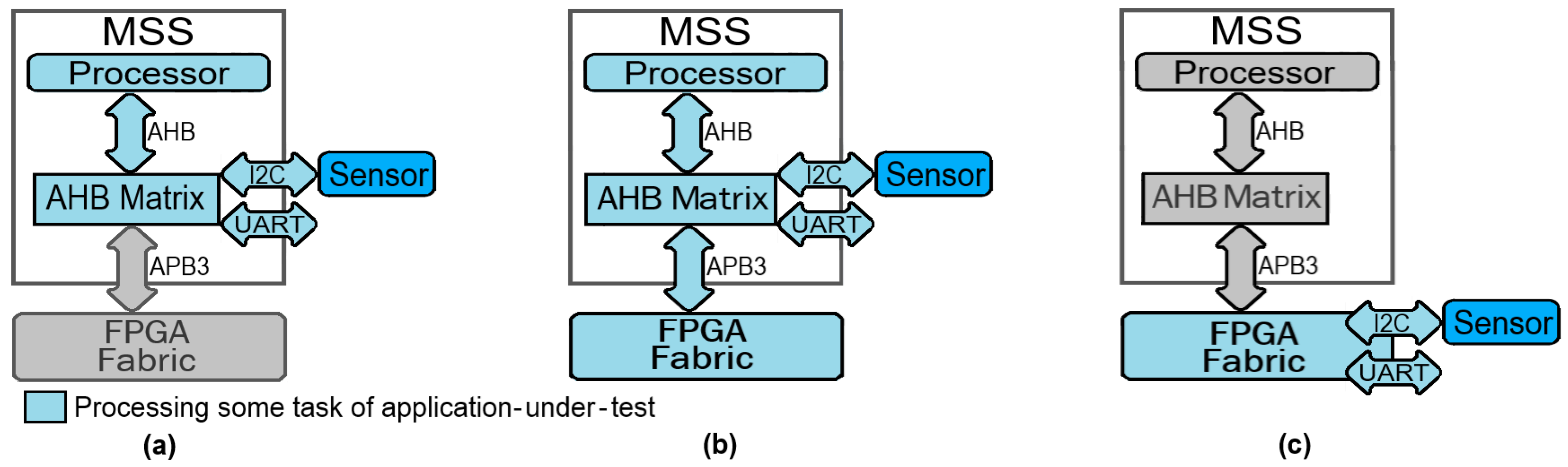
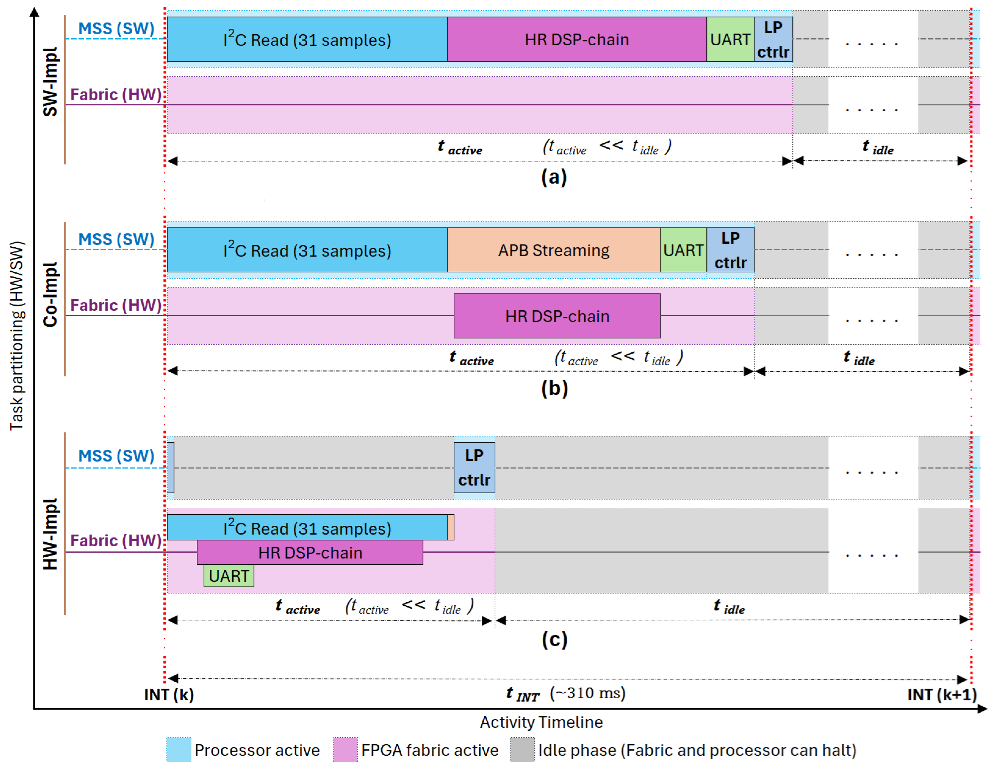
MSS-only Implementation (SW-Impl): The first implementation uses only the MSS subsystem of the SoC to provide a software baseline for the task-partitioning options available on Smartfusion2 SoC. All communication, signal-processing, and control run using the software on the embedded Cortex-M3 processor (hereafter called processor) via MSS peripherals, as seen in Figure 2a. Upon interruption from the sensor, the samples are read over an integrated MSS I2C interface. Each acquired frame is stored in a buffer and then processed by a HR DSP-chain. At the end of every third frame, the computed result is also transmitted over the MSS UART interface. The activity timeline, respective partition and duty cycle (active and idle phase) are shown in Figure 3a. In this implementation, the FPGA fabric is not used for any signal processing. However, during normal (non F*F) operation, the MSS CCC derives its reference clock (CLK_BASE) from a fabric CCC via the global clock network to generate aligned MSS clocks. Therefore, the fabric must remain active to keep this clocking path available while the MSS runs from these synthesized clocks. Since no user logic is implemented in the fabric in this baseline implementation, fabric activity is limited to the clocking resources required to supply CLK_BASE.
HW/SW Co-design (Co-Impl): In the second implementation, the application is realized as HW/SW co-design using both the MSS and the FPGA fabric, as shown in Figure 2b. The MSS is used for communication (I2C and UART) and LP modes’ control, while computationally intensive HR DSP-chain is offloaded to the FPGA fabric for speedup. The MSS acquires sample frames via its I2C module and transfers them to the FPGA over the APB bus for hardware-accelerated processing. The resulting estimate is then passed back to the MSS, which transmits it over UART. Initially, each sample was sent to the fabric for processing, and the result was read back against each sample, thus requiring two transfers per sample. To reduce this overhead, only the averaged result was transferred back to the MSS once per a 31-sample frame. It reduces APB transactions from 2 × n to n + 1 , where n is the number of samples per frame. Moreover, although each sensor sample is 18 bits wide, sending it over the 32-bit APB bus would normally require one full transfer per sample. To improve bus efficiency, we truncate each sample to 16 bits by discarding the two least significant bits (which lie below the noise floor) and pack two 16-bit samples into a single 32-bit APB word. It reduces the number of APB transactions per frame from 31 to 16. To accelerate this transfer further, the AHB bus matrix round-robin weight for this interface is set to 16.
This partitioning offloads only those parts of the workload which can benefit from fabric acceleration. The communication interfaces (e.g., I2C and UART) operate at fixed transfer rates, so their latency is largely insensitive to fabric speed-up. In contrast, the signal processing chain can benefit from hardware acceleration in the fabric. Such partitioning uses the FPGA’s parallelism to accelerate compute-intensive tasks, enabling race-to-idle behavior. This can reduce the active interval and total energy by increasing the time available for the LP mode. The activity timeline, respective partition and duty cycle (active and idle phase) are shown in Figure 3b.
HW Implementation (HW-Impl): The third implementation offloads the entire processing pipeline and communication interface controllers (i.e., I2C and UART) to the FPGA fabric, as depicted in Figure 2c. The MSS is limited to controlling entry and exit to/from LP modes in response to interrupts from the fabric. The FPGA fabric performs interrupt-driven data acquisition through its own I2C module. The DSP-chain is fully pipelined with the I2C acquisition. Unlike SW-Impl and Co-Impl, samples are not buffered as a complete frame before processing. Instead, each sample is passed to the DSP-chain as soon as it is acquired. After processing each frame, the result is transmitted over UART using lightweight logic. However, the result computed for frame k is transmitted in parallel to the processing of frame k + 1 . This overlaps communication with computation and further lowers end-to-end latency. Upon completion, the fabric issues an interrupt to the MSS, indicating the transition to the idle phase. The activity timeline, respective partition and duty cycle (active and idle phase) are shown in Figure 3c.
Since the MSS is limited only to control actions, as a result, the processor can enter sleep mode whenever it has no work, even while the fabric is actively processing, which reduces processor’s dynamic power. Moreover, implementing communication interface controllers in the fabric also allows application-specific interfaces, rather than using the full-featured hard MSS peripherals. Such tailored peripherals may reduce logic activity and resource consumption for a given workload; however, it is highly design-dependent.

3.3.2. Low-Power Mode Configurations

For each implementation, we evaluated five LP configurations against a no-LP baseline, resulting in six modes in total. All LP modes are applied during the idle phase, and power consumption is measured for different combinations of processor sleep, F*F, and processor standby clock settings. In HW-Impl, all tasks are executed in the fabric, and the processor is only required briefly at the end of the active phase to execute the configured LP mode. Consequently, the processor can remain in sleep not only during the idle phase but also for most of the active period when the fabric is processing. This enables three additional configurations. All the configurations are detailed in Table 1.
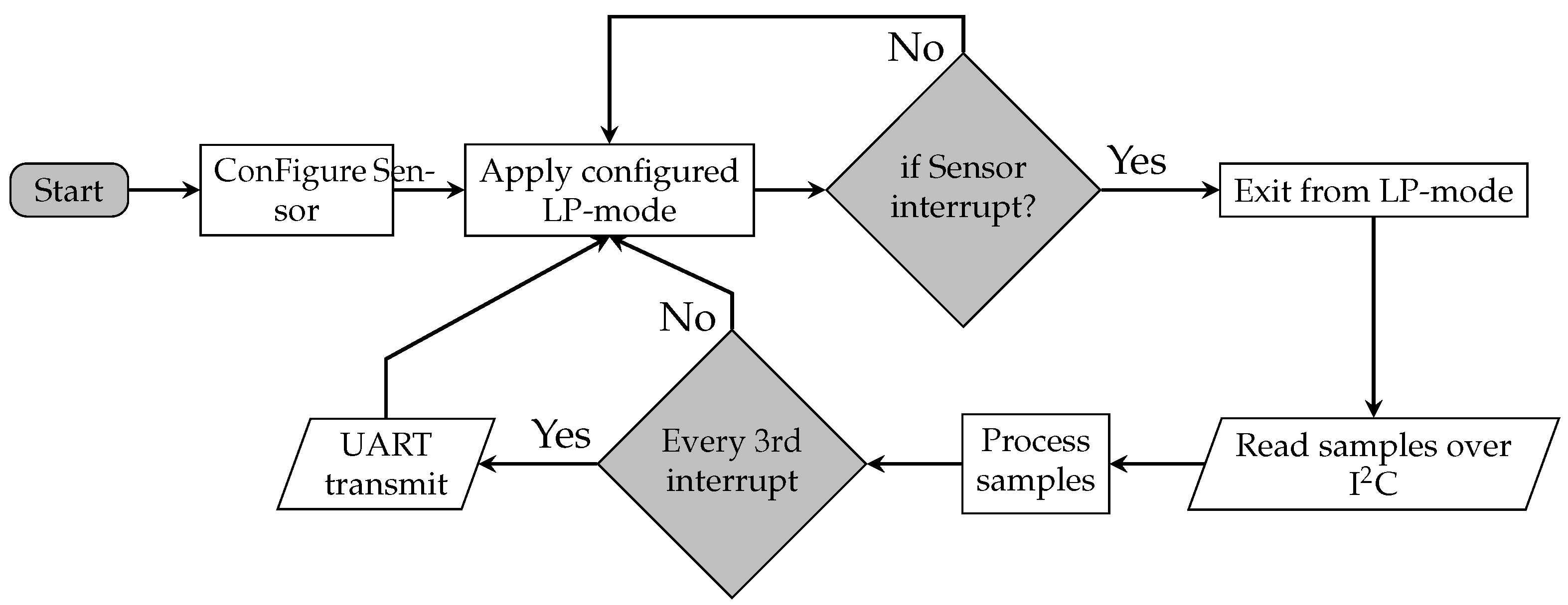
In all implementations, once the acquisition, computation and transmission are completed, the system returns to an idle state, waiting for the next interrupt from the sensor. The LP-ctrlr module, running at processor, executes the LP modes during this idle period. Different LP configurations are evaluated in this idle phase to assess their impact on reducing idle energy consumption. Figure 4 highlights the control flow of activities across the HR-monitoring application and LP-mode entry/exit phases.

3.3.3. Main Clock-Frequency Scaling

Changing the operating clock-frequency changes both the dynamic power consumption when the system is not in LP mode and the amount of time the system is in LP mode. In the SW and Co-Impl, communication with the sensor is implemented on the MSS using its I2C peripheral at 400 kHz. On MSS, the SCL rate is derived from the peripheral clock using a pre-scaler. However, the MSS I2C driver provides a discrete set of SCL pre-scalers, including 60, 120, and 224. Since the peripheral clock is derived from CLK_BASE (which is the main clock in our setup), we selected main-clock values of 24 MHz, 48 MHz, and 89.6 MHz to obtain an exact 400 kHz SCL from the available divisors. For experimental fairness, the same three main clock settings were used across all three implementations.

3.4. Experimental Setup and Power Measurement

The experiments use the SMF2000 (TEM0001) development board (Trenz Electronic GmbH, Hüllhorst, Germany) [50], built around a Microchip SmartFusion2 M2S010-VFG400 device (Microchip Technology Inc., Chandler, AZ, USA) [18]. A MAX30102 sensor (Analog Devices, Wilmington, MA, USA) [51], for pulse-oximetry and heart-rate, is used to acquire photoplethysmography (PPG) signals. Table 2 summarizes the sensor configuration used in all experiments. The sensor operates in FIFO-interrupt mode and triggers an interrupt when 31 new samples are available. The effective output data rate is 100 sps, yielding one event approximately every 310 ms. This event period defines the one-period window used for energy accounting in the Results section.
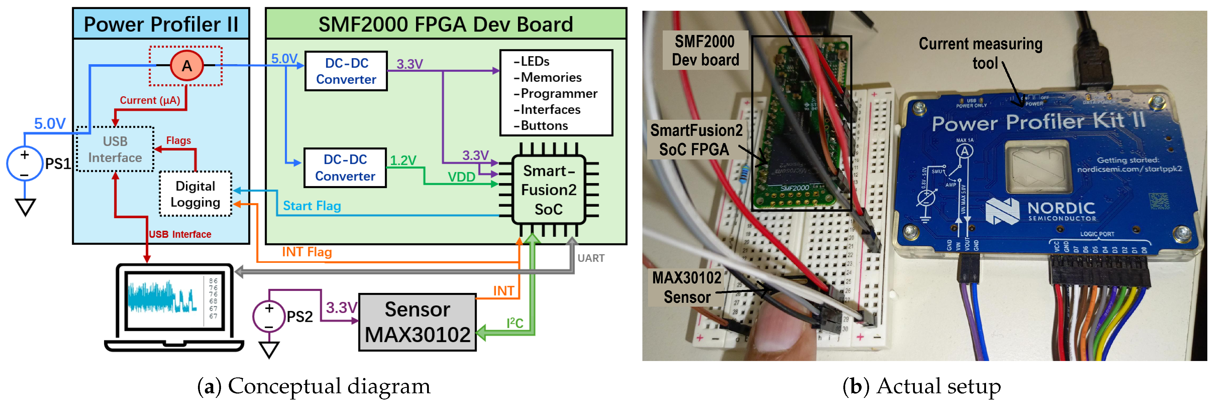
Power measurements are performed using Nordic Semiconductor’s Power Profiler Kit II (PPK2) (Nordic Semiconductor ASA, Trondheim, Norway) [52] in source mode, sampling the current at 100,000 samples per second. The sensor is connected to the development board via the I2C interface and an interrupt line; however, the sensor is powered separately from the FPGA development board (Figure 5a) to avoid mixing the sensor’s consumption with the FPGA board’s consumption. We did not measure the sensor power consumption in our experimental setup because the evaluated features (LP modes, frequency scaling, and task partitioning) do not change the sensor operating conditions.
Furthermore, since the FPGA development board does not provide a way to measure the FPGA current directly, isolating fabric-only consumption was not possible. We therefore report the power consumed by the whole development board. This board-level measurement includes the consumption of SoC FPGA as well as some consumption from other PCB components. To minimize unrelated consumption, we disabled non-essential components, such as LEDs. Additionally, the digital flags, such as start of activity, interrupt assertion, PLL’s locks, etc., were also logged to correlate power usage with corresponding events. The actual setup is shown in Figure 5b.

3.5. Robustness of Measurements and Analysis

For each implementations and its subsequent configurations, 40 s of current trace was recorded and repeated three times. We then extracted the first 100 periods from each run, yielding, in total, 300 periods per configuration. We computed and used the mean values of current and timing metrics (active, LP entry, LP exit, and idle) over these 300 periods. For fairness of comparison, we kept the PLL-related settings fixed across all runs, using default lock settings for the fabric PLL (lock window 32,000 ppm, lock delay 1024 cycles), while holding the output clock in reset until lock was acquired. Similarly, we kept the MSS MPLL settings default (lock window 8000 ppm and lock count 32 cycles). These parameters can affect the F*F exit latency and are therefore held constant. All FPGA designs were implemented in Libero-SoC v2024.1 (Microchip Technology Inc., Chandler, AZ, USA) [53], using power-driven place-and-route with a two-pass flow and a fixed seed. All firmwares were built in SoftConsole v2021.1 (Microchip Technology Inc., Chandler, AZ, USA) [54], using the release configuration, with compiler optimization set to −O2 (optimize more) and NDEBUG as the pre-processor macro.

3.6. Naming Convention

Since we evaluated a set of LP mode configurations across three implementations and multiple main clock frequencies, a naming convention was adopted to consistently identify the results. Each result is labeled as ImplName.MainClk_ConfigID. For example, a result corresponding to the Co-Impl operating at a 48 MHz main-clock, configured for the idle period as: fabric in F*F, standby clk 1 MHz, and processor in sleep, is denoted as Co48_F1_S.

4. Evaluation and Results

Firstly, in this section, the correctness of signal acquisition from the sensor and HR-monitoring algorithm is presented. Then, the energy efficiency of different LP configurations and implementations is analyzed and reported. The analysis also includes the impact of frequency scaling vs. LP mode configurations, on both latency and energy efficiency. Together, these results provide a comparison of the different design choices in terms of energy consumption, latency and duty cycle.

4.1. Verification of Used HR-Monitoring Algorithm

Although the goal of this work is to explore power-optimization strategies and analyze their impact on energy and latency in low-duty-cycle applications rather than to prove algorithm robustness, we nevertheless performed two functional sanity checks to confirm that the case-study algorithm behaves as intended.
In the first check, the algorithm’s functional correctness was evaluated using the PhysioNet BIDMC PPG & Respiration dataset [55]. Since we performed our power-measurement experiments in a lab environment while measuring HR in a resting state, the BIDMC dataset (collected in the resting state) was well-suited for functional-accuracy checks. Moreover, it provides PPG signals sampled at 125 Hz (close to our 100 Hz sampling rate) and includes reference HR values sampled once per second, enabling a direct comparison with our computed HR. From the dataset, each of the 53 PPG records (eight-minute each ≈ 60,001 samples each) was trimmed to 59,985 samples to fit our 31-sample frame, and we also re-tuned the beat acceptance window of our algorithm for the 125 Hz sampling rate. Since our HR algorithm requires 15–18 s to produce stable estimates due to its long averaging window, the first 15 s of results were excluded to ensure a fair comparison. The remaining HR estimates were then linearly interpolated to match the 1 s time grid of the reference HR, since our algorithm outputs one estimate every 0.744 s (93 samples), whereas the reference dataset provides values at 1 s intervals.
Using all 53 BIDMC recordings, the algorithm achieved an overall mean absolute error (MAE) = 2.72 BPM, root mean square error (RMSE) = 6.74 BPM, and bias = +1.49 BPM, with 87% of estimates within ±3 BPM of the reference, as detailed in Table 3. These numbers were inflated by a few outliers recordings that showed persistent offsets or irregular detections. After identifying and excluding five such recordings, while leaving the remaining 48, records unchanged, the overall performance improved to MAE = 1.61 BPM, RMSE = 2.52 BPM, and bias = +0.78 BPM, with 92% and 97% of estimates within ±3 BPM and ±5 BPM, respectively. These results demonstrate the functional correctness of the HR-monitoring case-study algorithm.
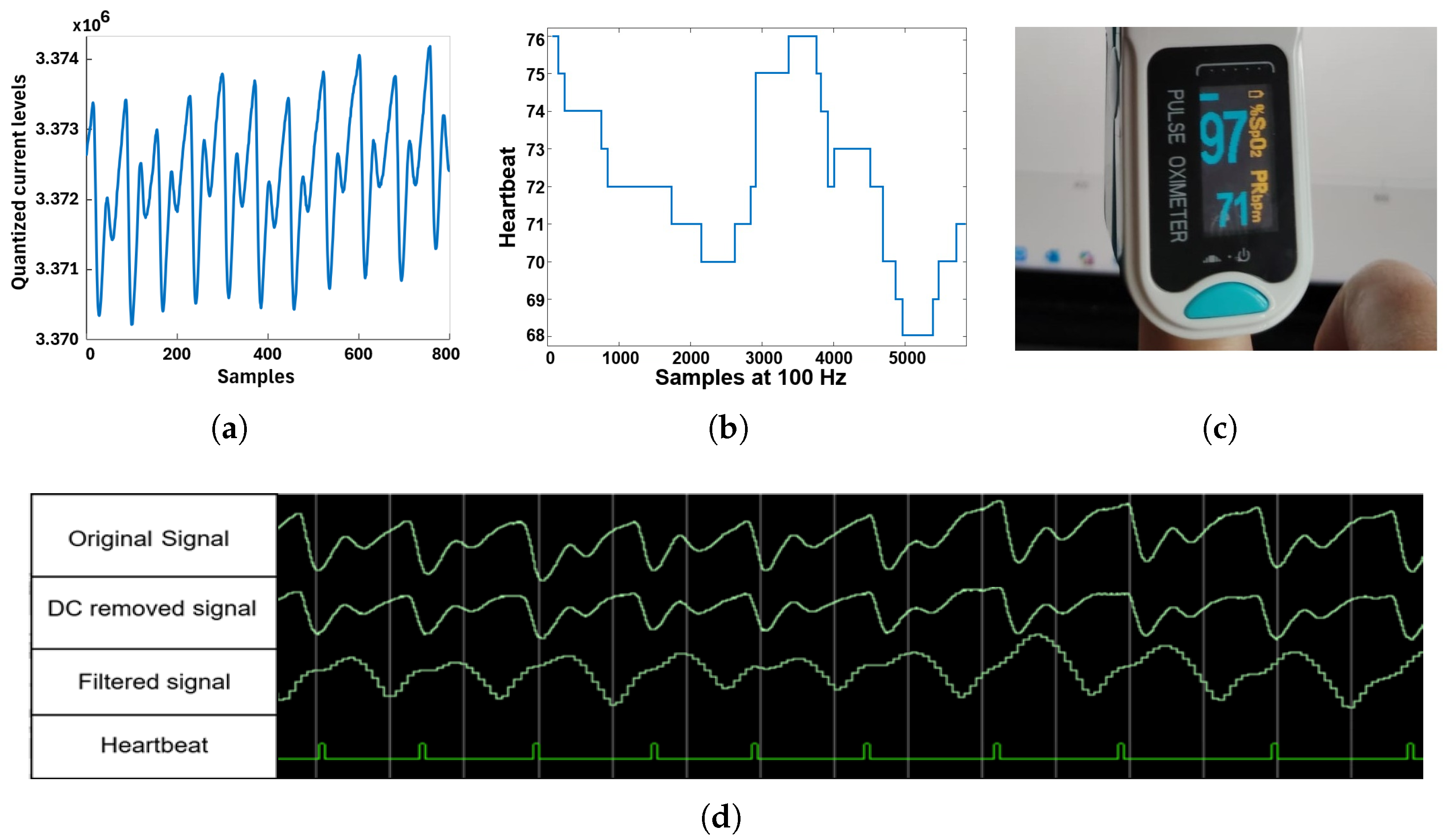
In the second check, we tested the functional correctness of our hardware with the HR algorithm deployed on it. The sensor was configured to acquire the PPG signal at 100 Hz (800 sps with averaging over 8 samples). After connecting the setup, a finger was placed on the sensor, and values were logged via a MATLAB (R2024b for Academic use) serial terminal over the UART interface. The logged signal, shown in Figure 6a, shows that our DAQ system preserves the key PPG features needed for heartbeat detection. The system’s HR values, with immediate validation using a medical pulse oximeter, are shown in Figure 6b,c. Additionally, for the FPGA-based accelerators, verification is shown via a ModelSim simulation in Figure 6d for heartbeat detection. Together, these results confirm the functional correctness of our sensing and processing pipeline on hardware as well.

4.2. Annotating Current Waveform with Different Operating Phases

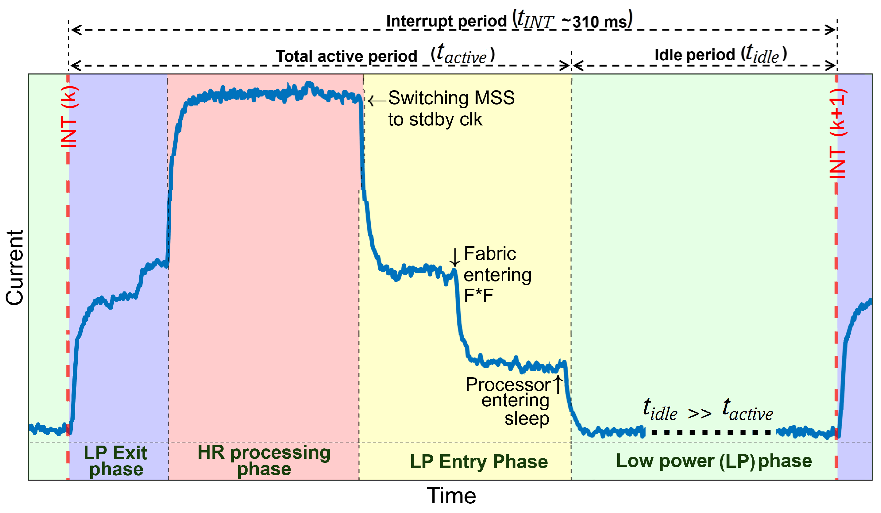
Before delving into the analysis of our results, we first explain how the measured current profile relates to different operating phases in one period. Figure 7 presents a current profile (edited for illustrative purpose) from SW-Impl where both F*F and sleep modes are applied during the idle phase with a standby clock of 1 MHz. The HW and Co-Impl also follow a similar current profile.
LP entry phase: This phase begins when the processor initiates an F*F request. The System-Controller first switches the MSS clock from the main clock (also called user clock) to the standby clock. It then powers down the fabric PLL/CCC and places the fabric into F*F. After F*F entry is completed, the processor enters sleep mode.
LP Exit phase: This phase starts upon the sensor’s interrupt. The processor wakes and initially runs on the standby clock while the System-Controller power-up clocking resources wait for the fabric PLL and MPLL to be locked. Once both are locked, the System-Controller switches the MSS clock from the standby clock back to the main clock. Until this switching is carried out, the processor keeps waiting for a lock status.
HR processing: Once switched, the processor starts executing the HR processing algorithm, which is a useful activity. These three phases are also collectively referred to as a total-active phase/period.
Idle/LP phase: The idle phase corresponds to the period where no activity is required to be performed, except for waiting for the next event. All evaluated LP configurations are applied during this phase. We also refer to the idle phase as the LP-phase when an LP configuration is active.
Therefore, the total power over one cycle can be categorized into P act (active), P idle (idle), P entry (low-power entry), and  P exit (low-power exit), while the total energy can be given as below.
E tot = P active · t active + P idle · t idle + P entry · t entry + P exit · t exit

4.3. Evaluation of LP Mode Configurations Across Implementations

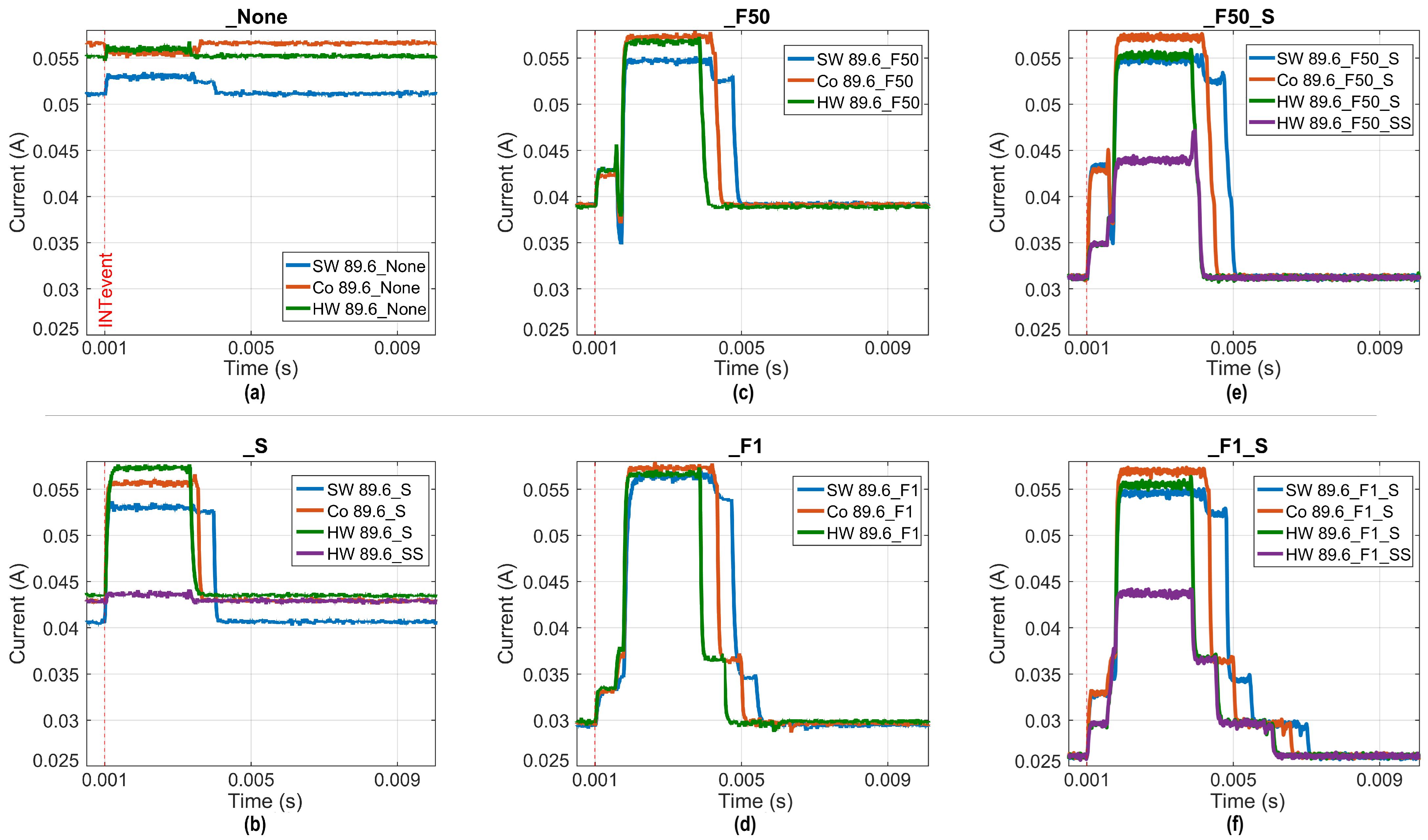
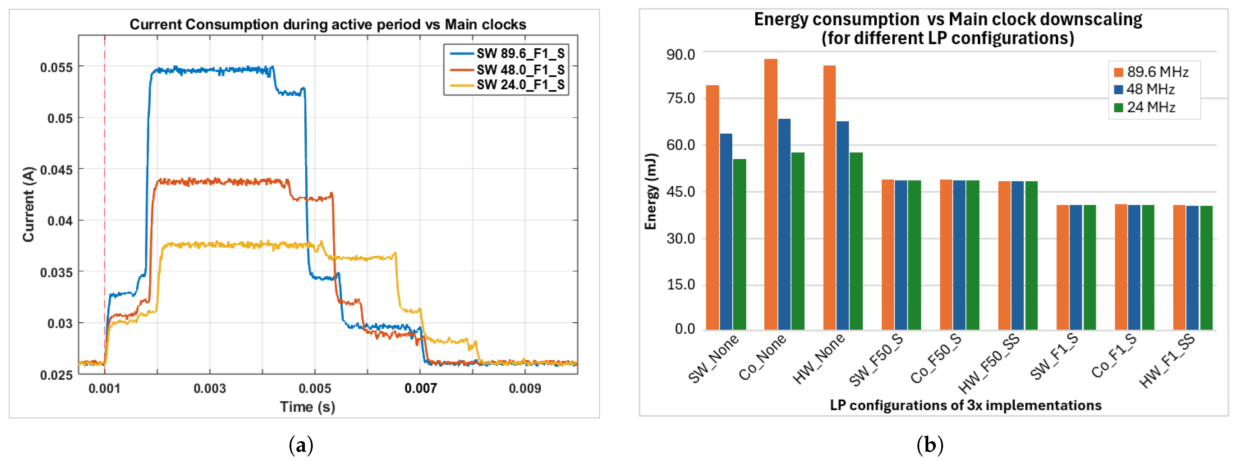
The current consumption measured for the three implementations, operating at a main clock of 89.6 MHz under different LP mode configurations, is presented in Figure 8. It compares the measured active- and idle-phase (LP-phase) current consumption of the three implementations under different LP configurations.
Idle-phase consumption: Across all implementations, the highest idle current is observed for the _None configuration, (Figure 8a), in which no LP mode is enabled. In this case, the SW-Impl exhibits the lowest idle current because no logic is instantiated in the FPGA fabric, whereas the Co-Impl and HW-Impl suffer additional consumption due to the presence of fabric modules. Placing only the processor to sleep mode during the idle phase (_S config) reduces the idle current in all implementations (Figure 8b). The SW-Impl continues to show the lowest idle current, as it does not have any fabric module. Relatively more reductions are achieved in _FF1 config where the fabric is placed in F*F while the processor remains active and operates from the 1 MHz standby clock (Figure 8d). Here, the idle current further decreases in all implementations as compared to the corresponding _S config. This occurs due to the fabric logic, CCCs, and associated PLLs being powered down, leaving only the MSS active. However, when the fabric is placed in F*F and the processor operates from the 50 MHz standby clock (_FF50 config), the idle current is higher than in the _FF1 case (Figure 8c). This is due to the fact that even when the processor is sleeping, the standby clock continues to drive always-on MSS logic (e.g., interrupt controller and any enabled peripherals), so a 50 MHz standby clock consumes more than 1 MHz. The lowest idle current is observed when F*F is combined with processor sleep (_FF1_S and _FF50_S). In these configurations, the fabric is in F*F while the processor is in sleep mode (Figure 8e,f). As expected, _FF1_S achieves a lower idle current than _FF50_S due to the lower standby clock frequency.
It is also worth noting that, for a given LP configuration, all three implementations exhibit nearly identical idle current consumption except in the _None and _S configurations. Here, the fabric is not placed in F*F and therefore remains powered during the idle phase, leading to an implementation-dependent idle current.
Active-phase consumption: During the active phase, the current consumption trends differ from those observed in the idle phase and depend on task partitioning. For the _None and _S configurations, the SW-Impl consumes less of the active current than the Co-Impl and HW-Impl (Figure 8a,b), since computation is performed entirely on the processor and no fabric logic is present. In contrast, the HW-Impl exhibits a significantly lower active current when the processor is also placed in sleep mode during the active phase while the fabric is busy due to processing. This behavior of HW-Impl is evident in its HW 89.6_SS config (Figure 8b) and becomes more prominent in HW89.6_FF1_SS (Figure 8f) and HW89.6_FF50_SS (Figure 8e) configurations, where the processor remains in sleep mode not only during idle periods but also for most of the active phase. As a result, in these HW-only configurations, the active-phase current of the HW implementation is lower than that of the corresponding SW and Co-Impl cases.
Furthermore, the entry and exit latencies with a 50 MHz standby clock are significantly shorter than a 1 MHz standby clock. This can be beneficial in very-high-duty-cycle applications where the idle intervals are very short. A 50 MHz standby clock is also advantageous in scenarios where only the fabric has idle periods, while the software on the processor must remain on and execute high-speed tasks that cannot be completed in time if the MSS is limited to 1 MHz before the next active period begins.
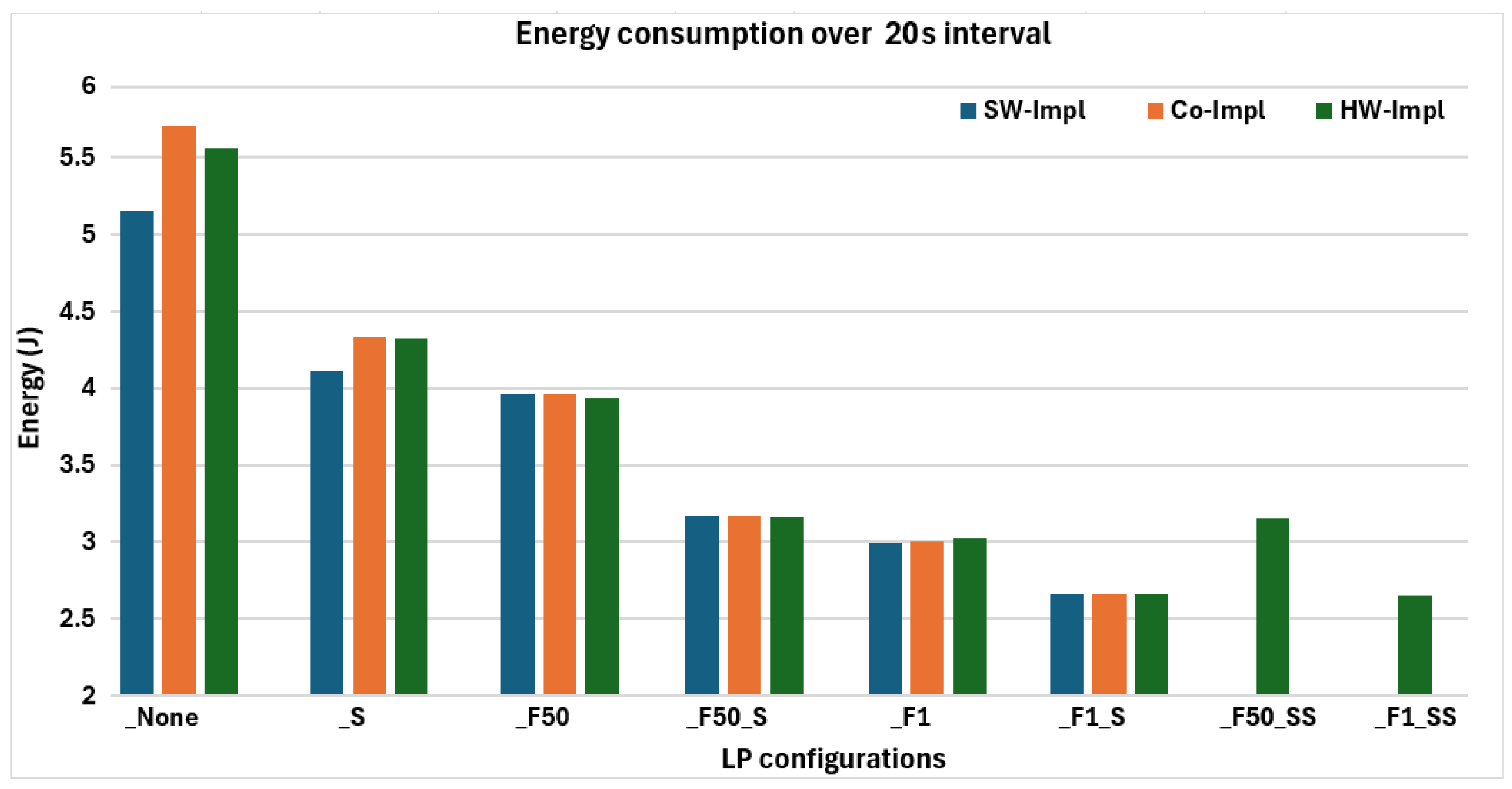
Figure 9 presents the energy consumption over a 20 s interval (corresponding to one stable HR estimate) for the three implementations under the different LP configurations. While the expected reduction in energy across LP configurations is noticeable, the energy difference between implementations for a given configuration is negligible, except for the _None and _S cases. This behavior is expected because of the very-low duty cycle (approximately 2%); hence, the total energy is dominated by the idle interval. The idle current, in those configurations, is nearly identical across implementations. Consequently, reductions achieved during the short active phase have a limited impact on the 20 s energy consumption. As the duty cycle increases, the active phase contribution grows and implementation-level differences become more noticeable. This trend is analyzed further in Section 4.5. Nevertheless, the best-performing LP configuration against SW and Co-Impl is _F1_S while for HW-Impl it is _F1_SS at standby clock of 1 MHz. Similarly, _F50_S for SW and Co-Impl while _F50_SS for HW-Impl at 50 MHz of standby clock. In the upcoming sections, we only used these best-performing configurations for further analysis. Finally, the resource consumption for each implementation is presented in Table 4.

4.4. Energy and Latency Trade-Offs Under Frequency Scaling

Since the LP configurations tested in the previous section focused on reducing the idle current, the lowest idle consumption was achieved when the FPGA fabric was placed in F*F and the processor was placed in sleep mode. In these configurations, the idle current is nearly identical across implementations because both the fabric and processor core clock are gated off during the idle phase. In such configurations, the remaining idle consumption is only due to a small set of always-on MSS blocks that operate from the standby clock and that are largely independent of the main clock. In contrast, during the active interval when the processor and/or fabric logic is running, the energy consumption depends on dynamic switching activity and therefore varies with the chosen main clock.
This section evaluates the impact of main clock-frequency downscaling on energy consumption and on the associated latencies. For each implementation, we selected the best-performing LP configurations identified in the previous section (one for each standby clock option). We also included _None as a baseline reference for comparison across frequencies.
Since dynamic power scales approximately as P dyn = α C V 2 f , downscaling the main clock reduces the active phase current consumption, as observed for the SW_Impl in Figure 10a. However, lowering the clock frequency increases the clock period and therefore extends the execution time of the software workload, leading to a longer active interval.
Figure 10b compares the energy per period for _None, _F1, _F50, _F1_S, _F1_SS, _F50_S and _F50_SS for three implementations for different main clocks. In the _None config, the energy decreases as the operating frequency is reduced. This happens because the processor and fabric modules remain clocked during the long idle interval. Reducing the clock therefore lowers dynamic consumption in the idle phase, and the effect becomes visible when looking at total energy consumption. In contrast, _F1_S, _F1_SS, _F50_S and _F50_SS show negligible energy reduction with frequency downscaling. In these configurations, the fabric is placed in F*F and the processor is in sleep during the idle phase. As a result, the idle energy is largely independent of the main clock. Although frequency downscaling reduces the active phase energy, the active interval contributes little to the total energy due to the very-low duty cycle. The overall energy therefore changes only slightly because it is dominated by the long idle period, whose consumption remains nearly constant across the tested frequencies.
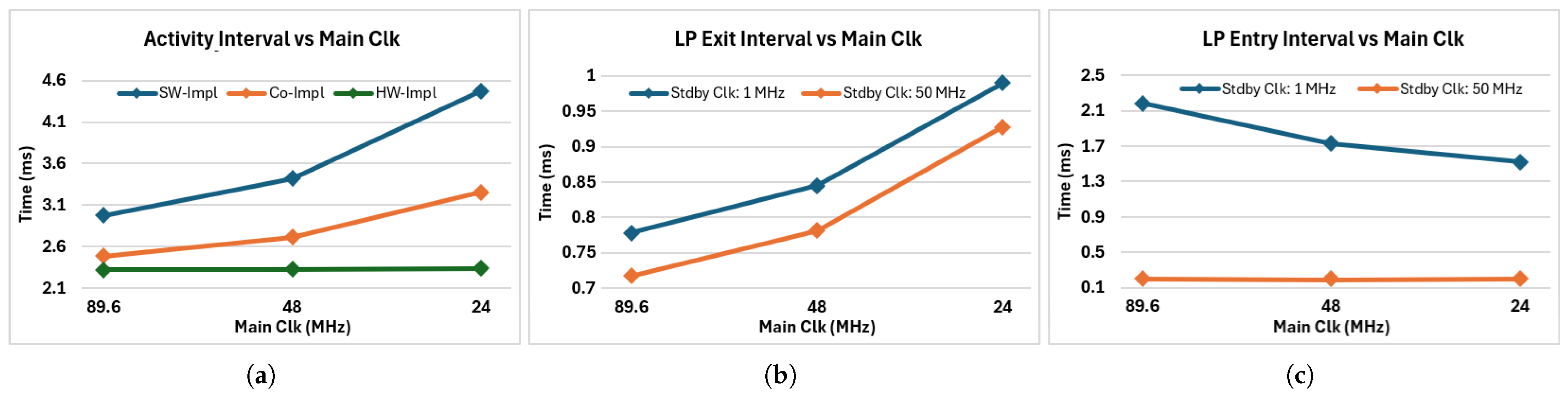
The trends of active time can be explained by the dominant communication interface latencies. The sample acquisition is constrained by data rate (400 kHz) of I2C bus, and the result reporting is constrained by the baud rate (115,200) of the UART.  Hence, the frequency downscaling mainly affects the HR DSP-chain computation time. From Figure 11a, it can be observed that this change is noticeable in the SW-Impl because the DSP-chain is implemented sequentially on the processor. However, in the Co-Impl, the DSP-chain runs in the fabric and processes each sample in nine clock cycles. As a result, the increase in computation time due to a lower clock frequency is small over one period. On the other hand, in the HW-Impl, the DSP-chain is fully pipelined with the I2C acquisition, so its operation is completed within the acquisition latency. The I2C module also performs an additional read of the sensor interrupt register to clear the interrupt. Consequently, the DSP-chain finishes before the I2C transaction ends; thereby, the frequency scaling effect on latency is not visible over the active period. Thus, there is a trade-off between the power consumption and active duty cycle. If the duty cycle is relaxed enough, a lower frequency can be used to save further power.
From Figure 10a, it can be seen that the LP-mode entry and exit latencies also change with the operating frequency of the processor. Entering and exiting the F*F also introduces some latencies. During F*F entry, the processor’s firmware first performs the required register configuration and then requests the System-Controller to place the fabric into F*F. The System-Controller switches the MSS clock from the main clock to the standby clock, powers down PLLs/CCCs, and notifies the firmware when the F*F entry sequence is complete. After receiving the “F*F done” notification, the firmware’s F*F routine returns and the processor executes sleep instructions. In this work, the LP entry interval is defined as the time from calling the firmware F*F routine to the execution of the sleep instructions. On an exit event (sensor interrupt), the System-Controller initiates the wake-up sequence by powering up the PLLs/CCCs and notifying the firmware via an interrupt. It then waits for the fabric PLL and MPLL to acquire a lock. Afterwards, it switches the MSS clock back to the main clock from the standby clock. Upon receiving the exit notification, the firmware exit routine concludes and returns. In this work, the LP exit interval is defined as the time from the external interrupt assertion to the return from the firmware F*F routine.
Since both LP entry and exit sequences involve some steps executed on the main clock and some on the standby clock, we evaluated these intervals across different main clocks for both standby clock options. Figure 11b shows that the F*F exit time increases slightly as the main clock decreases. The exit time is also consistently higher when using the 1 MHz standby clock than the 50 MHz standby clock. In contrast, the F*F entry time shows the opposite trend. Figure 11c indicates that the entry interval is larger at higher main clocks and smaller at lower clocks. This dependence is more pronounced with the 1 MHz standby clock and is negligible with the 50 MHz standby clock. The cause of the entry-time trend is not fully clear. However, the trend is consistent across repeated runs. One possible reason is that the System-Controller might need more time for a clean shutdown when the fabric is running at a higher frequency. However, we treated it as an empirical observation.
In LP-optimized configurations, frequency downscaling mainly reduces active-phase energy. Its impact on total period energy is therefore small due to the very-low duty cycle. In the next section, we evaluate how this behavior changes if the duty cycle or event rate increase and dominate the total period.

4.5. Effect of Event-Rate/Duty-Cycle Scaling on Energy Consumption

The HR-monitoring workload used in this work is lightweight and very-low-duty-cycle. In reality, the edge workloads could be more compute-intensive, and sensor characteristics may vary. These factors can increase the active time and thereby duty cycle, which can shift the energy-optimal operating point to another set of an LP configuration. One of the effects of a higher computational demand could be an increase in per-event processing (active) time, thereby increasing the duty cycle for a given event period. Likewise, the duty cycle could also increase due to having a different sensor type, having a different event rate (interrupt or sampling rate) or data volume per event (sample width, frame size, or number of channels), or a different interface transfer rate. For example, for a fixed interface rate, larger frames or more channels increase acquisition time and therefore increase the duty cycle. Similarly, a higher event rate lowers the event-period, thus reducing the available idle time and thereby increasing the duty cycle. This section analyzes the impact of a duty-cycle increase on energy consumption and operating-point selection using a scaling model.
In general, an increased duty cycle can be interpreted in two equivalent ways: (i) per-event active time increases for given event-period, or (ii) the event-rate increases which shortens the event-period. We adopt the second approach because it provides a simple way for us to study higher duty-cycle operations without changing the algorithm or sensor types. Instead of modifying the system under study and re-measuring at higher duty cycles, we extrapolated from the measured single-event case from the previous section. We assume that k identical events occur within the same 310 ms window, and that each event triggers a full cycle of activity followed by the F*F entry and exit phases. Under these assumptions, the measured currents and latencies from the previous section (k = 1 case) remain representative. Moreover, the total time spent in active and LP-entry/exit phases scales with k and thereby reflects an increased duty cycle.
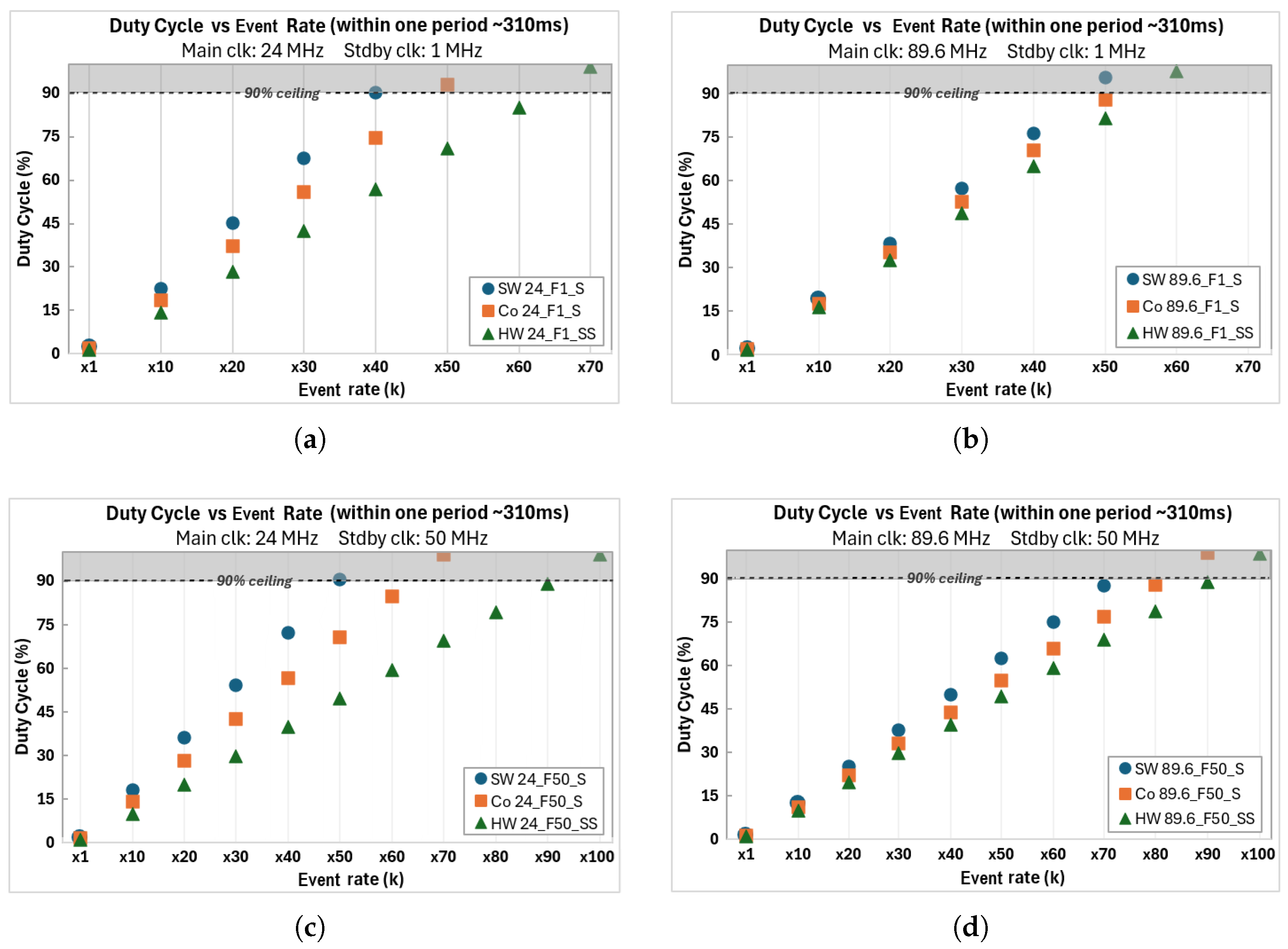
To determine the maximum feasible event rate k, we evaluated the best LP configuration from each implementation under both standby-clock options and across main clock-frequency scaling, as shown in Figure 12. We reserved at least 10% of the period for the idle phase. In our HR case study, each implementation has a different active time per event. Therefore, the same 310 ms window allows for different maximum k values. The baseline (k = 1) active time follows the trend t a c t i v e _ S W > t a c t i v e _ H E T > t a c t i v e _ H W . Therefore, SW-Impl supports a lower event rate than Co and HW-impl for the same clocking and LP configuration. The main clock also affects higher k feasibility. At lower main clocks, the active time per event is generally longer. This reduces the maximum feasible k. This can be observed for SW and Co-Impl from Figure 12a,b, where the maximum event rate is lower at 24 MHz than at 89.6 MHz. However, the HW implementation shows a different scaling trend across main clocks, i.e., a lower k at 89.6 MHz than at 24 MHz. This follows the same I/O-bound versus compute-bound behavior discussed in the previous section. In HW-Impl, the HR DSP-chain is pipelined with a sample reading process, so its latency is largely hidden under the I2C acquisition time. Therefore, the event interval is almost fixed and set by the fixed rates of the I2C and UART modules. Since the event interval in HW-Impl is almost independent of the main clock, the LP entry latency becomes more influential. As the measured LP entry time is higher at higher main clocks (Figure 11c), it can result in an increased total active time at higher frequencies and thereby reduce the maximum feasible k.
Since the F*F entry time limits the maximum feasible event rate, we also evaluated the 50 MHz standby clock option. With a 50 MHz standby clock, the firmware overhead during the entry routine is shorter, so the F*F entry latency is reduced. As a result, Figure 12c,d shows that a higher k becomes feasible due to a 50 MHz standby clock. It is also observed from Figure 12 that the difference between the maximum feasible k between the three implementations is larger at 24 MHz than at 89.6 MHz. At lower main clocks, the HR DSP-chain computation time is more visible in SW and Co-Impl and therefore differentiates the implementations more strongly. At higher main clocks, the DSP-chain latencies shrink and the fixed-rate I2C and UART latencies dominate. This reduces the difference in the total active time and makes the feasible k values be closer to each other. It can be inferred that when the application-processing interval is short and comparable to the F*F entry time, a 1 MHz standby clock can noticeably extend the total active time compared to a 50 MHz standby clock.
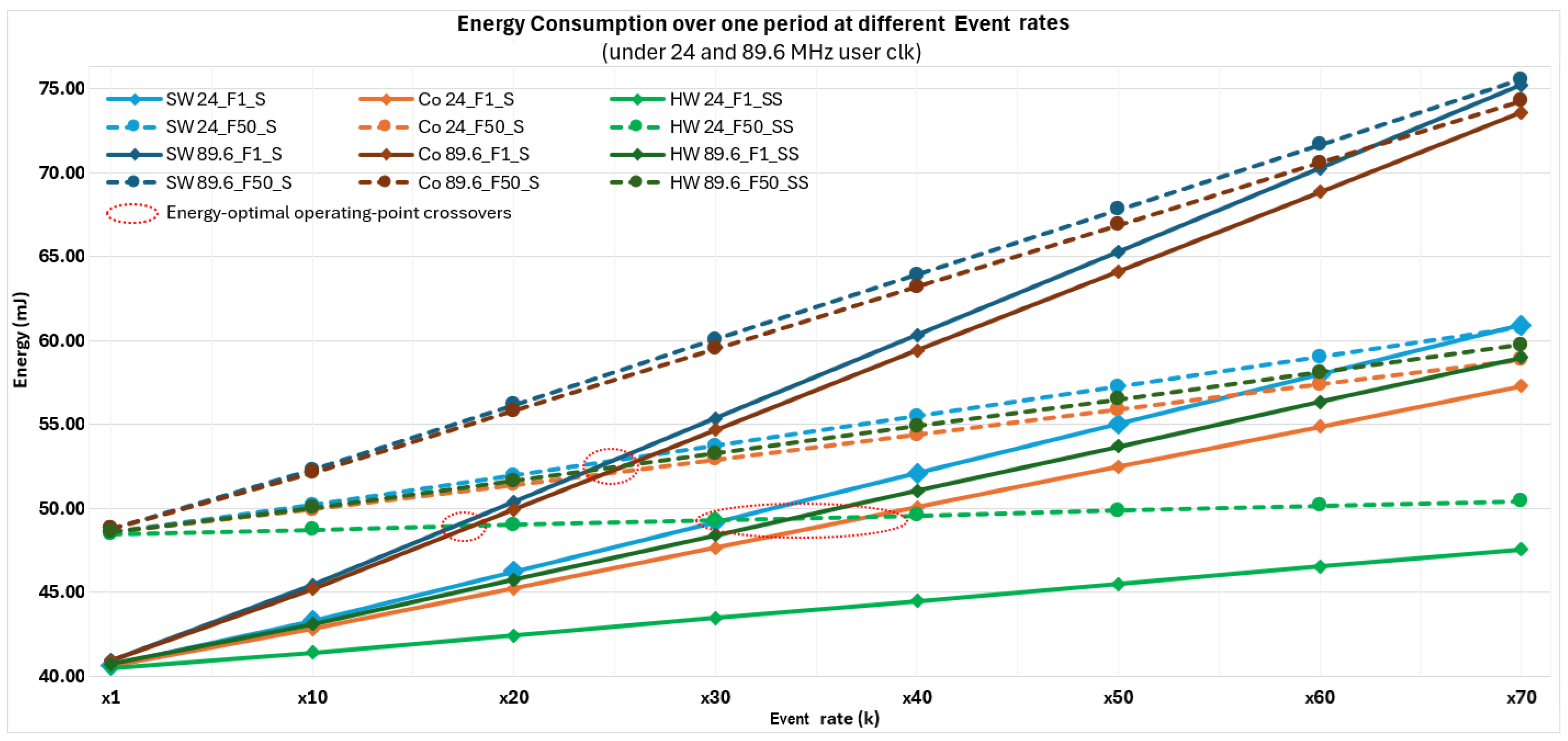
Next, we evaluated the energy consumption of the best LP configurations over event-rate scaling, against both standby clocks (50 Mhz and 1 MHz) and using two different main clocks (89.6 Mhz and 24 MHz), as shown in Figure 13. The observed energy consumption difference between a 50 MHz and 1 MHz standby clock for the same configurations (e.g., HW24_F1_SS and HW24_F50_SS) arises from the standby clock’s impact on transition overhead and the idle current. During the active phase, both configurations run from the main clock, so the active phase clocks are the same. The difference appears during F*F entry, exit and during idle phases, where the standby clock is used. A 1 MHz standby clock increases entry and exit latency, while a 50 MHz standby clock increases the idle current.
It can also be noted that at low event rates, the idle period dominates. Therefore, the standby clock choice has a strong impact on average power. In this case, the energy difference between the 1 MHz and 50 MHz standby configurations is large. As the event rate increases, the active and F*F transition intervals occupy a larger fraction of the 310 ms window and the idle time shrinks. As a result, the energy difference between the two configurations is reduced, as shown in Figure 13. At very high event rates, the idle time becomes comparable to the F*F entry/exit overhead. In this case, the energy benefit of a 1 MHz standby clock during an idle period becomes small. The 50 MHz standby clock can then be preferable because it reduces entry/exit latency and allows for a higher feasible event rate, with only a small penalty in average power.
Finally, Figure 13 also provides an insight into the best operating points as the event rate increases. For  k > 18 , HW 24_F50_SS yields lower energy than SW 89.6_F1_S and Co 89.6_F1_S. For  k > 25 , SW 24_F50_S, Co 24_F50_S, and HW 89.6_F50_SS also outperform SW 89.6_F1_S and Co 89.6_F1_S. For  k > 35 , HW 24_F50_SS further outperforms SW 24_F1_S, Co 24_F1_S, and HW 89.6_F1_SS. These results show that the optimal choice of implementation, standby clock, and the main clock depends on the event rate, and that selecting the appropriate operating point can reduce energy consumption.

5. Discussion and Guidelines

From Section 4.3, it is observed that, for low-duty-cycle workloads, the idle-phase energy consumption dominates the active-phase consumption. Therefore, the best strategy is to focus on applying the fabric F*F and processor sleep, as shown in Figure 8f. However, in practice, the edge application can have heavier computations, or different sensor characteristics (e.g., higher frame size), increasing the effective duty cycle. The duty-cycle scaling analysis in Section 4.4 shows that the active phase starts dominating with an increasing duty cycle; consequently, more effective optimization requires frequency scaling along with F*F and the sleep mode, as shown in Figure 13. In case the event rate increases due to higher sample rates or multimodal/multichannel sensors, the number of LP entry and exit transitions will also increase, making LP transition energy and latencies noticeable. In such cases, a configuration with a standby clock of 50 MHz can help reduce LP entry and exit latencies as well as energy, as indicated by Figure 11 and Figure 13.
In LP configurations where the fabric is placed in F*F and the processor is placed in sleep, idle consumption becomes nearly constant and largely independent of the main clock, as shown in Figure 8. As a result, frequency downscaling reduces the active-phase current, but its impact on period-level energy is small at a low duty cycle as observed from Figure 10a.
It is also observed from Section 4.3 that active-phase consumption depends on task partitioning choices. The SW-implementation executes sample acquisition, DSP-chain, and result reporting in software, so its active time is the largest, as seen from Figure 11a. The Co-implementation reduces the active time by moving the DSP-chain to the fabric for speedup, but the processor still performs sample acquisition and result reporting, which are transfer-rate-bound. The HW-implementation offloads sample acquisition, the DSP-chain and result reporting to the fabric. This allows the processor to remain in sleep mode during most of the active interval, which reduces the active current, as seen from Figure 8. Since this platform has the Cortex-M3 processor, it is modest compared to other advanced cores or independent MCUs. The active period latency and consumption on other platforms, having different processor cores, might appear differently.
The fixed-rate communication interfaces can also limit active-time scaling with frequency in low-duty-cycle applications. The I2C interface operates at 400 kHz, and UART transmission occurs at a fixed baud rate of 115,200. These I/O phases set a lower bound on active time. Therefore, frequency downscaling does not increase the end-to-end active interval in relation to the clock period. From Figure 11a, it can be observed that this effect is more visible in HW-implementations where the DSP-chain is pipelined with I/O interfaces. The main effect of frequency downscaling is a reduction in the active current (see Figure 10a, while the time impact depends on how much computation is serialized with serial interfaces.
The standby clock affects both transition overhead (LP entry and exit latency) and idle current consumption. A 1 MHz standby clock reduces idle current under the LP mode. However, it increases LP entry and exit latency, as shown in Figure 11b,c. A 50 MHz standby clock reduces entry/exit latency and supports higher event rates, but it increases the idle current under the LP mode, as seen from Figure 8e,f. This occurs because some always-on MSS parts remain clocked at this higher standby clock during processor sleep mode [20].
The energy-efficient operating point can shift with a higher event rate/duty-cycle. It can be observed from Section 4.5 that when the event rate increases (larger k), t i d l e shrinks and t a c t i v e becomes more significant. Under these conditions, the minimum-energy operating point can shift to the configurations that were not optimal at a low duty cycle. In particular, configurations using the 50 MHz standby clock can become preferable when entry/exit overhead limits feasibility or when wake-up latency is important, as seen from Figure 13.
Although we measured the current consumption of the whole FPGA development board (thus including DC–DC conversion losses from 5 V to 1.2 V and 3.3 V, as well as other PCB components and status LEDs), the results still show meaningful energy savings. From Figure 8f, we can notice that when the fabric is put into F*F and the processor into sleep mode, the board current in the idle phase reduces from ≈55 mA to ≈25 mA. The remaining ≈20 mA is due to always-on blocks of the SoC, static leakage, and other PCB components. This indicates that, even with fix baseline consumption, applying these low-power modes removes a large portion of the avoidable idle overhead.
Furthermore, since the heart-rate workload is lightweight, the idle energy wastage during the idle period is lower due to reduced resource utilization in the FPGA fabric. However, with an increasing computational demand, the resource utilization in the fabric increases, thus increasing not only the active consumption but also the idle consumption due to clocking and leakage of the additional logic resources. In such scenarios, the difference becomes even more pronounced when low-power modes are applied during the idle phase, resulting in further savings in idle energy consumption.
Moreover, from Figure 13, it can also be noticed that as the event rate/duty cycle increases, the difference in energy consumption among different task-partitioning variants also increases. For example, the energy consumption difference between SW_89.6_F1_S and HW_24_F1_SS at an event rate of k = 10 increases by 4× (from 1 mJ to 4 mJ). This awareness can therefore help lower a significant amount of energy consumption at higher duty cycles or event rates.
These savings justify the added complexity of LP modes’ application; however, the savings themselves are highly dependent on computational intensity and duty cycle.
The above findings are based on a low-duty-cycle workload running on the SmartFusion2 SoC platform and can be generalized to similar platforms for low-duty-cycle workloads. Although the idea of duty-cycle-aware application of low-power modes can be applied to SRAM-based FPGAs, a direct comparison is not straightforward. In SRAM-based FPGAs, power gating typically clears the configuration memory. Therefore, recovering from a power-gated state requires reconfiguration, which adds extra latency and energy overheads during the low-power exit phase. As a result, (i) the effective duty cycle becomes more sensitive to the LP-exit phase due to a higher reconfiguration latency, and (ii) the net energy saving from power gating becomes more sensitive to the LP-exit phase due to reconfiguration energy, as part of the “saved” idle energy is wasted by reconfiguration energy. Furthermore, the reconfiguration overhead also depends on bitstream size. Nonetheless, duty-cycle-aware application of low-power modes can still be beneficial on SRAM-based FPGAs in applications where (i) the duty cycle is low enough to tolerate the reconfiguration latency, and (ii) the reconfiguration energy overhead is sufficiently lower than the savings achieved through power gating.
On the other hand, the heart-rate monitoring workload is a very low-duty-cycle application. In practice, an edge application can have heavier computations or different sensor characteristics (sampling/interrupt rate, sample width, frame size, interface transfer rate), increasing the effective duty cycle. We compensate for this with duty-cycle scaling analysis to provide an insight into higher-duty-cycle applications. Furthermore, a higher computational demand can also increase per-event active current by activating more resources or increasing switching activity. In such cases, the event-rate scaling model does not directly predict new energy values; however, the qualitative guidance from the duty-cycle scaling analysis still applies. Although the active-phase energy will be higher for compute-intensive algorithms, the same trend holds: when the active phase becomes a larger fraction of the period, the energy-optimal operating point can shift to a different configuration.

Guidelines

Finally, we propose the following guidelines, which can be applied as a decision process. The reader can start from the application duty cycle and latency requirements, and then select the most suitable operating point.
  • Minimize idle energy first for low-duty-cycle workloads: If the application spends most of its time being idle, prioritize configurations that place the fabric in F*F and the processor in sleep mode (e.g., _F1_S or _F50_S), as demonstrated in Figure 8e,f. In this regime, changes in the main clock have a small effect on period-level energy, as seen in Figure 10b, because the idle phase dominates.
  • Choose the standby clock based on wake-up latency and idle duration: If long idle intervals are expected and wake-up latency is not strict, use a 1 MHz standby clock to minimize idle current, as demonstrated in Figure 10b. If wake-up latency is critical or idle intervals are short due to a higher event rate or duty-cycle, use a 50 MHz standby clock to reduce LP entry and exit time, as observed from Figure 11b,c. The event-rate scaling analysis from Figure 13 shows that the energy penalty of switching from a 1 MHz standby clock to a 50 MHz standby clock becomes small at high event rates because the idle time is reduced.
  • Use frequency downscaling when active energy matters: Main-clock downscaling reduces the active current, as observed from Figure 10a. It provides the most benefit when active time is a significant fraction of the period, as demonstrated in Figure 13. This occurs at higher event rates, or when computation dominates the active interval. For very-low duty cycles, frequency downscaling may not noticeably reduce energy per period even if the active current decreases.
  • Prefer Co or HW-Impl when compute-bound tasks dominates: If the workload includes significant computation, moving the DSP-chain to the fabric reduces the active time and can reduce energy. From Figure 11a, it can be observed that Co-Impl provides a middle ground in terms of active time reduction while HW-Impl offers the lowest active time.
  • If the interface dominates active period, optimize the LP and idle phases: When the workload is bounded by fixed-rate I/O interfaces, e.g., I2C or UART transfers, changing the main clock has a limited impact on end-to-end active time, as explained in Section 4.4. In this case, focus on reducing the LP transition overhead and idle current. Use a 50 MHz standby clock if frequent transitions are required, and a 1 MHz standby clock if the idle period dominates, as demonstrated in Figure 13.
  • Check feasibility at high event rates: For increased event-rate scenarios, verify that the schedule fits within the period budget, as observed from Figure 12. If the configuration becomes infeasible to fit within the period, switch to an operating point with a (i) lower transition overhead, e.g., a 50 MHz standby clock (Figure 11c),  (ii) a faster main clock, or (iii) an implementation with more acceleration from FPGA fabric (Figure 11a).

6. Conclusions

Currently, energy-constrained edge systems are required to offer both reconfigurability and higher computational capability to accommodate rapidly evolving and growing workloads. Flash-based SoC FPGAs offer an attractive middle ground by combining reconfigurable acceleration with LP modes. However, the most energy-efficient operating point depends on how these LP modes interact with HW/SW task partitioning and clock scaling. In this work, we comparatively evaluated the effect of these interactions on energy consumption and latency using a sensor-driven heart-rate monitoring application on Smartfusion2 SoC FPGAs. We evaluated the impact of F*F, processor sleep and standby-clock selection on SW, Co, and HW implementations in terms of energy consumption and latencies.
For the measured low-duty-cycle workload, total energy is dominated by idle consumption, and the lowest energy is achieved by combining fabric F*F with processor sleep. Task partitioning mainly effects the active phase by changing active time; however, its effect is negligible on period-level energy under very-low duty cycles. Similarly, although main-clock downscaling reduces the active current, it still yields a limited reduction in total energy per period for low-duty-cycle workloads. Moreover, the variation in active-phase time under frequency scaling is also limited when fixed-rate I/O dominates the active period. The standby clock presents a clear trade-off: 1 MHz minimizes the idle current, while 50 MHz reduces entry/exit latency and enables higher feasible event rates. Using a scaling model, we also observed that the energy-optimal operating point can shift as the event rate increases, and operating-point selection should therefore consider duty-cycle and latency constraints. The presented results provide practical guidelines for choosing an energy-efficient configuration across implementation styles, standby clocks, and main clocks on similar flash-based SoC FPGAs. As future work, we plan to validate these findings on other FPGA types with computationally intensive workloads.

Author Contributions

Conceptualization, B.d.S. and M.I.K.; methodology, M.I.K.; measurements, formal analysis and investigation, M.I.K. and N.R.B.M.; writing—final draft preparation, M.I.K.; review, A.N., A.S. and B.d.S.; editing, M.I.K.; supervision, B.d.S. All authors have read and agreed to the published version of the manuscript.

Funding

This research was supported through a Ph.D. scholarship from Pakistan and through the project “Power-efficient Artificial Intelligence for Biomedical Applications” (OZR4103) at the Vrije Universiteit Brussel.

Data Availability Statement

The data supporting the reported results can be made available upon request. The verification of the HR algorithm was completed using a publicly available dataset.

Acknowledgments

During the preparation of this manuscript/study, the author used ChatGPT-5 (5.4 Thinking) for the purposes of text editing, including grammar, spelling, punctuation, formatting, and reorganizing sentences/paragraphs to improve the flow and clarity of text. It was used solely as a writing assistant and was not used for analyses, discussion, or original intellectual ideas. All outputs were reviewed and corrected/edited (if necessary). The authors approve and take full responsibility for the content of this publication.

Conflicts of Interest

The authors declare no conflicts of interest.

Abbreviations

The following abbreviations are used in this manuscript:
ADCAnalog to digital converter
ASICApplication Specific Integrated Circuits
CCCClock conditioning circuits
clkClock
Co-designHW/SW co-design
DSPDigital Signal Processors
DSP-chainA chain of digital signal processing modules
F*FFlash*Freeze
FPGAsField-programmable gate arrays
freqFrequency
GPPGeneral purpose Processors
GPUGraphic Processing Units
HRHeart-rate
HWHardware
I2CInter-integrated circuit
IBS(Number of) inter-beat samples
IoTInternet of things
IRInfrared
LEDLight emitting diode
LPLow-power
LP-ctrlrLow-power controller
MCUMicrocontroller
MSSMicrocontroller subsystem
PLLPhase-locked loop
PPGPhotoplethysmography
SoCSystem-on chip
stdbyStandby
SWSoftware

Appendix A. Microchip’s SmartFusion2 SoC FPGA Platform

In this work, we have used SMF2000 (TEM0001) FPGA development board (Figure 5b) from Trenz Electronic [50]. It is a compact, low-cost module built around a Microchip SmartFusion2 SoC M2S010-VFG400 FPGA and a single power supply input. The input power lane is further split into two power buses using DC-DC converters: a 3.3 V bus and a 1.2 V bus (VCCINT). The VCCINT bus feeds the FPGA core, while the remaining FPGA rails are powered from the 3.3 V bus. The SmartFusion2 SoC integrates three main subsystems: (i) ARM Cortex-M3-based microcontroller subsystem (MSS), comprising the processor core, buses, memories and peripherals (ii) flash-based 12-kLUT FPGA-fabric and (iii) System-Controller responsible for executing F*F and some other services. Power consumption of SmartFusion2 SoC FPGAs can be managed through appropriate standby clock selection, putting fabric to F*F through System Controller, and processor sleep mode.

Appendix A.1. Clocking and Standby Operation

SmartFusion2 SoC devices provide two on-chip RC oscillators (50 MHz and 1 MHz) along with crystal oscillators. These sources can feed the on-chip Clock Conditioning Circuits (CCCs) to generate clocks of various frequencies/phases for the MSS and fabric [21]. Each CCC includes a dedicated PLL (phase locked loop) for clock synthesis and synchronization. Along with fabric CCCs and their associated PLLs, the SoC also contains a dedicated CCC for the MSS clocking (MSS CCC) having its own PLL (MPLL). The MSS CCC uses a base reference clock, supplied from a fabric CCC via the fabric global network, to synthesize the aligned MSS clocks. However, during F*F mode when fabric CCC & PLLs are powered down, one of the on-chip RC oscillators can be configured as standby clock source to MSS. The choice of appropriate standby clock can significantly impact energy consumption.

Appendix A.2. System-Controller and Fabric Flash*Freeze:

The System-Controller is an on-chip management block that executes system services such as device programming, F*F, cryptographic functions, etc. [56]. In this work, we evaluated the F*F service. F*F mode is a low-power state designed to significantly reduce power consumption by shutting down most system clocks and halting the FPGA fabric, while still retaining the contents of SRAM, registers, and I/O states. It is ideal for applications that require very low standby power without losing system context.
F*F request can be initiated either by processor firmware or fabric master, through an F*F service request to the System-Controller. In response, the System-Controller powers down the fabric PLL and CCC while retaining their configuration state; runs the MSS on the internal RC oscillator (50 MHz or 1 MHz); powers down the FPGA fabric while preserving register contents in suspend latches; and powers down Math_blocks while retaining their state [23]. The system can exit F*F through previously configured wake up events such as an I/O activity, RTC timeouts, or other interrupts, after which the System-Controller restores the clocks and resumes normal operation. This mode is enabled because of the non volatility of flash transistors which allow them to retain information even without power supply, thus the F*F mode power gates the fabric drastically reducing leakage.

Appendix A.3. Processor Sleep Mode:

The ARM Cortex-M3 processor also supports sleep mode, in which the core clock is gated off while maintaining the state required for rapid wake-up [19]. The interrupt controller remains active, allowing the processor to quickly resume execution upon an interrupt.

Appendix B. Heart-Rate Monitoring Workload

PPG-based heart-rate monitoring, widely used in wearables (e.g., smartwatches), is used as a representative low-duty-cycle case study. Its periodic and interrupt-driven behavior produces a clear active–idle structure: acquisition and processing phase followed by long idle interval. The workload also includes both transfer-rate-limited tasks (I2C and UART) and compute-bound signal-processing tasks. Above characteristics makes it suitable for studying low-power modes, clock scaling and HW/SW partitioning.
For heartbeat detection, we adopt publicly available algorithm from the MAX3010x sensor library [49], with minor tweaks to make it hardware-friendly. The full datapath consists of an I2C module, HR-monitoring digital processing chain (HR DSP-chain), a UART module and a low-power controller (LP-ctrlr) as shown in Figure 1. The I2C module provides communication channel to configure the sensor and reading PPG samples from it. These samples are then processed by HR DSP-chain consisting of the following modules:
DC remover: A PPG signal generally consists of two parts: a large DC-component (arising from tissue, skin and constant blood volume) and a small AC-component (corresponding to the pulsatile changes with each heartbeat). To isolate the AC-component, the slow-varying DC baseline is estimated using an Exponentially Weighted Moving Average, a first-order IIR low-pass filter. This baseline estimate is then subtracted from the raw PPG signal, leaving the AC component that reflects the pulsatile heartbeat activity.
PPG DC [ n ] = α · PPG raw [ n ] + ( 1 α ) · PPG DC [ n 1 ]
PPG AC [ n ] = PPG raw [ n ] PPG DC [ n ]
FIR filter: After DC removal a finite impulse response (FIR) filter is applied to further smooth the pulsatile waveform and suppress high-frequency noise. However, in HW-Impl, the same filter is realized in transposed direct form, adapted from [57], enabling all multiplications and additions to be performed concurrently. This parallelization exploits the FPGA’s dedicated DSP slices, ensuring high throughput and efficient real-time operation.
HB detector: Beat detection utilizes a zero-baseline crossing/threshold test combined with local peak–valley checks to confirm sufficient amplitude. If the signal is within a threshold, then it is considered to have a heartbeat. Heartbeat detection is not the same as a HR calculation as this also requires to know the time locality of the pulses.
IBS calculator: We computed the inter-beat interval as sample-count instead of using timer-based timestamps. This approach is equivalent, in principle, to timer-based measurement but avoids separate timer interrupts that could unnecessarily wake the processor from sleep mode. The Sample-counter measures inter-beat interval directly in sample-domain by counting the number of samples between two successive accepted heartbeats. We denote this value as inter-beat samples (IBS). The Averager module improves robustness against noise and false or missed detections. It rejects IBS values corresponding to unrealistically short or long beat intervals. It then applies a moving average over the 16 most recent valid IBS values to further smooth any sharp beat-to-beat variability.
Instead of computing beats-per-minute (BPM) on the device and transmitting the heart-rate value, this system directly transmits the averaged IBS value over UART. BPM conversion is therefore offloaded to receiver-side which can compute
BPM = 60 IBS · T s
using already known sensor’s sampling period T s . Such approach avoids division operations on the device. This reduces computational cost and thus allow implementation on a resource-constrained hardware.
After completing these processes and transmitting the IBS value over UART the system returns to an idle state, waiting for the next interrupt from sensor. The LP-ctrlr then executes the configured LP modes during this idle period.
Duty-cycle of HR application: The sensor operates in FIFO-interrupt mode, such that it generates an interrupt when 31 new samples are available in its FIFO. The sensor’s sampling rate is set to 400 samples/s, and its sample averaging is configured to 4 samples, resulting in an effective output data rate of 100 samples/s at its FIFO. Consequently, the sensor generates an interrupt every 310 ms, which is the time required to accumulate 31 new samples at 100 Hz. Upon each interrupt, the active-period starts and the system responds by reading these samples over I2C, processing them for heartbeat detection and transmitting the resulting IBS value over UART. After completing these processes, the system returns to idle-period, waiting for the next interrupt. The duty cycle can be observed from Figure 3.

Appendix C. PPG Sensor—MAX30102

The MAX30102 is an integrated pulse-oximetry and heart-rate sensor intended for wearable and portable health devices [51]. It uses PPG, a non-invasive optical technique, to measures blood volume changes. Light from the sensor’s LED penetrates tissue and is partially absorbed by blood. With each heartbeat, arterial blood volume changes, modulating the reflected light which is picked and translated to current variations by sensor’s photo diode. These current oscillations are sampled and buffered in internal 32-sample FIFO. The sensor provides a programmable FIFO almost-full interrupt threshold (17–31 samples) and an optional FIFO rollover mode. These features help prevent FIFO overflow and notify the host to read out samples in time. It also exposes other configurable parameters such as sampling rate and averaging, LED pulse width and current, ADC resolution and dynamic range, etc. Sensor provides an I2C interface for configuration and samples read out. It also provides a dedicated interrupt pin that asserts when the FIFO reaches the programmed threshold. In this work, that interrupt is used to trigger the processing system to fetch the newly available samples.

References

  1. Shumba, A.T.; Montanaro, T.; Sergi, I.; Bramanti, A.; Ciccarelli, M.; Rispoli, A.; Carrizzo, A.; De Vittorio, M.; Patrono, L. Wearable Technologies and AI at the Far Edge for Chronic Heart Failure Prevention and Management: A Systematic Review and Prospects. Sensors 2023, 23, 6896. [Google Scholar] [CrossRef]
  2. Chen, R.; Zhang, H.; Ma, Y.; Chen, J.; Yu, J.; Wang, K. eSSpMV: An embedded-FPGA-based hardware accelerator for symmetric sparse matrix-vector multiplication. In Proceedings of the 2023 IEEE International Symposium on Circuits and Systems (ISCAS), Monterey, CA, USA, 21–25 May 2023; pp. 1–5. [Google Scholar] [CrossRef]
  3. Su, X.; An, L.; Cheng, Z.; Weng, Y. Cloud–edge collaboration-based bi-level optimal scheduling for intelligent healthcare systems. Future Gener. Comput. Syst. 2023, 141, 28–39. [Google Scholar] [CrossRef]
  4. Covi, E.; Donati, E.; Liang, X.; Kappel, D.; Heidari, H.; Payvand, M.; Wang, W. Adaptive extreme edge computing for wearable devices. Front. Neurosci. 2021, 15, 611300. [Google Scholar] [CrossRef] [PubMed]
  5. Liang, Y.; Zhao, C.Z.; Yuan, H.; Chen, Y.; Zhang, W.; Huang, J.Q.; Yu, D.; Liu, Y.; Titirici, M.M.; Chueh, Y.L.; et al. A review of rechargeable batteries for portable electronic devices. InfoMat 2019, 1, 6–32. [Google Scholar] [CrossRef]
  6. EU. Next Generation Power Sources for Self-sustainable Devices—Integrated Multi-source Energy Harvesters. 2023. Available online: https://cordis.europa.eu/project/id/705437 (accessed on 4 March 2024).
  7. Singh, P.; Pandey, B.; Bhandari, N.; Bisht, S.; Bisht, N.; Budhani, S.K. Design of Energy Efficient IoMT Electrocardiogram (ECG) Machine on 28 nm FPGA. In Towards the Integration of IoT, Cloud and Big Data: Services, Applications and Standards; Rishiwal, V., Kumar, P., Tomar, A., Malarvizhi Kumar, P., Eds.; Springer Nature: Singapore, 2023; pp. 43–55. [Google Scholar] [CrossRef]
  8. Raza, K.; Samadi, A.F.; Berecibar, M.; Hosen, M.S. From EV to stationary energy storage: EIS-based SoH estimation for second life Li-ion batteries. J. Energy Storage 2026, 141, 119316. [Google Scholar] [CrossRef]
  9. Chen, R.; Zhang, H.; Li, S.; Tang, E.; Yu, J.; Wang, K. Graph-OPU: A Highly Integrated FPGA-Based Overlay Processor for Graph Neural Networks. In Proceedings of the 2023 33rd International Conference on Field-Programmable Logic and Applications (FPL), Gothenburg, Sweden, 4–8 September 2023; pp. 228–234. [Google Scholar] [CrossRef]
  10. Tesema, W.; Jimma, W.; Khan, M.I.; Stiens, J.; da Silva, B. A Taxonomy of Low-Power Techniques in Wearable Medical Devices for Healthcare Applications. Electronics 2024, 13, 3097. [Google Scholar] [CrossRef]
  11. Actel. The Many Flavors of Low-Power, Low-Cost FPGAs. Available online: https://ww1.microchip.com/downloads/aemDocuments/documents/FPGA/ProductDocuments/SupportingCollateral/low_power_wp.pdf (accessed on 10 February 2026).
  12. Chéour, R.; Khriji, S.; Houssaini, D.E.; Baklouti, M.; Abid, M.; Kanoun, O. Recent Trends of FPGA Used for Low-Power Wireless Sensor Network. IEEE Aerosp. Electron. Syst. Mag. 2019, 34, 28–38. [Google Scholar] [CrossRef]
  13. Khan, M.I.; da Silva, B. Harnessing FPGA Technology for Energy-Efficient Wearable Medical Devices. Electronics 2024, 13, 4094. [Google Scholar] [CrossRef]
  14. Ekpo, S.C.; Elias, F.; Uko, M.C.; Enahoro, S.; Alabi, S.; Ijaz, M.; Unnikrishnan, R.; Olasunkanmi, N. Multi-Mode Multi-Source Electrical Power Subsystem Design for CubeSats-Internet of Things Missions. IEEE Access 2025, 13, 164965–164984. [Google Scholar] [CrossRef]
  15. Microchip Technology Inc. Advantages of Microchip FPGAs. Available online: https://developerhelp.microchip.com/xwiki/bin/view/products/fpga/hello-fpga/advantages/ (accessed on 10 December 2025).
  16. Microchip Technology Inc. Low-Power FPGAs. Available online: https://www.microchip.com/en-us/products/fpgas-and-plds/low-power (accessed on 10 February 2026).
  17. da Silva, B.; Segers, L.; Braeken, A.; Steenhaut, K.; Touhafi, A. A low-power FPGA-based architecture for microphone arrays in wireless sensor networks. In Proceedings of the International Symposium on Applied Reconfigurable Computing 2018; Springer: Cham, Switzerland, 2018; pp. 281–293. [Google Scholar] [CrossRef]
  18. Microchip Technology Inc. SmartFusion 2 FPGAs. Available online: https://www.microchip.com/en-us/products/fpgas-and-plds/system-on-chip-fpgas/smartfusion-2-fpgas (accessed on 10 December 2025).
  19. Microchip Technology Inc. SmartFusion 2 Microcontroller Subsystem User Guide. Available online: https://ww1.microchip.com/downloads/aemDocuments/documents/FPGA/ProductDocuments/SoC/microsemi_smartfusion2_microcontroller_subsystem_user_guide_ug0331_v15.pdf (accessed on 10 December 2025).
  20. ARM Limited. Cortex-M3 Technical Reference Manual r1p1. Available online: https://developer.arm.com/documentation/ddi0337/e/Clocking-and-Resets/Clocking?lang=en (accessed on 5 December 2025).
  21. Microsemi a Microchip Company. UG0449 User Guide SmartFusion 2 and IGLOO 2 Clocking Resources. Available online: https://ww1.microchip.com/downloads/aemDocuments/documents/FPGA/ProductDocuments/SoC/microchip_smartfusion2_igloo2_clocking_resources_user_guide_ug0449_v9.pdf (accessed on 10 December 2025).
  22. Microsemi a Microchip Company. Lowest Power FPGAs: IGLOO2 and SmartFusion2. Available online: https://ww1.microchip.com/downloads/aemDocuments/documents/FPGA/ProductDocuments/SupportingCollateral/Lowest%2BPower%2BFPGAs%2BIGLOO2%2Band%2BSmartFusion2.pdf (accessed on 10 December 2025).
  23. Microsemi a Microchip Company. UG0444 User Guide SmartFusion2 SoC and IGLOO2 FPGA Low-Power Design. Available online: https://ww1.microchip.com/downloads/aemDocuments/documents/FPGA/ProductDocuments/SoC/microsemi_smartfusion2_igloo2_fpga_low_power_design_user_guide_ug0444_v5.pdf (accessed on 10 December 2025).
  24. Liu, J.; Qiu, H.; Wang, X.; Qin, H.; Zhou, Y.; Zhou, J. A High Accuracy & Ultra-Low Power PPG-Derived HR Estimation AI Processor for Wearable Devices. In Proceedings of the 2023 6th International Conference on Electronics Technology (ICET), Chengdu, China, 12–15 May 2023; pp. 1103–1107. [Google Scholar] [CrossRef]
  25. Rawal, V.; Prajapati, P.; Darji, A. Hardware implementation of 1D-CNN architecture for ECG arrhythmia classification. Biomed. Signal Process. Control 2023, 85, 104865. [Google Scholar] [CrossRef]
  26. Razi, K.F.; Schmid, A. Epileptic Seizure Detection with Patient-Specific Feature and Channel Selection for Low-power Applications. IEEE Trans. Biomed. Circuits Syst. 2022, 16, 626–635. [Google Scholar] [CrossRef] [PubMed]
  27. Harpale, V.; Bairagi, V. An adaptive method for feature selection and extraction for classification of epileptic EEG signal in significant states. J. King Saud Univ.-Comput. Inf. Sci. 2021, 33, 668–676. [Google Scholar] [CrossRef]
  28. Attaran, N.; Puranik, A.; Brooks, J.; Mohsenin, T. Embedded Low-Power Processor for Personalized Stress Detection. IEEE Trans. Circuits Syst. II Express Briefs 2018, 65, 2032–2036. [Google Scholar] [CrossRef]
  29. Kulau, U.; Ahmed, A.N.A. Efficient Online Compression for MEMS based BCG Wearable Sensors on ULP FPGA. In Proceedings of the 2023 IEEE International Symposium on Inertial Sensors and Systems (INERTIAL), Lihue, HI, USA, 28–31 March 2023; pp. 1–4. [Google Scholar] [CrossRef]
  30. Lal, B.; Li, Q.; Corsonello, P.; Gravina, R. Abnormal ECG Detection in Wearable Devices Using Compressed Learning. In Proceedings of the 2023 IEEE International Conference on Networking, Sensing and Control (ICNSC), Marseille, France, 25–27 October 2023; Volume 1, pp. 1–6. [Google Scholar] [CrossRef]
  31. Li, W.; Chu, H.; Huang, B.; Huan, Y.; Zheng, L.; Zou, Z. Enabling on-device classification of ECG with compressed learning for health IoT. Microelectron. J. 2021, 115, 105188. [Google Scholar] [CrossRef]
  32. Priyadarshini, R.; Shaikh, N.; Godi, R.K.; Dhal, P.; Sharma, R.; Perwej, Y. IOT-based power control systems framework for healthcare applications. Meas. Sens. 2023, 25, 100660. [Google Scholar] [CrossRef]
  33. Makhlooghpour, A.; Ahmadi, A. A Dual Stage Resource Efficient ECG Classifier. In Proceedings of the 2023 IEEE Biomedical Circuits and Systems Conference (BioCAS), Toronto, ON, Canada, 19–21 October 2023; pp. 1–5. [Google Scholar] [CrossRef]
  34. Ye, Z.; Lu, X.; Wang, S.; Li, B. An 842 nW Wearable Inter-Patient Cardiac Arrhythmia Monitoring Processor with a Feature Engine-Based Artificial Neural Network. In Proceedings of the 2023 IEEE 15th International Conference on ASIC (ASICON), Nanjing, China, 24–27 October 2023; pp. 1–4. [Google Scholar] [CrossRef]
  35. Fang, C.; Shen, Z.; Tian, F.; Yang, J.; Sawan, M. A Compact Online-Learning Spiking Neuromorphic Biosignal Processor. In Proceedings of the 2022 IEEE International Symposium on Circuits and Systems (ISCAS), Austin, TX, USA, 27 May–1 June 2022; pp. 2147–2151. [Google Scholar] [CrossRef]
  36. Razi, K.F.; Schmid, A. Two-stage Hardware-Friendly Epileptic Seizure Detection Method with a Dynamic Feature Selection. In Proceedings of the 2021 43rd Annual International Conference of the IEEE Engineering in Medicine & Biology Society (EMBC), Mexico, Mexico, 1–5 November 2021; pp. 156–159. [Google Scholar] [CrossRef]
  37. Wulf, C.; Willig, M.; Göhringer, D. Low power scheduling of periodic hardware tasks in flash-based FPGAs. In Proceedings of the 2020 IEEE Nordic Circuits and Systems Conference (NorCAS), Oslo, Norway, 27–28 October 2020; pp. 1–7. [Google Scholar]
  38. Wulf, C.; Willig, M.; Goehringer, D. RTOS-supported low power scheduling of periodic hardware tasks in flash-based FPGAs. Microprocess. Microsyst. 2022, 92, 104566. [Google Scholar] [CrossRef]
  39. Roukhami, M.; Lazarescu, M.T.; Gregoretti, F.; Lahbib, Y.; Mami, A. Very low power neural network FPGA accelerators for tag-less remote person identification using capacitive sensors. IEEE Access 2019, 7, 102217–102231. [Google Scholar] [CrossRef]
  40. Wong, D.L.T.; Li, Y.; John, D.; Ho, W.K.; Heng, C.H. Low Complexity Binarized 2D-CNN Classifier for Wearable Edge AI Devices. IEEE Trans. Biomed. Circuits Syst. 2022, 16, 822–831. [Google Scholar] [CrossRef]
  41. Fawzy, M.; Hussien, A.; Mostafa, H. FPGA Utilized Implementation of Epileptic Seizure Detection System Based on Wearable Devices Using Dynamic Partial Reconfiguration. In Proceedings of the 2022 10th International Japan-Africa Conference on Electronics, Communications, and Computations (JAC-ECC), Alexandria, Egypt, 19–20 December 2022; pp. 119–124. [Google Scholar] [CrossRef]
  42. Ran, S.; Yang, X.; Liu, M.; Zhang, Y.; Cheng, C.; Zhu, H.; Yuan, Y. Homecare-Oriented ECG Diagnosis with Large-Scale Deep Neural Network for Continuous Monitoring on Embedded Devices. IEEE Trans. Instrum. Meas. 2022, 71, 2503113. [Google Scholar] [CrossRef]
  43. Janveja, M.; Parmar, R.; Trivedi, G.; Jan, P.; Nemec, Z. An Energy Efficient and Resource Optimal VLSI Architecture for ECG Feature Extraction for Wearable Healthcare Applications. In Proceedings of the 2022 32nd International Conference Radioelektronika (RADIOELEKTRONIKA), Kosice, Slovakia, 21–22 April 2022; pp. 1–6. [Google Scholar] [CrossRef]
  44. Taufique, Z.; Kanduri, A.; Bin Altaf, M.A.; Liljeberg, P. Approximate Feature Extraction for Low Power Epileptic Seizure Prediction in Wearable Devices. In Proceedings of the 2021 IEEE Nordic Circuits and Systems Conference (NorCAS), Oslo, Norway, 26–27 October 2021; pp. 1–7. [Google Scholar] [CrossRef]
  45. Varnosfaderani, S.M.; Rahman, R.; Sarhan, N.J.; Alhawari, M. A Self-Aware Power Management Model for Epileptic Seizure Systems Based on Patient-Specific Daily Seizure Pattern. In Proceedings of the 2023 International Conference on Microelectronics (ICM), Abu Dhabi, United Arab Emirates, 17–20 December 2023; pp. 91–95. [Google Scholar] [CrossRef]
  46. Pankaj, <monospace>; Kumar, A.; Komaragiri, R.; Kumar, M. A review on computation methods used in photoplethysmography signal analysis for heart rate estimation. Arch. Comput. Methods Eng. 2022, 29, 921–940. [Google Scholar] [CrossRef]
  47. Kim, K.B.; Baek, H.J. Photoplethysmography in Wearable Devices: A Comprehensive Review of Technological Advances, Current Challenges, and Future Directions. Electronics 2023, 12, 2923. [Google Scholar] [CrossRef]
  48. Bhowmik, T.; Mojumder, R.; Ghosh, D.; Banerjee, I. Efficient Scheduling Algorithm Based on Duty-Cycle for e-Health Monitoring System. In Proceedings of the Computational Intelligence in Pattern Recognition; Das, A.K., Nayak, J., Naik, B., Vimal, S., Pelusi, D., Eds.; Springer: Singapore, 2022; pp. 211–220. [Google Scholar] [CrossRef]
  49. Seidle, N. SparkFun MAX3010x Sensor Library: Optical Heart Rate Detection (PBA Algorithm). 2016. Available online: https://github.com/sparkfun/SparkFun_MAX3010x_Sensor_Library/blob/master/src/heartRate.cpp (accessed on 10 April 2025).
  50. Trenz Electronic. TEM0001-SFM2000. Available online: https://wiki.trenz-electronic.de/display/PD/TEM0001+TRM (accessed on 10 December 2025).
  51. Analog Devices Inc. MAX30102: High-Sensitivity Pulse Oximeter and Heart-Rate Sensor for Wearable Health. Available online: https://www.analog.com/en/products/max30102.html (accessed on 10 February 2026).
  52. Nordic Semiconductor. Power Profiler Kit II. Available online: https://www.nordicsemi.com/Products/Development-hardware/Power-Profiler-Kit-2 (accessed on 25 September 2025).
  53. Microchip Technology Inc. Libero SoC Design Suit Versions. Available online: https://www.microchip.com/en-us/products/fpgas-and-plds/fpga-and-soc-design-tools/fpga/libero-software-later-versions (accessed on 10 February 2026).
  54. Microchip Technology Inc. SoftConsole. Available online: https://www.microchip.com/en-us/products/fpgas-and-plds/fpga-and-soc-design-tools/soc-fpga/softconsole (accessed on 10 February 2026).
  55. Pimentel, M.A.F.; Johnson, A.E.W.; Charlton, P.H.; Birrenkott, D.; Watkinson, P.J.; Tarassenko, L.; Clifton, D.A. Toward a Robust Estimation of Respiratory Rate From Pulse Oximeters. IEEE Trans. Biomed. Eng. 2017, 64, 1914–1923. [Google Scholar] [CrossRef]
  56. Microchip Technology Inc. SmartFusion 2 SoC and IGLOO 2 FPGA System Controller User Guide. Available online: https://ww1.microchip.com/downloads/aemDocuments/documents/FPGA/ProductDocuments/UserGuides/SmartFusion2_and_IGLOO2_System_Controller_User_Guide.pdf (accessed on 10 December 2025).
  57. Marinov, D. Finite Impulse Response (FIR) Filters. 2022. Available online: https://vhdlwhiz.com/part-2-finite-impulse-response-fir-filters/ (accessed on 25 September 2025).
Figure 1. Flow diagram of HR-monitoring algorithm.
Applsci 16 02648 g001
Figure 2. Architectural approaches for task partitioning on heterogeneous SoC. (a) MSS-only implementation (SW-Impl). (b) HW/SW co-design (Co-Impl). (c) HW implementation (HW-Impl).
Applsci 16 02648 g002
Figure 3. Task partitioning across different implementation variants and illustration of active ( t a c t i v e ) and idle ( t i d l e ) periods between successive interrupts ( I N T ( k ) ). (a) SW-Impl. (b) Co-Impl. (c) HW-Impl.
Applsci 16 02648 g003
Figure 4. Control flow of processes.
Applsci 16 02648 g004
Figure 5. Experimental setup for current consumption measurements.
Applsci 16 02648 g005
Figure 6. Verification of HR algorithm: (a) PPG signal acquired from MAX30102 sensor. (b) Heart-rate calculated from HR-monitoring algorithm over 1 min. (c) Heart-rate detected by pulse oximeter. (d) Heartbeat detection simulation in Modelsim for FPGA-based implementations.
Applsci 16 02648 g006
Figure 7. Current profile of SW 89.6_F1_S over one period, edited and annotated with operating phases for illustrative purpose. The total active period ( t a c t i v e ) includes the LP-exit, HR-processing, and LP-entry phases. The idle period ( t i d l e ) is a wait state for the next interrupt, and LP modes are applied here. Phases’ sequence: LP (idle) → LP exit → HR-processing → LP entry → LP (idle).
Applsci 16 02648 g007
Figure 8. Different LP mode configurations applied to idle periods of SW, Co and HW-Impl, running at a main clock of 89.6 MHz (current vs. latency). (a) Without any LP mode (baseline). (b) Processor in sleep mode with FPGA-fabric in active mode (i.e., without any F*F). (c) Fabric in F*F with processor being active at 50 MHz standby clock. (d) Fabric in F*F with processor being active at 1 MHz standby clock. (e) Fabric in F*F and processor in sleep mode at 50 MHz standby clock. (f) Fabric in F*F and processor in sleep mode at 1 MHz standby clock. Note: The naming convention used in titles and legends is already explained in Table 1 and Section 3.6, respectively.
Applsci 16 02648 g008
Figure 9. Energy consumption over a 20 s interval for the three implementations under different LP configurations. Note: The naming convention along the x-axis is already explained in Table 1.
Applsci 16 02648 g009
Figure 10. Effect of main-clock scaling on energy consumption: (a) Current consumption of SW _F1_S across different operating frequencies. (b) Effect of main-clock downscaling on energy consumption (per period-310 ms) of three implementations under different low-power configurations.
Applsci 16 02648 g010
Figure 11. Effect of main-clock scaling on latencies: (a) Activity time scaling of 3× Impl across frequencies. (b) LP exit interval scaling across frequencies for 2× standby clocks. (c) LP entry interval scaling across frequencies for 2× standby clocks.
Applsci 16 02648 g011
Figure 12. Event-rate scaling vs. feasible duty cycle of the best LP configurations from each implementation over a fixed window of 310 ms. (a) Main clock: 24 MHz, F*F at 1 MHz. (b) Main clock: 89.6 MHz, F*F at 1 MHz. (c) Main clock: 24 MHz, F*F at 50 MHz. (d) Main clock: 89.6 MHz, F*F at 50 MHz.
Applsci 16 02648 g012
Figure 13. Energy-efficient operating-point shifting across configurations with event-rate scaling. Each trace corresponds to a specific implementation and clock setting, as indicated in the legend. Red dotted circles mark crossover points where the lowest-energy choice changes as k increases.
Applsci 16 02648 g013
Table 1. LP mode configurations for idle phase. _S: processor sleep mode is used, _F1: F*F mode is used with standby clock 1 MHz, _F50: F*F mode is used with standby clock 50 MHz, _SS: processor sleep mode is used in both active and idle phases.
Configur-
ation ID
Standby
Clock
Active PhaseIdle PhaseDescription (Idle Phase)
Fabric
State
Processor
State
Fabric
State
Processor
State
_NoneN/AActiveActiveActiveActiveBaseline (none of LP modes applied)
_SN/AActiveActiveActiveSleepProcessor in sleep mode while fabric is active
_F5050 MHzActiveActiveF*FActiveFabric in F*F while processor is active on 50 MHz standby clock
_F50_S50 MHzActiveActiveF*FSleepFabric in F*F and processor in sleep mode
_F11 MHzActiveActiveF*FActiveFabric in F*F while processor is active on 1 MHz standby clock
_F1_S1 MHzActiveActiveF*FSleepFabric in F*F and processor in sleep mode
_SSN/AActiveSleep when idleActiveSleepProcessor enters sleep mode whenever it is idle.
_F1_SS1 MHzActiveSleep when idleF*FSleepProcessor enters sleep mode whenever it is idle regardless of active or idle phase. Fabric in F*F during idle phase.
_F50_SS50 MHzActiveSleep when idleF*FSleep
Table 2. Configuration of MAX30102 sensor used in this work.
ParameterValue
Effective sampling rate100 sps (400 with averaging of 4)
ADC resolution (bits)18
FIFO full threshold31
Mode of operationOnly IR LED active
Table 3. Statistical performance of the HR-monitoring algorithm on the BIDMC dataset.
DatasetNumber of
Records
MAERMSEBiasSDResults Within
±3 BPM±5 BPM
PhysioNet BIDMC PPG &
Respiration dataset [55]
53 (all)2.726.741.496.5886.7%92.3%
48 (excluding
outliers)
1.612.520.782.492.0%97.9%
Table 4. Resource Consumption on SmartFusion2 SoC FPGA (M2S010-VF400).
Implementation4LUTDFFMACCChip
Globals
CCCRC-OSCMSSMax Freq
(MHz)
HW-Impl17181646112111147
Co-Impl14061502112111157
SW-Impl0001111190
Disclaimer/Publisher’s Note: The statements, opinions and data contained in all publications are solely those of the individual author(s) and contributor(s) and not of MDPI and/or the editor(s). MDPI and/or the editor(s) disclaim responsibility for any injury to people or property resulting from any ideas, methods, instructions or products referred to in the content.