Article

Design and Optimization of Highly Efficient RF Power Amplifiers for Acousto-Optic Tunable Filters in Spaceborne Applications


1
Space System Engineering, Delft University of Technology, 2629 HS Delft, The Netherlands
2
Electronic Circuits and Systems, Katholieke Universiteit Leuven, Kleinhoefstraat 4, 2440 Geel, Belgium
3
STAR Institute, University of Liège, Avenue du Pré Aily, 4031 Liège, Belgium
*
Author to whom correspondence should be addressed.
Appl. Sci. 2026, 16(3), 1646; https://doi.org/10.3390/app16031646
Submission received: 31 December 2025 / Revised: 27 January 2026 / Accepted: 2 February 2026 / Published: 6 February 2026
(This article belongs to the Section Aerospace Science and Engineering)

Abstract

This paper presents the design and optimization of highly efficient radio frequency power amplifiers (RFPAs) for driving acousto-optic tunable filters (AOTFs) in spaceborne applications. High efficiency is critical in such applications to minimize power consumption, heat dissipation, and enhance system reliability. However, RFPAs typically generate significant harmonic content and heat, which can induce thermal effects and compromise the optical measurement accuracy of AOTFs. This work investigates the trade-offs among efficiency, bandwidth, harmonic suppression, and tunable output power. Analytical modeling and parametric optimization are employed to derive practical design strategies. The results offer valuable insights for the development of efficient RF driving systems for AOTFs.

1. Introduction

Monitoring greenhouse gases is critical for understanding their impact on Earth’s atmosphere and their complex interactions across disciplines such as meteorology, climatology, atmospheric chemistry, and environmental studies [1]. The atmosphere is highly complex, which makes accurate observation and measurement difficult and calls for the use of advanced instruments and methods [2].
Acousto-Optic Tunable Filters (AOTFs) provide a powerful solution for spaceborne optical instrumentation, enabling precise spectral filtering and analysis across the infrared (IR), visible (VIS), and ultraviolet (UV) domains [3]. Their high-resolution, selective, and rapid tuning capabilities make them particularly suitable for high-speed spectroscopy and imaging in satellite and space exploration missions [4,5,6].
In typical spaceborne or laboratory-grade implementations, AOTFs achieve spectral resolutions on the order of 0.1–2 nm in the VIS–NIR range [7], corresponding to 10 11 10 13 Hz optical frequency discrimination [8,9], sub-nanometer (<0.5 nm) resolution in the UV [10], and 1–5 nm in the mid-IR depending on crystal material and interaction geometry [11]. These values correspond to angular or spatial resolutions on the order of 10 4 10 3 radians (beam steering accuracy), determined by the acousto-optic interaction geometry [4].
Furthermore, modern RF-driven AOTF systems support microsecond-level tuning speeds ( 10 6 10 5 s) and maintain insertion losses typically in the 1–3 dB range [7], making them highly suitable for real-time atmospheric spectroscopy, hyperspectral imaging, and compact satellite payloads.
In recent years, AOTFs have been successfully integrated into various space missions, including the Mars Reconnaissance Orbiter and the Lunar Reconnaissance Orbiter, where they have been employed for planetary surface remote sensing, atmospheric characterization, and stellar spectroscopy [11,12,13].
AOTFs utilize a Radio Frequency (RF) signal applied to a transducer mounted on the side of a crystal, as shown in Figure 1. The RF signal generates acoustic waves that induce periodic modulation of the crystal’s refractive index, enabling precise control and selective filtering of light at specific wavelengths. This provides a versatile and tunable platform for spectroscopy and imaging applications. Combining the benefits of AOTFs with an efficient RF chain enhances the accuracy, sensitivity, and efficiency of atmospheric measurements, particularly in spaceborne systems [14].
As shown in Figure 1, the AOTF system is typically driven by an RF source followed by one or more RF amplifiers, often connected through a matching network. An integrated design approach is essential, incorporating a control unit for precise RF frequency and power tuning, alongside a DC distribution unit to supply the necessary components. The performance of the RF power amplifiers plays a pivotal role in determining the spectral resolution, tunable power range, and overall reliability of the AOTF system in spaceborne applications.
However, RFPAs often face limitations related to heat generation, harmonic content, and efficiency-bandwidth trade-offs. However, RFPAs often face limitations related to heat generation, with power dissipation reaching several watts to tens of watts in compact microwave systems, as well as significant harmonic content where unwanted harmonics can appear at levels of −20 to −40 dBc, and inherent efficiency–bandwidth trade-offs, where high-efficiency classes (e.g., Class E/F) typically achieve 70–85% efficiency only over relatively narrow bandwidths on the order of 1–10% of the center frequency [15].
This work addresses these challenges by designing and optimizing RF power amplifiers tailored for space-based AOTF applications, providing strategies to achieve high efficiency, wide bandwidth, and controlled harmonic suppression while maintaining a tunable output power range. The remainder of the paper is organized as follows: Section 2 provides an overview of AOTF operation and RF power amplifier fundamentals; Section 3 presents the design methodology for the RF amplifiers; Section 4 discusses the results and their implications; and Section 5 concludes the paper with a summary and directions for future work.

2. AOTF Operation and RF Power Amplifier

The performance of spaceborne AOTF systems critically depends on the interaction between the optical and RF domains. A comprehensive understanding of both the AOTF operation and the characteristics of the driving RF power amplifier is essential for achieving high spectral resolution, tunable power, and system reliability. This section first presents the fundamentals of AOTF operation, including the relationship between RF drive parameters and optical diffraction, followed by the design considerations and operating principles of RF power amplifiers tailored for space applications.

2.1. Fundamentals of AOTF

In order to drive an AOTF, a dedicated RF system is needed. Hence, it is essential to understand the relationship between the RF driving frequency and the resulting optical wavelength diffraction. The diffracted optical wavelength, λ , as a inverse function of the RF frequency, f RF , can be approximated by Equation (1) [16]:
f RF Δ n v sin 2 θ B + η λ sin θ B
Here, f RF is the RF frequency applied to the AOTF transducer, λ is the optical wavelength, Δ n is the absolute difference between the refractive indices of the crystal, θ B is the Bragg angle, v denotes the acoustic wave velocity, and η is the acoustic wave propagation angle.
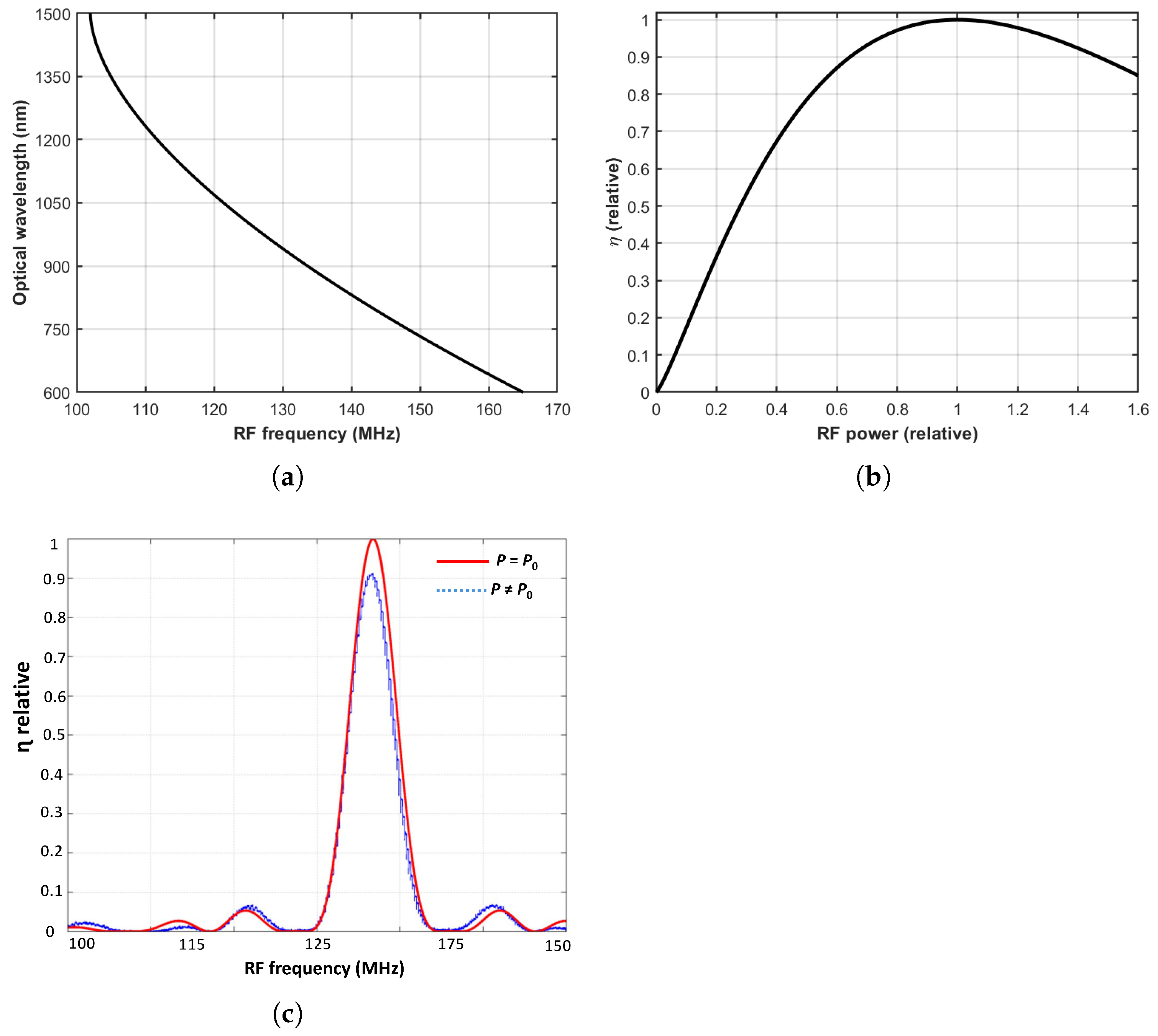
A typical RF frequency versus optical wavelength characteristic for an AOTF crystal is shown in Figure 2a [8]. This figure illustrates that by adjusting the RF signal, a specific optical window can be selected, which contains the desired spectral signature.
Optical instruments in which AOTFs are applied can be categorized into three distinct optical domains: UV, VIS, or UV-based, depending on the material properties of the acousto-optic crystal [14]. Each window corresponds to an approximate one-octave RF bandwidth [8]. This segmentation enables efficient filtering and tuning of optical signals, allowing the AOTF system to manipulate different optical wavelengths.
The diffraction efficiency of an AOTF refers to the percentage of incident light that is diffracted or redirected by the acoustic wave within the crystal [18]. It is a crucial parameter that determines the filter’s performance and its ability to tune and select specific wavelengths of light efficiently. Generally, higher diffraction efficiencies are desirable to ensure that a greater portion of the incident light is effectively filtered and redirected to the desired wavelength. The diffraction efficiency is influenced by the RF power applied to the AOTF [19].
As the RF power increases, the amplitude of the acoustic wave within the crystal also increases. This, in turn, leads to stronger modulation of the refractive index, resulting in a higher diffraction efficiency [18]. However, it is essential to avoid exceeding certain power levels to prevent damage to the crystal. Thus, the objective is to achieve the RF drive level corresponding to the highest AOTF diffraction efficiency, as seen in Figure 2b [8].
The relationship between diffraction efficiency and RF power is not linear, and there is an optimal operating range where the diffraction efficiency is maximized without causing damage to the crystal or distorting the spectral response. This operating range depends on the specific characteristics of the AOTF, including the crystal type and dimensions. Equation (2) gives an approximate formula for the P 0 to its crystal properties given by Equation (2) [8].
P 0 λ 2 H 2 L M
Here, H and L denote the height and length of the transducer, and M denotes the crystal merit figure that depends on the type of material used [20].
Finally, the optical efficiency as a function of both parameters is given by Equation (3) [21]
η = P P 0 sin 2 π 2 P P 0 + Δ Φ π 2 P P 0 + Δ Φ π 2
where P is the power of the acoustic wave in the medium due to the driven RF signal, P 0 is the power required to obtain maximum efficiency given by Equation (2), and Δ Φ is the phase mismatch parameter of the interaction, which is in turn is related by the RF frequency given by Equation (1). This function is also known as the AOTF transmission function.
As shown in Figure 2c [17], the efficiency varies for a fixed optical window as a sinc function of the RF frequency. The red curve corresponds to the condition where the RF drive produces 100% diffraction efficiency, while the blue curve indicates that the crystal is not driven at the correct RF frequency. This reduction in efficiency is governed by the phase mismatch parameter Δ Φ , which appears in the AOTF transmission function of Equation (3) and is itself related to the RF frequency through Equation (1).
The phase mismatch originates from deviations from the Bragg condition. The acoustic wavevector,
K = 2 π f RF v ,
must satisfy the momentum–matching requirement,
k out = k in + K ,
for efficient acousto–optic interaction. This condition defines the Bragg acoustic wavevector K Bragg , corresponding to the RF drive frequency that produces maximum efficiency.
Any deviation from this condition introduces a nonzero phase mismatch given by
Δ Φ = K K Bragg L ,
where L is the acousto–optic interaction length.
When Δ Φ = 0 , the optical and acoustic waves remain phase–synchronous throughout the crystal, allowing the sinc2 transmission function in Equation (3) to reach its maximum, as shown by the red curve. However, when the RF frequency is offset from the Bragg value, K K Bragg . The accumulated phase difference along L causes partial destructive interference among the locally generated diffracted fields. This behaviour produces the lower–amplitude blue curve, indicating that the crystal is not driven at its optimal acoustic frequency and therefore exhibits reduced diffraction efficiency.

2.2. RF Power Amplifier

The design of an RFPA typically begins with choosing its operating class. Conventional RFPAs are designed either according to standard biasing conditions, such as Class-A or Class-AB, or based on specific operating modes, such as Class-E or Class-F [22,23]. Achieving high efficiency in an RFPA requires minimizing power dissipation in the active device, which can be ensured by enforcing the non-overlapping condition expressed in Equation (7):
1 T T V ( ω t ) I ( ω t ) d t = 0
Satisfying this condition allows Class-E and Class-F amplifiers to achieve 100% efficiency theoretically [24]. However, generating the ideal square waveform in Class-F amplifiers necessitates multiple resonators [25], which makes Class-E a more practical choice for many applications.
The development of Class-E RFPAs can be traced back to the late 1940s [26]. By the late 1960s, switched-mode power amplifiers gained popularity due to their inherent non-overlapping operation. This concept was further refined through the introduction of Zero Voltage Switching (ZVS) and Zero Voltage Derivative Switching (ZDS) [27]. In 1975, Sokal et al. [28] formally coined the term Class-E, and Raab later provided the corresponding design equations in 1977 [29].
Two primary load network topologies are commonly employed in Class-E RFPAs: one that neglects the influence of finite DC feed [30] and another that accounts for it [31]. Both designs typically include a series resonator with a high-quality factor ( Q s ) to constrain the fundamental current within the circuit [15,32]. With the advent of modern wireless systems, transmission line-based Class-E topologies were investigated [33,34]. However, in the VHF range, using transmission lines becomes impractical, necessitating the use of discrete lumped components—resistors, inductors, and capacitors—for efficient RFPA implementation.

3. Design Methodology

This section presents the mathematical modeling, design methodology for achieving a wide-bandwidth and selecting an appropriate transistor for Class-E RFPAs. For simplicity, a 50% switching duty cycle is assumed, and the transistor is considered ideal with negligible on-resistance. The ZVS and ZVDS conditions are defined by Equations (8) and (9) [27].
V ( ω t ) | t = 2 π = 0
d V ( ω t ) d ( ω t ) | ω t = 2 π = 0
Based on prior studies, this work focuses on Finite Feed DC Inductance (FDI) Class-E topology [15,35,36].

3.1. Class-E Load Network Topology with Finite DC Feed

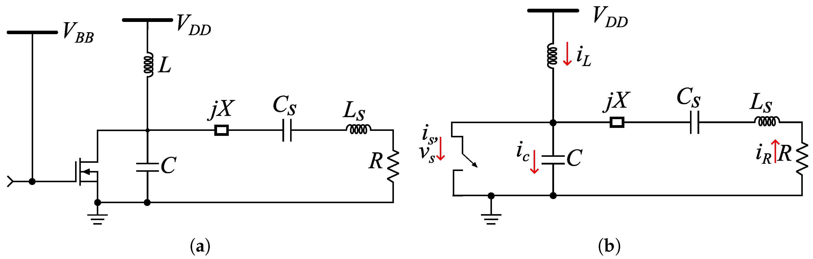
The schematic of a Class-E-tuned switched-mode power amplifier with a finite DC feed is shown in Figure 3a. The load network consists of a feed inductance L, which supplies current to the transistor. The series reactance j X is connected to a series resonant circuit ( L s C s ) that is tuned to the design frequency f o . This configuration is then connected to the optimal load resistance R.
Due to the finite inductance L, the supply current becomes time-varying, denoted as i L ( ω t ) . The equivalent circuit is shown in Figure 3b. The load current is given by Equation (10).
i R ω t = I R sin ω t + ϕ
where ϕ is the initial phase shift and I R is the peak amplitude of the current. For the time interval 0 ω t < π , the switch is on and the current flowing through the switch can be given by Equation (11).
i s ( ω t ) = V D D ω L ω t + I R [ sin ( ω t + ϕ ) sin ( ϕ ) ] 0 ω t π 0 π < ω t 2 π
When the switch is off, in the interval π < ω t 2 π , the current through the switch becomes zero and the current through the capacitor can be given by i c ω t = i L ω t + i R ω t , with Equation (12) the initial condition for the feed inductance L.
i L π = V D D π ω L I R sin ϕ ω L
The switch voltage can be found by solving the differential equation as reported in [35]. The solution is provided by Equation (13).
v s ( ω t ) = 0 0 ω t π V D D [ 1 + C 1 cos ( q ω t ) + C 2 sin ( q ω t ) q 2 p 1 q 2 cos ( ω t + ϕ ) ] π < ω t 2 π
Without loss of generality, and using the initial off-state conditions, Equations (14)–(17), are obtained [35].
C 1 = ( cos q π + q π sin q π ) q p 1 q 2 q cos ϕ cos q ϕ ( 1 2 q 2 ) sin ϕ sin q ϕ
C 1 = ( sin q π q π cos q π ) q p 1 q 2 q cos ϕ cos q ϕ + ( 1 2 q 2 ) sin ϕ sin q ϕ
where, q and p are given by Equations (16) and (17) respectively.
q = 1 ω L C
p = ω L I R V D D
With variable q as a free parameter, the values for the unknown parameters, ϕ , and p can be calculated, applying the ZVS and ZVDS conditions. Two equations with two unknowns can be solved using Equations (18) and (19) to get the required values [35],
C 1 q sin 2 q π + C 2 q cos 2 q π + q 2 p sin ϕ 1 q 2 = 0
C 1 q sin 2 q π q 2 + C 2 q cos 2 q π q 2 + q 2 p cos ϕ 1 q 2 = 0
The parameter q imposes certain limitations due to the extensive design space and the complexity of the governing equations. A detailed study addressing these aspects can be found in [37,38,39]. In particular, the case j X = 0 , corresponding to the parallel class with q = 1.412 [40], is considered here. By solving Equations (18) and (19), the values of p = 1.210 and φ = 15 . 155 ° are obtained. The corresponding component values for R, L, and C are derived as:
R = 1.365 , V D D 2 P o u t
L = 0.732 , R ω
C = 0.685 ω R

3.2. Double Reactance Compensation Technique for Wide Bandwidth

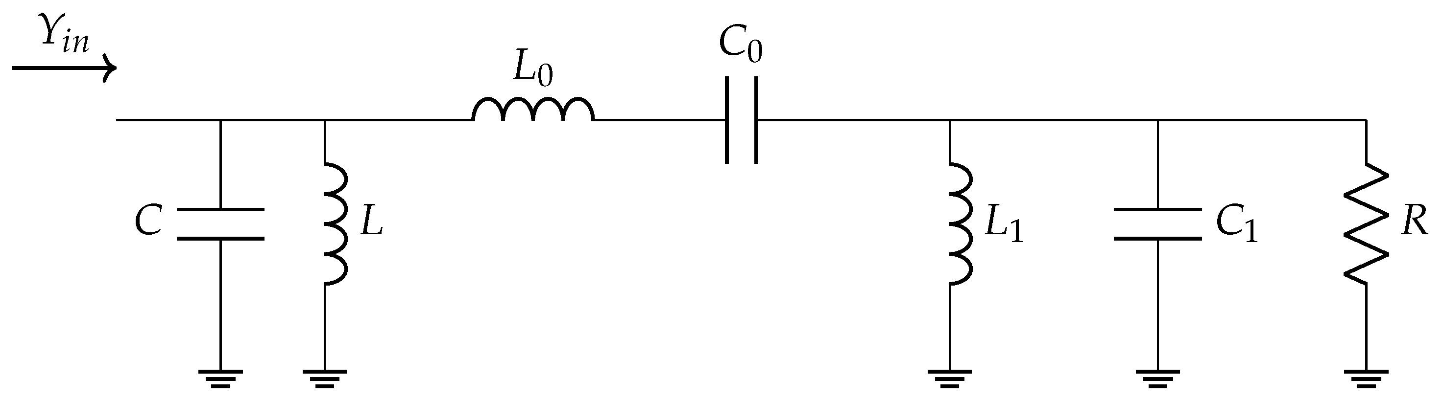
This technique, commonly used to broaden the bandwidth in Class E amplifiers, is known as the reactance compensation technique in standard literature [35,41,42]. The equivalent circuit is shown in Figure 4, and the equivalent admittance for the circuit is given by Equation (23)
Y in = 1 Z in = j ω C + 1 j ω L + 1 1 1 R + j ω C 1 + j ω L 0
where
ω = ω 1 ω 0 2 ω 2 , ω 0 = 1 L 0 C 0
is the resonant frequency.
When considering the reactance compensation principle in a wideband frequency range, the maximized bandwidth can be obtained at ω 0 , and Equation (23) can be expressed as follows:
d Im Y in ( ω ) d ω ω = ω 0 = d 3 Im Y in ( ω ) d ω 3 ω = ω 0 = 0
To obtain the lumped parameters for the proposed double reactance compensation matching network, the input susceptance Im Y in ( ω ) can be expressed as
Im Y in ( ω ) = ω C 1 ω L + ω C 1 R 2 1 ω L 0 C 1 L 0 R 2 1 ω L 0 C 1 2 + ( ω L 0 ) 2
The following condition is then satisfied.
1 ω 0 2 L + C 1 R 2 L 0 R 2 8 ω 0 2 L 0 R 4 C 1 2 + ( C 1 R 2 L 0 ) ( L 0 2 C 1 R 2 ) = 0
From which the lumped parameters are obtained as in Equations (27) and (28)
L 0 = 1.626 R ω 0 , C 0 = 1 ω 0 2 L 0
C 1 = 0.382 L 0 R 2 , L 1 = 1 ω 0 2 C 1
With these closed-form expressions, all the lumped elements required to realize the proposed double reactance compensation network are now fully defined. In the next section, the transistor device is introduced, from which these parameters are incorporated into the complete circuit schematic.

3.3. Transistor Selection

Gallium Nitride (GaN) exhibits superior material properties compared to conventional semiconductors such as silicon. Its high sheet charge density enables large current handling per unit gate periphery, resulting in a high power density and reduced device size [43]. In addition, the elevated saturated drift velocity of GaN supports higher saturation current densities and output power, thereby lowering the capacitance per watt of delivered power.
These attributes—low output capacitance and low drain-to-source resistance per watt—make GaN High Electron Mobility Transistors (HEMTs) highly suitable for switch-mode amplifier applications. In particular, AlGaN/GaN HEMTs provide enhanced performance relative to other technologies, as reviewed in [44,45].
Under radiation-rich space environments, Si-MOS devices face considerable limitations, whereas GaN HEMTs demonstrate strong resilience and have been successfully deployed in multiple space missions [46,47,48,49]. Furthermore, the availability of engineering prototypes and validated nonlinear models enables accurate design and experimental validation.
In this work, the nonlinear large-signal model of the CGH40010 transistor [50] was employed. The device is capable of delivering up to 10 W of output power over a frequency range from DC to 6 GHz, making it well-suited for the AOTF driver, which requires a maximum drive power of 3 W within this bandwidth.

4. Results and Discussion

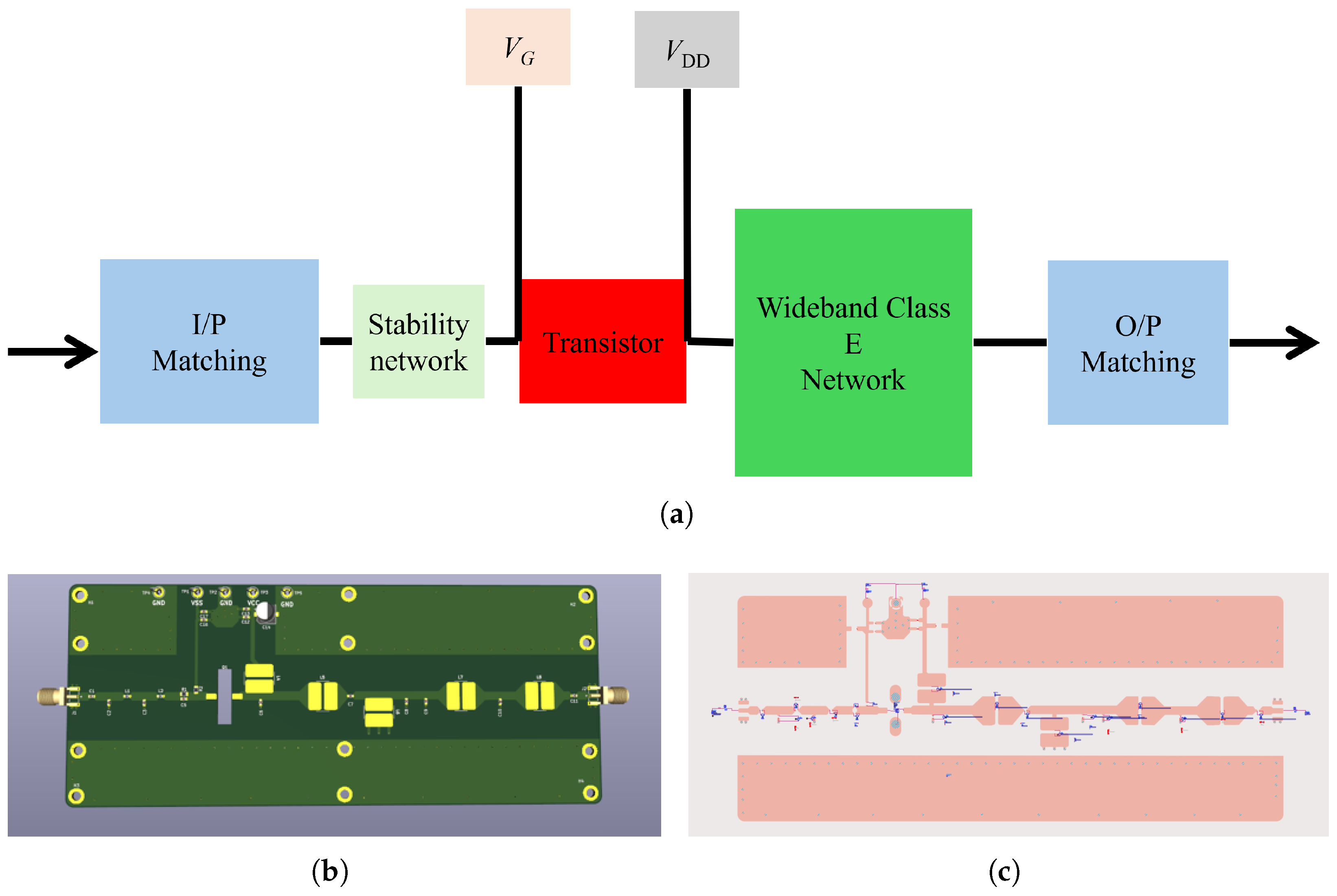
The design of the Class-E parallel circuit with impedance matching is summarized in Figure 5. The block diagram in Figure 5a illustrates the overall circuit architecture, while the corresponding PCB layout is shown in Figure 5b. The PCB was designed on an FR-4 substrate with a thickness of 1.54 mm and a dielectric constant of 4.5, using 50 Ω transmission lines to ensure proper impedance matching. The ADS-based simulation layout, presented in Figure 5c, validates the design methodology and demonstrates the practical feasibility of the proposed circuit.
A parametric optimization strategy is employed to refine the lumped circuit element values, starting from analytically obtained closed-form expressions. During this process, selected lumped components, including inductors and capacitors in the matching and resonant networks, are iteratively varied within predefined fabrication- and tolerance-constrained bounds. A gradient-based optimization algorithm in ADS [51] is used to efficiently update the component values, minimizing deviations from the target performance metrics such as output power, power-added efficiency, and input/output return losses. This approach ensures rapid convergence while accounting for transistor nonlinearities, component tolerances, and layout-induced parasitic effects.
The optimization objectives are defined to achieve the target output power, maximize efficiency, harmonic supression and maintain acceptable input and output return losses, while preserving the Class-E switching conditions. This approach effectively compensates for transistor nonlinearities, component tolerances, substrate losses, and layout-induced parasitic effects that are not fully captured in the ideal analytical model.
Nonlinear large-signal transistor models, together with the vendor-given S2P files of the passive components, are incorporated into the ADS framework, enabling accurate circuit-level and electromagnetic co-simulation and ensuring consistency between analytical predictions, simulated performance, and practical realization.

4.1. RF Considerations

To evaluate performance, ADS simulations were conducted at two different output power levels, 1 W and 3 W, across the frequency range of 100–150 MHz. Nonlinear transistor models were combined with S-parameter files of the passive components (inductors and capacitors) to ensure realistic performance prediction. The design was further optimized to achieve nearly half-octave bandwidth while maintaining high efficiency and effective harmonic suppression.
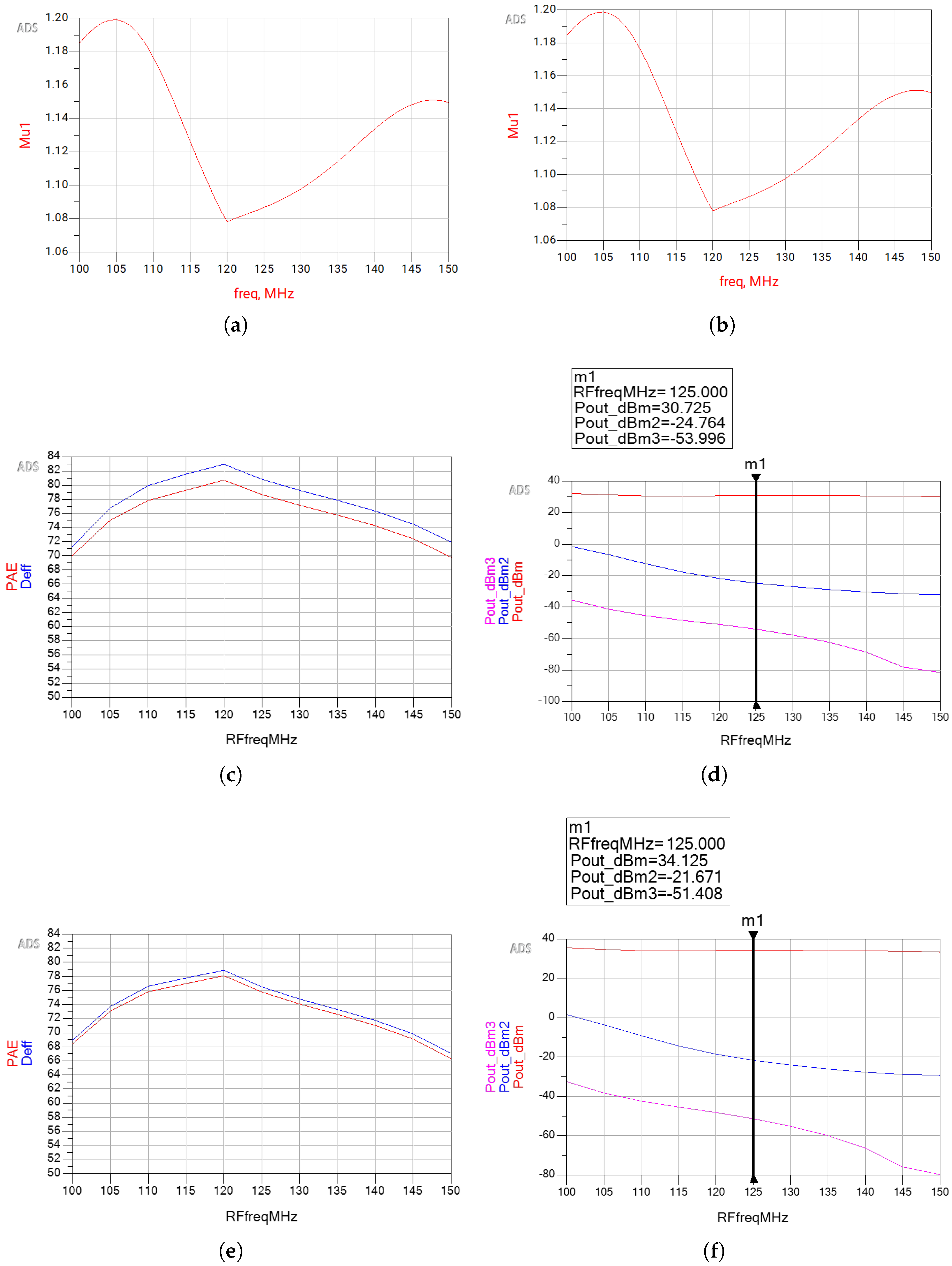
Additionally, stability analysis was performed at both operating points to ensure reliable operation under saturated Class-E conditions. The stability results at the 1 W and 3 W operating points are presented in Figure 6a and Figure 6b, respectively, where the μ -factor remains greater than unity across the entire operating band, confirming unconditional stability. The simulated efficiency and power responses are shown in Figure 6c–f.
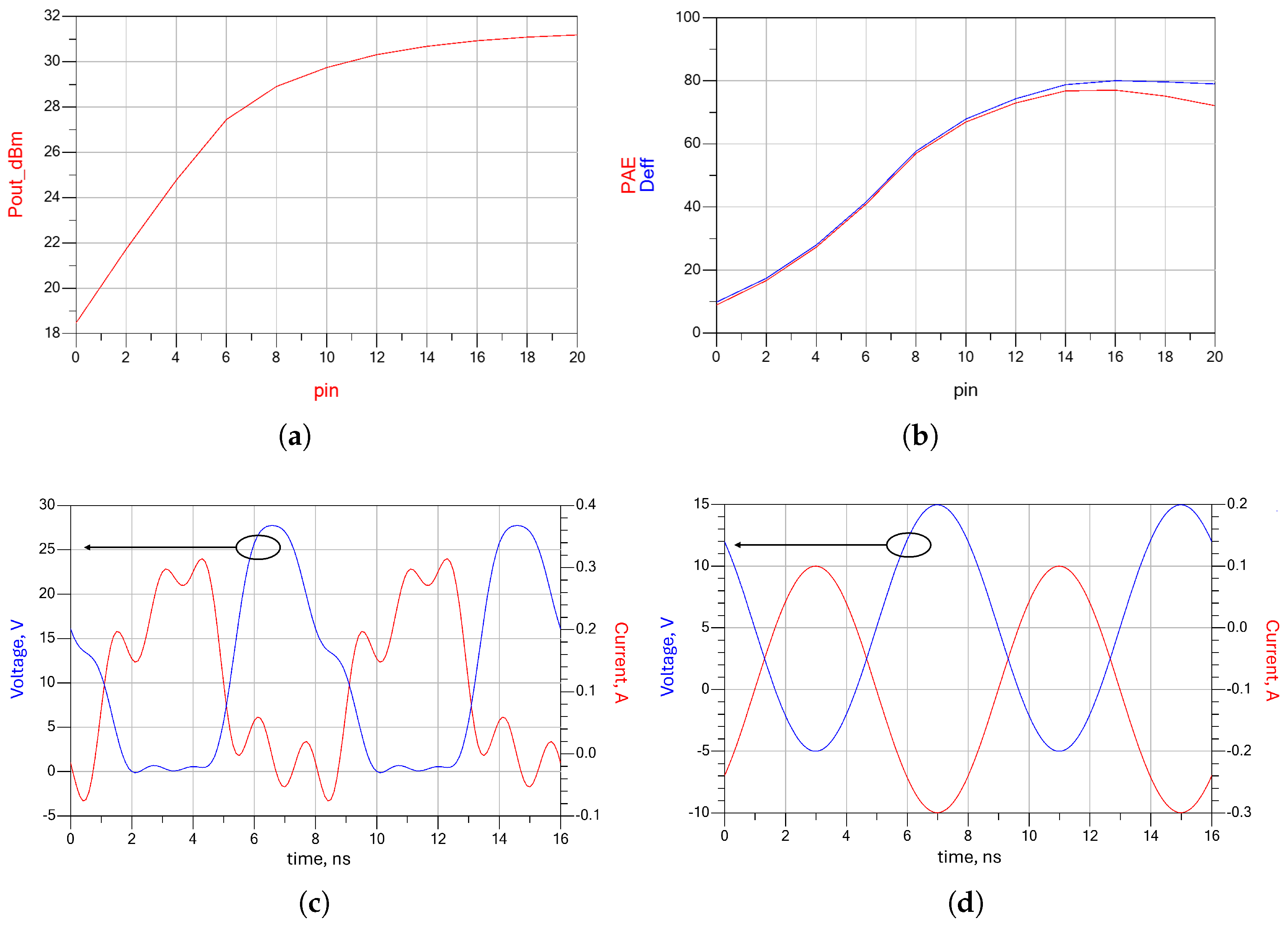
Figure 7 further illustrates the ADS simulation results at 125 MHz. Figure 7a shows the relationship between P i n and P o u t (dBm), while Figure 7b illustrates P i n versus power added efficiency (PAE) and drain efficiency ( D e f f ). The extrinsic voltage and current waveforms at the drain are presented in Figure 7c, and the output current and voltage waveforms are depicted in Figure 7d. Although the amplifier operates in saturation to achieve maximum efficiency, which introduces nonlinearities, the harmonic content at the output remains suppressed below −30 dBc. This is achieved by the second-order low-pass impedance matching network, which effectively combines the Class-E output impedance with the standard 50 Ω load, ensuring proper harmonic suppression and optimal power transfer. Since the output is matched to 50 Ω , the resulting waveform is nearly sinusoidal, making it suitable for driving AOTFs.
At an output power of 1 W, the circuit demonstrates high efficiency across the operating band, as shown in Figure 6c, with the corresponding output power characteristics presented in Figure 6d for a supply voltage of V D D = 10 V. Under this operating condition, the harmonic components remain suppressed below −30 dBc across the entire frequency range. When the output power is increased to 3 W, the efficiency response is shown in Figure 6e, and the corresponding power performance is presented in Figure 6f for V D D = 15 V. Despite the increased voltage and current stress, harmonic suppression is consistently maintained across the band, ranging from approximately −30 dBc for the higher-order harmonics up to −60 dBc for the dominant harmonic components.
As the output power exhibits a non-flat response, a feedback-controlled gain compensation network with tunable output matching has been implemented. This network dynamically adjusts the drive conditions to maintain nearly constant output power, ensuring the AOTF is driven within its optimal range and preserving spectral uniformity and measurement accuracy.
The results confirm the ability of the proposed Class-E parallel circuit to maintain efficient operation while scaling output power by adjusting the supply voltage. The amplifier achieves an efficiency in the range of 65–80% across the operating band, with harmonic levels suppressed below −30 dBc. As discussed in [36], ideal ZVS and ZDS conditions cannot be maintained across the entire broadband frequency range. This limitation leads to a reduction in amplifier efficiency, which is an inherent characteristic of broadband Class-E operation. The double-reactance compensation technique stated in this work can partially mitigate this effect by reducing the efficiency drop, though it cannot fully restore ideal switching conditions.

4.2. Thermal Considerations

Thermal management is a critical design constraint for spaceborne RF amplifiers, where the absence of convective cooling in a vacuum makes conductive heat transfer through the package, PCB, and spacecraft chassis paramount. For the CGH40010 GaN HEMT [50] used in this work, the worst-case power dissipation occurs at the minimum measured power-added efficiency, while the best-case scenario corresponds to the maximum efficiency. At the target 3 W RF output power ( P out ), the dissipated power is calculated as follows for the two cases:
  • Best-case efficiency ( η = 0.80 )
    P diss = P out η P out = 3 0.80 3 0.75 W ,
    T j = T base + P diss · ( R θ JC + R θ CA ) = 70 + 0.75 · ( 2.5 + 5 ) 76   ° C .
  • Worst-case efficiency ( η = 0.65 )
    P diss = P out η P out = 3 0.65 3 1.62 W ,
    T j = T base + P diss · ( R θ JC + R θ CA ) = 70 + 1.62 · ( 2.5 + 5 ) 83   ° C .
Here, T base = 70 °C represents the worst-case spacecraft mounting temperature, R θ JC = 2.5 °C/W is the junction-to-case thermal resistance, and R θ CA 5 °C/W accounts for the PCB and thermal interface material. This analysis shows that, even under worst-case efficiency, the junction temperature remains well below the device’s maximum rated T j , max = 150 °C, confirming the reliability of the selected substrate and conductive heatsinking strategy for spaceborne operation.
These characteristics satisfy the requirements for driving AOTFs. The achieved bandwidth approaches half an octave, indicating that two such amplifiers can be arranged in parallel with an appropriate switching scheme to fully cover a single optical range of the AOTF. Notably, the proposed engineering model can be directly translated into a one-to-one space-qualified implementation, enabling straightforward adaptation for future spaceborne spectroscopic applications.

5. Conclusions and Future Work

In this work, a highly efficient, wideband Class-E parallel circuit with impedance matching was designed, simulated, and analyzed for driving AOTFs in space applications. The PCB was realized on an FR-4 substrate with a thickness of 1.54 mm and a dielectric constant of 4.5, using 50 Ω transmission lines to ensure proper impedance matching. ADS simulations, incorporating nonlinear transistor models and S-parameter files of passive components, demonstrated that the amplifier achieves high efficiency (65–80%) across the 100–150 MHz band while suppressing harmonics below −30 dBc. The results confirm that the proposed design meets the requirements for AOTF operation, with a nearly half-octave bandwidth. Furthermore, the presented engineering model can be directly transformed into a one-to-one space-qualified model, making it suitable for future spaceborne spectroscopic applications.
For future work, experimental validation through PCB fabrication and measurements is planned to compare results with simulations, with particular focus on efficiency, harmonic suppression, and thermal performance. Integration with AOTF systems will enable evaluation of real-world performance under operational conditions. Finally, development of a fully space-qualified version, including radiation-hardening and thermal management, is envisioned to facilitate deployment in spaceborne spectroscopic applications.

Author Contributions

Conceptualization, P.K.G. and J.V.; Methodology, P.K.G.; Validation, P.K.G.; Formal analysis, P.K.G.; Investigation, P.K.G.; Resources, P.K.G.; Writing—original draft, P.K.G.; Writing—review and editing, J.V.; Visualization, P.K.G.; Supervision, J.V. and J.L.; Project administration, J.L.; Funding acquisition, J.V. All authors have read and agreed to the published version of the manuscript.

Funding

This research is supported by Delft University of Technology, Netherlands.

Institutional Review Board Statement

Not applicable. This study did not involve human participants or animals, and therefore, ethical approval was not required.

Informed Consent Statement

Not applicable. This study did not involve human participants.

Data Availability Statement

The data presented in this study are available from the corresponding author upon reasonable request. The data are not publicly available due to intellectual property considerations and ongoing research activities related to space-qualified RF system development.

Acknowledgments

The authors thank the editor of the journal and the anonymous reviewers for their valuable suggestions regarding this paper.

Conflicts of Interest

The authors declare no conflicts of interest. The funders had no role in the design of the study; in the collection, analyses, or interpretation of data; in the writing of the manuscript; or in the decision to publish the results.

Abbreviations

The following abbreviations are used in this manuscript:
AOTFAcousto-Optical Tunable Filters
DEDrain Efficiency
P out Fundamental Output Power
P out 2 First Harmonic Output Power
P out 3 Second Harmonic Output Power
P diss Power Dissipated
HFHigh Frequency
HBHarmonic Balance
MFMedium Frequency
MRIMagnetic Resonance Imaging
PAEPower Added Efficiency
RFPARadio Frequency Power Amplifier
VHFVery High Frequency
ZVDSZero Voltage Derivative Switching
ZVSZero Voltage Switching

References

  1. Vanhamel, J.; Berkenbosch, S.; Dekemper, E.; Leroux, P.; Neefs, E.; Lil, E.V. Practical Driving Electronics for an AOTF-Based NO2 Camera. IEEE Trans. Instrum. Meas. 2019, 68, 874–881. [Google Scholar] [CrossRef]
  2. Korablev, O.; Fedorova, A.; Villard, E.; Joly, L.; Kiselev, A.; Belyaev, D.; Bertaux, J.L. Characterization of the stray light in a space borne atmospheric AOTF spectrometer. Opt. Express 2013, 21, 18354. [Google Scholar] [CrossRef] [PubMed]
  3. Harris, S.E.; Wallace, R.W. Acousto-Optic Tunable Filter. J. Opt. Soc. Am. 1969, 59, 744–747. [Google Scholar] [CrossRef]
  4. Pang, Y.; Zhang, K.; Lang, L. Review of acousto-optic spectral systems and applications. Front. Phys. 2022, 10, 1102996. [Google Scholar] [CrossRef]
  5. FiberOptics4Sale.com. Acousto-Optic Devices and Applications. Available online: https://www.fiberoptics4sale.com/blogs/wave-optics/acousto-optic-devices-and-applications (accessed on 20 January 2026).
  6. European Space Agency. Altius: ESA’s Ozone Mission. Launch Date Listed on Page: 2027. Available online: https://www.esa.int/Applications/Observing_the_Earth/Altius (accessed on 2 October 2025).
  7. Georgiev, G.; Glenar, D.A.; Hillman, J.J. Spectral characterization of acousto-optic filters used in imaging spectroscopy. Appl. Opt. 2002, 41, 209–217. [Google Scholar] [CrossRef]
  8. Brimrose Corporation. Free Space Acousto-Optic Tunable Filters. Available online: https://www.brimrose.com/free-space-ao/acousto-optic-tunable-filters (accessed on 31 December 2025).
  9. Evident Scientific. Acousto-Optic Tunable Filters (AOTFs)—Confocal Microscopy Introduction. Available online: https://evidentscientific.com/en/microscope-resource/knowledge-hub/techniques/confocal/aotfintro (accessed on 31 December 2025).
  10. Gupta, N.; Voloshinov, V. Hyperspectral imaging performance of a TeO2 acousto-optic tunable filter in the ultraviolet region. Opt. Lett. 2005, 30, 985–987. [Google Scholar] [CrossRef]
  11. Korablev, O.I.; Belyaev, D.A.; Dobrolenskiy, Y.S.; Trokhimovskiy, A.Y.; Kalinnikov, Y.K. Acousto-optic tunable filter spectrometers in space missions [Invited]. Appl. Opt. 2018, 57, C103. [Google Scholar] [CrossRef]
  12. Korablev, O.; Trokhimovsky, A.Y.; Kalinnikov, Y.K. AOTF spectrometers in space missions and their imaging capabilities. SPIE Proc. 2017, 10562, 283. [Google Scholar] [CrossRef]
  13. Vanhamel, J. An Overview of Analog and Digital RF Generator Techniques, Suitable for Space-Based AOTF Applications. Appl. Sci. 2025, 15, 8739. [Google Scholar] [CrossRef]
  14. Dekemper, E.; Fussen, D.; Pieroux, D.; Vanhamel, J.; Van Opstal, B.; Vanhellemont, F.; Mateshvili, N.; Franssens, G.; Voloshinov, V.; Janssen, C.; et al. ALTIUS: A spaceborne AOTF-based UV-VIS-NIR hyperspectral imager for atmospheric remote sensing. SPIE Proc. 2014, 9241, 92410L. [Google Scholar] [CrossRef]
  15. Gogoi, P.K.; Sharma, A.; Vanhamel, J.; Loicq, J. Investigating the Bounds of Quality Factor for Class-E Series-Tuned RF Power Amplifiers and Their Computer-Aided Optimization. Appl. Sci. 2024, 14, 11881. [Google Scholar] [CrossRef]
  16. Vanhamel, J.; Dekemper, E.; Berkenbosch, S.; Clairquin, R. Novel acousto-optical tunable filter (AOTF) based spectropolarimeter for the characterization of auroral emission. Instrum. Sci. Technol. 2021, 49, 245–257. [Google Scholar] [CrossRef]
  17. Dupont, S.; Kastelik, J.C.; VanHamel, J. Design and testing of a multi-electrode apodized acousto-optic filter for arbitrary polarized light. Appl. Opt. 2024, 63, 2487–2493. [Google Scholar] [CrossRef]
  18. Goutzoulis, A.P. Design and Fabrication of Acousto-Optic Devices; CRC Press: Boca Raton, FL, USA, 2021. [Google Scholar] [CrossRef]
  19. Dekemper, E.; Vanhamel, J.; Opstal, B.V.; Fussen, D.; Voloshinov, V.B. Influence of driving power on the performance of UV KDP-based acousto-optical tunable filters. J. Opt. 2015, 17, 075404. [Google Scholar] [CrossRef]
  20. Vanhamel, J.; Dekemper, E.; Voloshinov, V.B.; Neefs, E.; Fussen, D. Electrical bandwidth testing of an AOTF transducer as a function of the optical diffraction efficiency. J. Opt. Soc. Am. A 2019, 36, 1361. [Google Scholar] [CrossRef]
  21. Chang, I.C. Acousto-optic devices and applications. In Handbook of Optics; McGraw-Hill: New York, NY, USA, 1995; Volume 2, pp. 1–54. [Google Scholar]
  22. Colantonio, P.; Giannini, F.; Limiti, E. High Efficiency RF and Microwave Solid State Power Amplifiers; John Wiley & Sons: Hoboken, NJ, USA, 2009; p. 498. [Google Scholar]
  23. Gogoi, P.K.; Vanhamel, J.; Gill, E.; Loicq, J. Alternative Categorization of Radio Frequency Power Amplifier for Generalized Design Insights. Designs 2025, 9, 83. [Google Scholar] [CrossRef]
  24. Cripps, S. RF power amplifiers for wireless communications. IEEE Microw. Mag. 2000, 1, 64. [Google Scholar] [CrossRef]
  25. Cripps, S.C. Advanced Techniques in RF Power Amplifier Design; Artech House: Boston, MA, USA; London, UK, 2002. [Google Scholar]
  26. Grebennikov, A.; Raab, F.H. A history of switching-mode Class-E techniques: The development of switching-mode Class-E techniques for high-efficiency power amplification. IEEE Microw. Mag. 2018, 19, 26–41. [Google Scholar] [CrossRef]
  27. Eroglu, A. RF Circuit Design Techniques for MF-UHF Applications; CRC Press: Boca Raton, FL, USA, 2017. [Google Scholar]
  28. Sokal, N.; Sokal, A. Class E—A new class of high-efficiency tuned single-ended switching power amplifiers. IEEE J. -Solid-State Circuits 1975, 10, 168–176. [Google Scholar] [CrossRef]
  29. Raab, F. Idealized operation of the class E tuned power amplifier. IEEE Trans. Circuits Syst. 1977, 24, 725–735. [Google Scholar] [CrossRef]
  30. Raab, F.H. Effects of circuit variations on the class E tuned power amplifier. IEEE J.-Solid-State Circuits 1978, 13, 239–247. [Google Scholar] [CrossRef]
  31. Smith, G.; Zulinski, R. An exact analysis of class E amplifiers with finite DC-feed inductance at any output Q. IEEE Trans. Circuits Syst. 1990, 37, 530–534. [Google Scholar] [CrossRef]
  32. Grebennikov, A.; Jaeger, H. Class E with parallel circuit—A new challenge for high-efficiency RF and microwave power amplifiers. In Proceedings of the 2002 IEEE MTT-S International Microwave Symposium Digest (Cat. No.02CH37278), Seattle, WA, USA, 2–7 June 2002; Volume 3, pp. 1627–1630. [Google Scholar] [CrossRef]
  33. Mader, T.; Popovic, Z. The transmission-line high-efficiency class-E amplifier. IEEE Microw. Guid. Wave Lett. 1995, 5, 290–292. [Google Scholar] [CrossRef]
  34. Wilkinson, A.; Everard, J. Transmission-line load-network topology for Class-E power amplifiers. IEEE Trans. Microw. Theory Tech. 2001, 49, 1202–1210. [Google Scholar] [CrossRef]
  35. Grebennikov, A.; Franco, M.J. Switchmode RF and Microwave Power Amplifiers; Academic Press: Cambridge, MA, USA, 2012. [Google Scholar]
  36. Gogoi, P.K.; Ştefănescu, Ş.; Vanhamel, J.; Loicq, J. An Open-Source graphical tool for class E PA design exploration and optimization. Results Eng. 2026, 29, 108472. [Google Scholar] [CrossRef]
  37. Casallas, I.; Paez-Rueda, C.I.; Perilla, G.; Pérez, M.; Fajardo, A. Design methodology of the Class-E power amplifier with finite feed inductance—A tutorial approach. Appl. Sci. 2020, 10, 8765. [Google Scholar] [CrossRef]
  38. Acar, M.; Annema, A.J.; Nauta, B. Analytical design equations for Class-E power amplifiers. IEEE Trans. Circuits Syst. I Regul. Pap. 2007, 54, 2706–2717. [Google Scholar] [CrossRef]
  39. Kr Gogoi, P.; Ştefănescu, Ş.; Sharma, A. Comments on “Analytical Design Equations for Class-E Power Amplifier”. IEEE Trans. Circuits Syst. I Regul. Pap. 2025, 72, 5297–5298. [Google Scholar] [CrossRef]
  40. Grebennikov, A. Simple design equations for broadband Class-E power amplifiers with reactance compensation. In Proceedings of the 2001 IEEE MTT-S International Microwave Sympsoium Digest (Cat. No.01CH37157), Phoenix, AZ, USA, 20–24 May 2001; Volume 3, pp. 2143–2146. [Google Scholar] [CrossRef]
  41. Gelsthorpe, R.; Aitchison, C. Analytical evaluation of the components necessary for double reactance compensation of an oscillator. Electron. Lett. 1976, 12, 485–486. [Google Scholar] [CrossRef]
  42. Zhao, Z.; Zhu, X. Broadband Class-E Power Amplifier Design Employing a Double Reactance Compensation Matching Network. In Proceedings of the 2022 Asia-Pacific Microwave Conference (APMC), Yokohama, Japan, 29 November–2 December 2022; pp. 689–691. [Google Scholar] [CrossRef]
  43. Satoh, T.; Osawa, K.; Nitta, A. GaN HEMT for Space Applications. In Proceedings of the 2018 IEEE BiCMOS and Compound Semiconductor Integrated Circuits and Technology Symposium (BCICTS), San Diego, CA, USA, 15–17 October 2018; pp. 136–139. [Google Scholar] [CrossRef]
  44. Pengelly, R.S.; Wood, S.M.; Milligan, J.W.; Sheppard, S.T.; Pribble, W.L. A review of GaN on SiC high electron-mobility power transistors and MMICs. IEEE Trans. Microw. Theory Tech. 2012, 60, 1764–1783. [Google Scholar] [CrossRef]
  45. Husna Hamza, K.; Nirmal, D. A review of GaN HEMT broadband power amplifiers. AEU Int. J. Electron. Commun. 2020, 116, 153040. [Google Scholar] [CrossRef]
  46. Boomer, K.; Scheick, L. Body of Knowledge for Gallium Nitride Power Electronics; National Aeronautics and Space Administration: Washington, DC, USA, 2020. Available online: https://ntrs.nasa.gov/api/citations/20205007412/downloads/GaN%20BOK.pdf (accessed on 1 December 2025).
  47. Shenoy, T.; Johnson, R.; Tanabe, J.; Beauchamp, R.; Yam, L.; Gim, Y.; Heyer, D.; Plaut, J. A GaN HF-band Power Amplifier using Class-D Topology for Jupiter Ice Penetrating Radar. In Proceedings of the IEEE MTT-S International Microwave Symposium Digest, Denver, CO, USA, 19–24 June 2022; Volume 2022, pp. 214–217. [Google Scholar] [CrossRef]
  48. Raab, F.H. GaN-FET Class-E Amplifier for 60-MHz Radar. In Proceedings of the 2020 50th European Microwave Conference (EuMC), Utrecht, The Netherlands, 12–14 January 2021; pp. 1099–1102. [Google Scholar] [CrossRef]
  49. Öncü, E.; Tutgun, R.; Aktas, E. On the design considerations of solid-state power amplifiers for satellite communications: A systems perspective. Int. J. Satell. Commun. Netw. 2023, 41, 589–598. [Google Scholar] [CrossRef]
  50. MACOM. CGH40010 10 W, DC-6 GHz, RF Power GaN HEMT. Available online: https://cdn.macom.com/datasheets/CGH40010.pdf (accessed on 20 January 2026).
  51. Keysight Technologies. Advanced Design System 2017: Electromagnetic Simulation; Keysight Technologies Incorporated: Santa Rosa, CA, USA, 2017; Available online: https://edadownload.software.keysight.com/eedl/ads/2017/pdf/Electromagnetic.pdf (accessed on 20 January 2026).
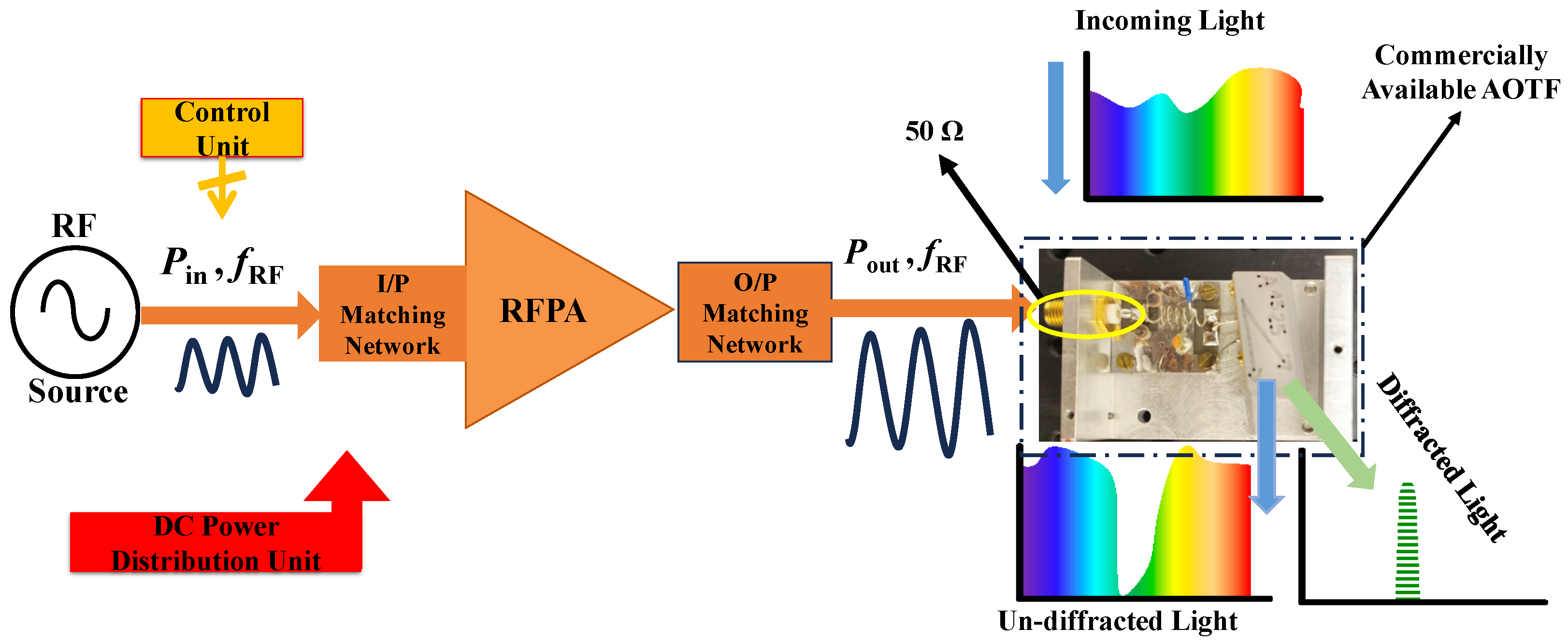
Figure 1. Basic driving principle of AOTFs with its associated electronics.
Applsci 16 01646 g001
Figure 2. Illustrations of various parameters of a typical AOTF: (a) RF drive frequency vs. optical wavelength, (b) RF power vs. relative diffraction efficiency, and (c) Diffraction efficiency vs. RF parameters for a fixed optical wavelength [17].
Applsci 16 01646 g002
Figure 3. Class-E with finite DC feed: (a) schematic diagram and (b) equivalent circuit representation with the arrows showing the instantaneous current direction.
Applsci 16 01646 g003
Figure 4. Equivalent circuit of the double reactance compensation matching network.
Applsci 16 01646 g004
Figure 5. Final Class-E parallel circuit with impedance matching: (a) block diagram, (b) PCB layout, and (c) ADS simulation window.
Applsci 16 01646 g005
Figure 6. ADS simulation results of the wideband Class-E parallel power amplifier with impedance matching: (a) stability analysis at 1 W output power, (b) stability analysis at 3 W output power, (c) efficiency (PAE and DE) at approximately 1 W output, (d) output power at approximately 1 W ( P out , fundamental and harmonics) with V D D = 10 V, (e) efficiency at approximately 3 W output, and (f) output power at approximately 3 W with V D D = 18 V. (PAE: power-added efficiency; DE: drain efficiency; P out : fundamental power; P out 2 : first harmonic; P out 3 : second harmonic).
Applsci 16 01646 g006
Figure 7. ADS simulation results at 125 MHz at 1 Watt output power (a) P i n vs. P o u t (dBm) and (b) P i n vs. PAE and Deff (c) extrinsic voltage and current waveform at drain (d) output current and voltage waveforms.
Applsci 16 01646 g007
Disclaimer/Publisher’s Note: The statements, opinions and data contained in all publications are solely those of the individual author(s) and contributor(s) and not of MDPI and/or the editor(s). MDPI and/or the editor(s) disclaim responsibility for any injury to people or property resulting from any ideas, methods, instructions or products referred to in the content.