1. Introduction
In recent times, the aviation industry has been facing mounting pressure to reduce its environmental footprint and fossil fuel dependency amid growing climate change concerns. Electric aircraft have emerged as a promising solution, offering zero-emission flights, reduced noise pollution, and lower maintenance costs [
1,
2,
3,
4,
5]. With increasing renewable energy adoption, these aircraft could potentially operate with minimal carbon impact. However, several significant challenges impede the widespread adoption of electric aircraft. Current power systems have substantially lower power density compared to jet fuel, limiting range and payload capacity. The weight of batteries and electric propulsion systems significantly impacts aircraft performance, while the need for charging infrastructure presents additional logistical hurdles [
6,
7]. Thermal management in high-power electric systems also remains a critical safety and efficiency concern [
8]. Superconducting power systems offer a potential breakthrough by utilizing materials with zero electrical resistance at cryogenic temperatures. These systems provide multiple advantages over traditional technology, including increases in power density, power capacity, and volumetric density [
9,
10,
11,
12]. These benefits directly address many limitations of conventional electric propulsion systems. The implementation of high-temperature superconducting (HTS) devices for aircraft applications includes motors, generators, and cables. For aircraft applications, HTS DC cables are envisioned as part of the distribution systems to enable optimization of the motors and generator. When developing DC HTS cables, it is important to understand how the load profiles, as well as cryogenic operating conditions, can influence the design of the electrical insulation [
13].
Under DC stress, the electric field distribution exhibits complex time- and temperature-dependent behavior, distinctly different from AC systems [
14]. This behavior is characterized by a transition from capacitive distribution to resistive distribution, influenced by material properties such as permittivity and electrical conductivity, and governed by dielectric polarization phenomena [
15]. The temperature dependency of DC electric fields becomes particularly critical in cryogenic environments where material properties significantly deviate from room-temperature behavior. The charging and discharging time constants, crucial for proper insulation design, may be substantially altered at these extremely low temperatures. Despite extensive research on DC insulation systems, there remains a significant knowledge gap regarding their behavior under aviation-specific load profiles at cryogenic temperatures.
In aviation applications, DC power systems face distinctive operational patterns, unlike terrestrial power grids. While conventional grid cables maintain continuous energization, aircraft power systems experience frequent energization/de-energization cycling aligned with flight durations, typically less than 5 h [
16]. Between flights, there is a turnaround time of 1–2 h, which may not be sufficient to achieve complete discharge in the electrical insulation, creating unique stress patterns on the insulation system. This cyclic operation at cryogenic temperatures introduces unprecedented challenges in understanding charge accumulation, space charge behavior, and dielectric response [
17].
Understanding the performance of electrical insulation under transient conditions is essential for developing reliable insulation systems for future electric aircraft. This study aims to investigate the time-dependent transient DC electric field distribution of HTS cable insulation at cryogenic temperature under aviation-typical duty cycles, providing crucial insights for the design of robust HTS cable systems for aircraft applications. By understanding these impacts, we can develop more resilient insulation systems of HTS power devices for aircraft applications.
1.1. Insulation Design Concepts of HTS Cable for Aviation Applications
The DC power system of an electric aircraft resembles an “isolated microgrid”, where the consumption, generation, and storage components are connected through power distribution cables. The total power demand of an electric aircraft can range from 10 to 40 MW based on the passenger capacity and aircraft class. The current of an HTS cable is a function of the number of HTS tapes connected in parallel with one another, with typical HTS cable current ratings being between 1 and 5 kA. Based on the current ratings, the expected operating voltage for an HTS cable for aircraft application would be in the range of ±0.5–5 kV DC [
18]. Due to its extended operating temperature range and reduced risk of asphyxiation, helium gas (GHe) is the preferred cryogen for aviation applications [
12]. However, the drawback with GHe is its low dielectric breakdown strength (8 kV
rms/mm in a uniform electric field at 77 K and 2.0 Mpa) [
12].
HTS cables are installed inside a cryostat, which provides a thermally isolated cryogenic environment. The weight and dimensions of the cryostat should be optimal to achieve high power density. Inner diameters of commercially available cryostats are in the range of 30–60 mm. To reduce the burden on the cryogenic infrastructure and ensure high overall power density, it is preferable to have multiple HTS cables installed within a single cryostat. In this regard, an HTS cable with a conductor diameter of 0.25 inch (6.35 mm) and an insulation thickness of 3 mm was considered [
12]. An HTS conductor with these dimensions is capable of operating at the desired current levels seen for electric aircraft applications.
As multiple HTS cables are installed within a single cryostat, it necessitates that the electrical insulation for the HTS cables is also at cryogenic temperature. Conventional insulation materials become cracked and brittle at cryogenic temperatures, and techniques have been developed to ensure mechanical and material compatibility [
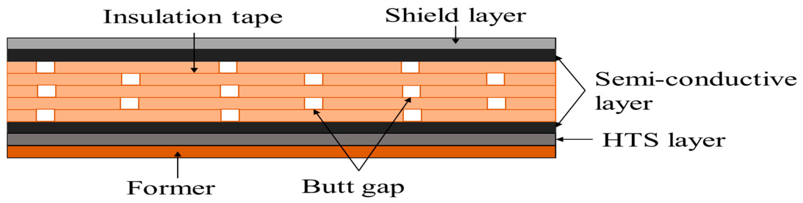
19]. In this regard, the insulation system for HTS is designed in a lapped tape configuration to mitigate the generation of mechanical stresses due to a mismatch in the coefficient of thermal expansion between the conductor and insulation layer. In a lapped tape insulation system, insulation tape is helically wrapped with butt gaps introduced to allow for mechanical flexibility of the cable [
12]. A schematic of lapped tape insulation is shown in
Figure 1. This lapped tape insulation system for a GHe-cooled HTS cable is a composite insulation system where the butt gaps are filled with the cryogen, and for aviation applications, this can be assumed to be GHe. Due to the permittivity mismatch between GHe and the insulation system, the butt gap regions are susceptible to electric field enhancement. Also, the interfacial regions of the HTS cable, which include the conductor and insulation layer as well as the insulation and ground layer, are additional locations of electric field enhancement, as there are voids within this region due to a non-adhesive lapped tape being utilized for the electrical insulation. Hence, while the lapped tape insulation design addresses the mechanical stresses at cryogenic temperatures, it makes the GHe-cooled HTS cable susceptible to partial discharge activity. Partial discharge (PD) is a localized breakdown in an insulation system [
20]. Long-term partial discharge activity can degrade any insulation system, which in turn results in insulation failure of the HTS cable [
21]. Any insulation failure in the HTS cable can be a serious threat to aircraft operation. Hence, the efficient design and materials for electrical insulation systems for a GHe-cooled HTS cable are important factors for the reliable operation of an electric aircraft.
Normally, polypropylene-laminated paper (PPLP) is used as a material for HTS cable insulation due to its excellent cryogenic performance. The advantage of PPLP is that it yields low permittivity (ε
r = 2.3), which is very suitable as an insulating material. However, due to its porous nature, PPLP yields a risk of moisture ingression during manufacturing and maintenance [
12]. Moisture ingression can cause ice formation, which degrades insulation conditions. Considering this, the feasibility of alternative materials needs to be investigated for HTS cable insulation. In [
12], polyamide (Kapton) is used as HTS cable insulation due to its excellent moisture ingression resistance, mechanical, and thermal properties at cryogenic temperatures. In this paper, Kapton (ε
r = 3.5), Polyethene (PE, ε
r = 2.3), and Polytetrafluoroethylene (PTFE, ε
r = 2.1) have been chosen as insulating materials for the simulation study.
1.2. Theoretical Concept of Electric Field Distribution Under DC Stress
For efficient insulation design of any DC power device, it is important to have proper knowledge about the electric field (e-field) distribution of the insulation system under DC stress. In this regard, it is important to note here that under DC stress, the electric field distribution is time- and temperature-dependent, and it is quite different from the AC field distribution.
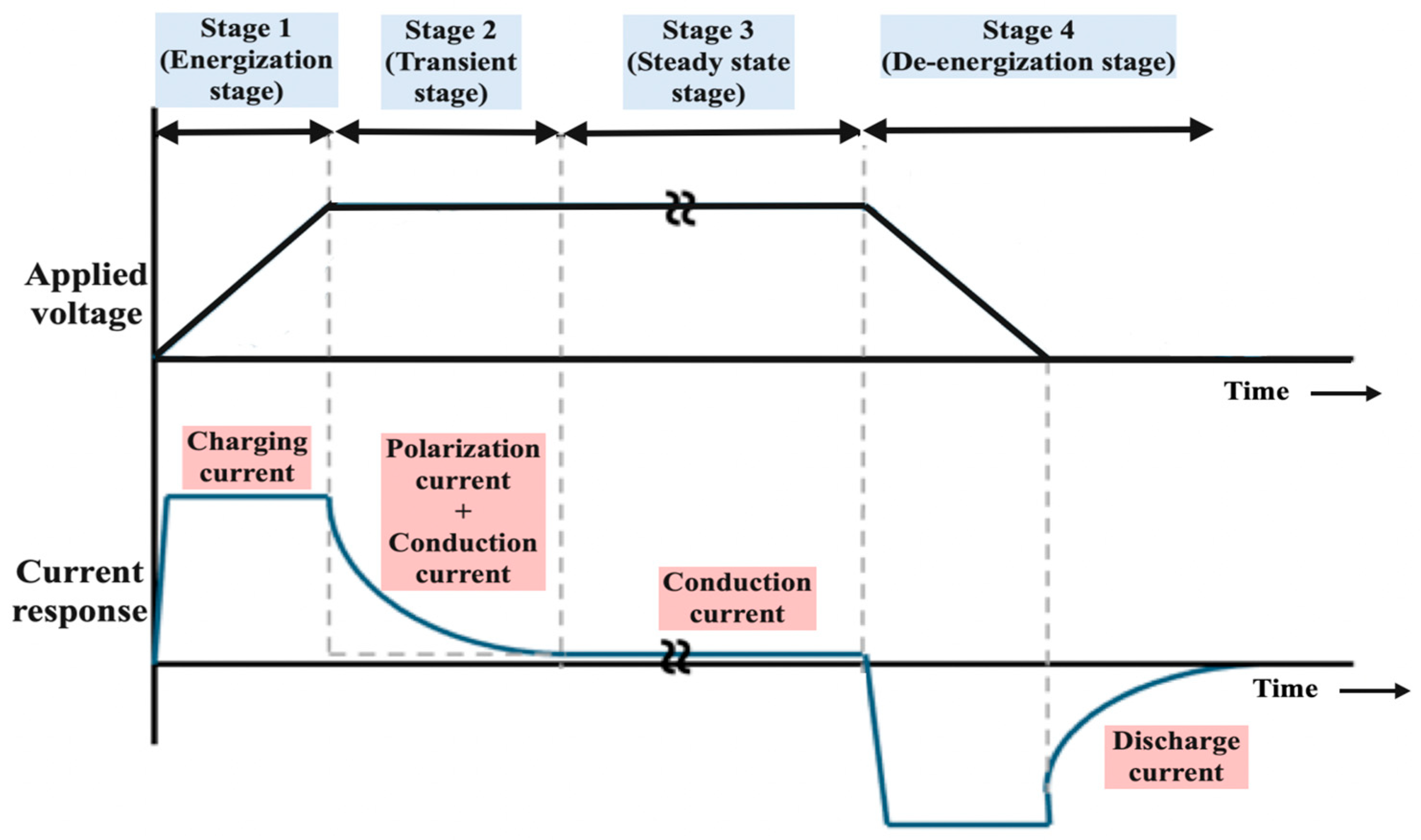
The e-field distribution of an insulation system under DC stress can be represented by different stages from energization to de-energization (shown in
Figure 2) [
14]. The first stage indicates the energization process of the DC supply. In this stage, only displacement current/charging current flows. Hence, the electric field distribution of the insulation system is purely capacitive and completely driven by the permittivity of the material. The mathematical equation to calculate the capacitive field is given in Equation (1):
The second stage indicates the transition of the electric field distribution from capacitive to resistive. In this stage, the electric field distribution transitions from a permittivity-driven distribution to an electrical conductivity-driven distribution. The e-field distribution of the insulation system at stage 2 is driven by both the permittivity and electrical conductivity of the insulating material. The governing equation in this stage is given as
In Equations (2) and (3),
J, and
Q indicate vacuum permittivity, insulating material permittivity, electrical conductivity, current density, and accumulated charge, respectively. The time constant (
) for the electric field transition process is given as [
22]
Once the transient process is over, only conduction current/resistive current flows through the insulation, which is indicated by stage 3. In stage 3, the e-field distribution is purely resistive. The electric field distribution in stage 3 is completely driven by the electrical conductivity of the material [
23]. In stage 4, the DC supply is de-energized, and depolarization current or discharge current flows through the insulation. During this, the e-field distribution is dependent on the accumulated charge density. This e-field disappears with the same time constant as given in Equation (2) [
14].
1.3. Electrical Conductivity Measurement at Cryogenic Temperature
It is well known that the e-field distribution under DC stress is dependent on the permittivity and electrical conductivity of the material. According to [
23], the electrical conductivity of a material is a temperature-dependent function. Hence, based on Equation (2), it can be said that the time constant of the electric field transition is also dependent on operating temperature. Therefore, it can be said that the electrical conductivity data at the intended operating temperature enable accurate modeling of the e-field distribution to enable reliable and energy-efficient designs. However, there is limited electrical conductivity data at cryogenic temperatures in helium gas. Considering this, an electrical conductivity measurement setup was fabricated in the laboratory in accordance with the ASTM D257 standard [
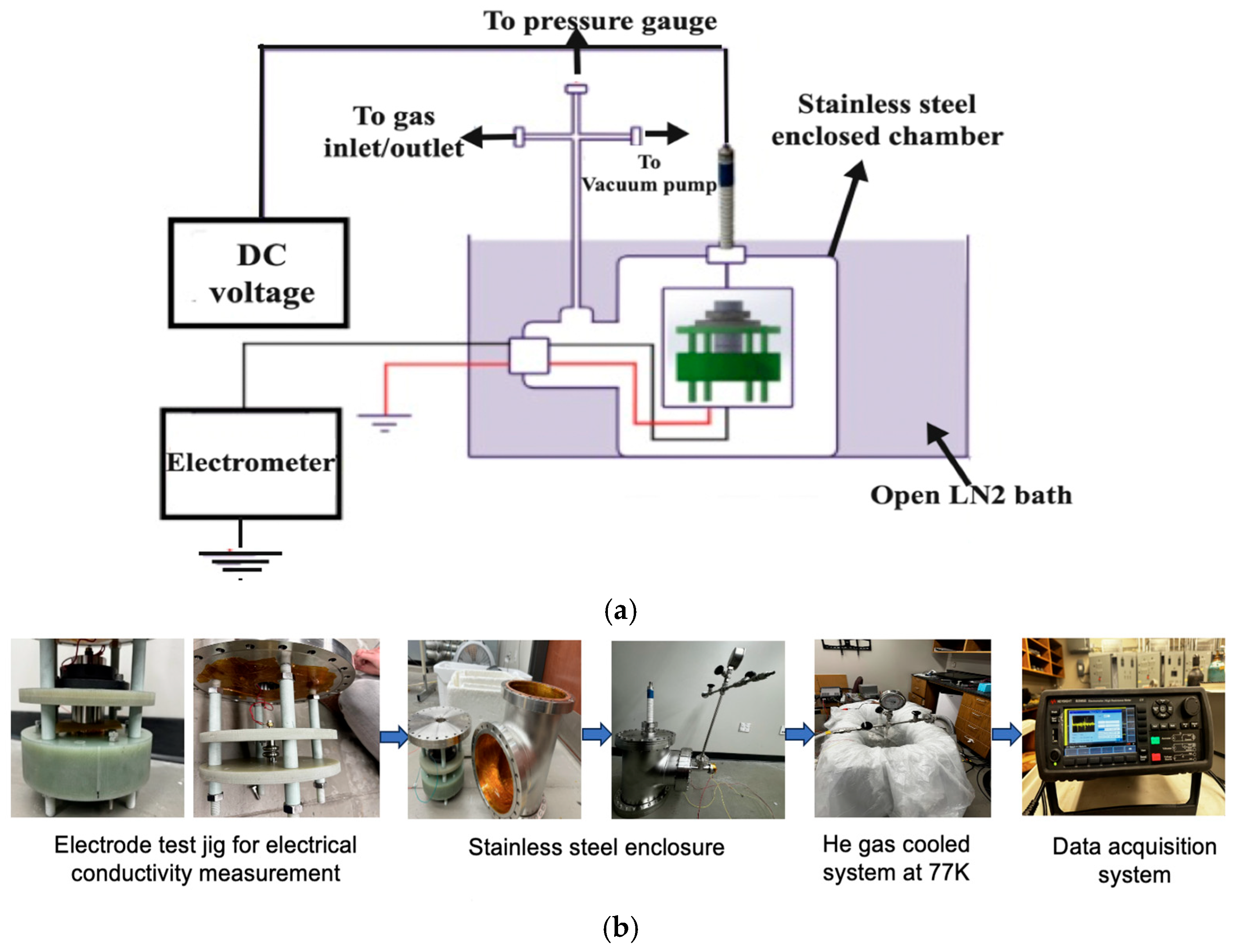
24]. This setup can measure the electrical conductivity of any insulating material (a pressurized GHe environment) and gaseous medium (GHe) at 77 K temperature.
Figure 3a,b show the schematic diagram and photograph of the electrical conductivity measurement setup in a gaseous helium environment at 77 K temperature. This setup consists of a cryogenically compatible electrode test jig, which was placed in a gaseous helium-filled stainless-steel enclosure. For the electrical conductivity measurement of the insulating material, a three-electrode test jig was employed. In the three-electrode test-jig, a third/guard electrode was concentric with the ground electrode. The role of the guard electrode was to bypass leakage current through the insulating material surface. For the electrical conductivity measurement of gaseous helium, a two-electrode test jig was employed. During the measurement, the internal surface of the stainless-steel enclosure was wrapped with adhesive Kapton tape, and the outer surface was grounded to prevent stray effects.
A high-resistance meter was employed in this setup to provide ripple-free DC voltage (up to 1 kV) at the top electrode and to measure leakage current (up to 0.01 fA) through the ground electrode. Using the steady-state part of the leakage current, the electrical conductivity was calculated based on the information of the measuring electrode area, applied voltage, and the gap between the two electrodes. A detailed description of the electrical conductivity measurement setup is given in the paper [
22,
25]. Using the setup, the electrical conductivity of potential insulating materials (Kapton, PE, and PTFE) and GHe (pressurized at 2 MPa) was measured at 300 K and 77 K. To achieve a 77 K temperature, a stainless-steel enclosure was placed in an LN
2 bath. It is important to note here that the electrical conductivity measurement for each material was repeated five times.
Table 1 presents the mean value of electrical conductivity data at cryogenic and room temperatures, along with their type A uncertainty values.
Table 1 indicates that the electrical conductivity of the insulating material and gaseous helium decreased significantly at cryogenic temperatures. Hence, based on Equation (2), it can be said that the electric field under cryogenic temperature transients slowly.
For further understanding, a finite element electric field simulation (FEM) study of HTS cable insulation was performed at cryogenic temperature based on the permittivity and measured conductivity data.
2. Finite Element Simulation Study
This section presents the finite element simulation framework developed to evaluate the electric field distribution in the HTS cable insulation under realistic electrical loading conditions encountered in aviation power systems. It first defines the time-varying electrical stress profile of the aircraft power system, followed by the development of the 2D axisymmetric FEM model, including geometry, materials, and boundary conditions.
2.1. Electrical Stress Profile
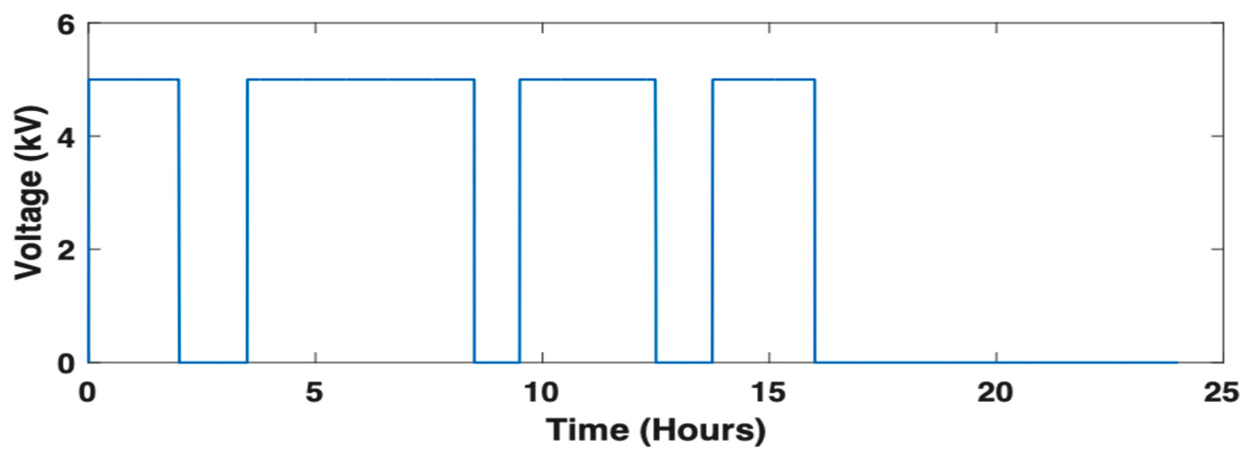
The electrical power system of an electric aircraft is different from a conventional power system since it is energized/de-energized frequently, aligned with flight durations. During takeoff, the DC power system of the aircraft power system is energized and ramped to the operating voltage. The DC power system remains energized until landing (typically 2–5 h). After landing, the power system is de-energized. The DC power system remains de-energized when the aircraft is on the ground (typically 1–2 h). Now, if an aircraft performs multiple trips in a day, the electric stress profile on the HTS cable would be a pulse train. The duty cycle of the pulse train depends upon the flight duration and the time between two adjacent flights.
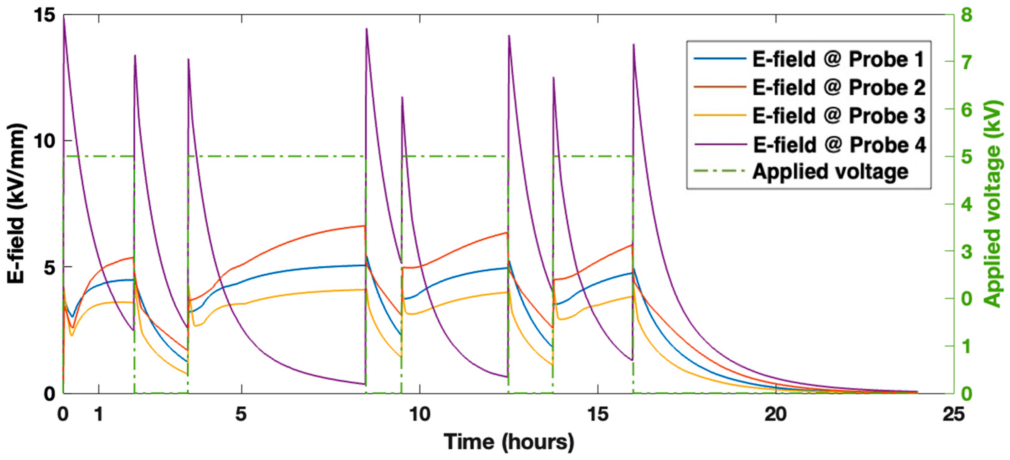
Let us assume a flight schedule of a domestic aircraft, which performs four trips in a day. For the first trip, the flight takes off at 6.00 AM. The flight durations of the four trips are “2 h”, “5 h”, “3 h”, and “2 h 15 min”, respectively. The time durations between the adjacent flights are “1 h 30 min”, “1 h”, and “1 h 15 min”, respectively. The aircraft is at rest for the rest of the time. It is also assumed that the operating DC bus voltage is 5 kV. Based on the aforesaid discussion, the time domain profile of electrical stress acting on the HTS cable of the electric aircraft is depicted in
Figure 4. In the electric stress profile, the HTS cable is energized and de-energized at a rate of 1 kV/s.
2.2. Model Development
To assess the e-field distribution of HTS cable insulation under electrical stress, a 2D axisymmetric model was developed in COMSOL Multiphysics
® 6.1 software. The model consisted of an HTS conductor, lapped tape insulation, and a copper ground layer. In the lapped tape insulation, insulation layers (thickness of 127 µm and tape width of 20 mm) were helically wrapped around the conductor (diameter of 6.35 mm), which leads to the generation of a 1 mm butt gap. It is important to note here that the lapped tape insulation system was modeled considering 50% interlayer overlap. Kapton (ε
r = 3.5), PE (ε
r = 2.3), and PTFE (ε
r = 2.1) were chosen as insulating materials, whereas gaseous helium (ε
r = 1) was chosen as the surrounding medium in the FEM model. The electrical conductivity data (of the aforesaid materials) for the FEM study were taken as the laboratory-measured values (reported in
Table 1)
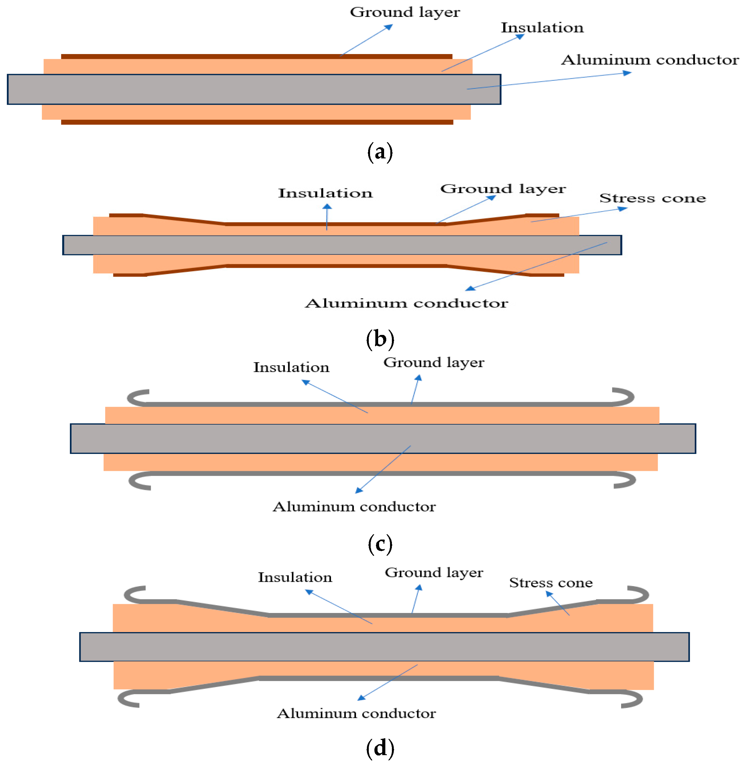
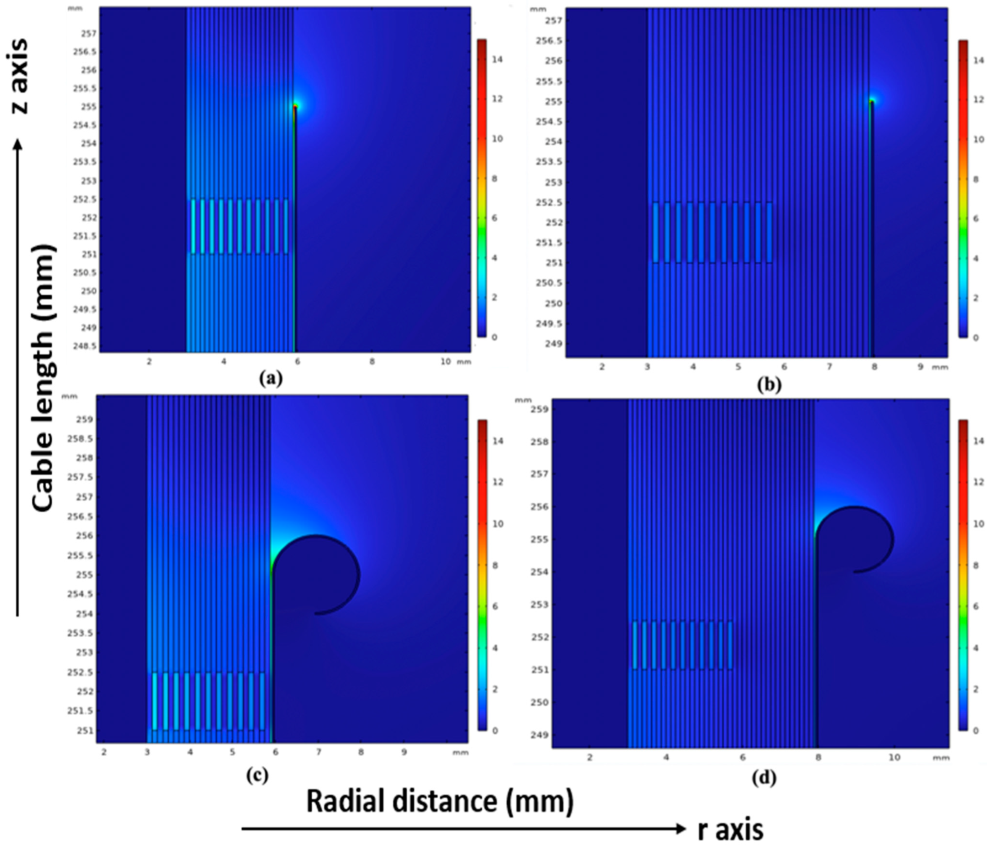
Stress cones were added to the model as a variant to have an idea about the electric field enhancement at the ground termination. The length and thickness of the stress cone are 42 mm and 2 mm, respectively. It yields a pitch angle of <4°.
Additionally, the ground termination geometry in the model was modified to toroidal to understand its effect on electric field enhancement at the ground termination. In the model, a gap of 100 µm was considered between the ground layer and the insulation layer. This is because during the wrapping of the ground layer, a direct bond between the insulation layer and ground layer is not achieved, which allows helium gas to impregnate in this region.
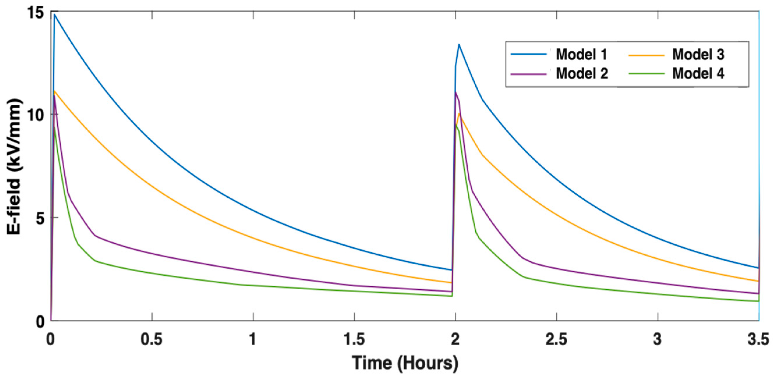
Figure 5a–d show the schematic diagram of the section view of the HTS cable models, i.e., a model without a stress cone (model 1), a model with a stress cone (model 2), a model with toroidal ground (model 3), and a model including stress cone + toroidal grounding (model 4).
Table 2 presents a brief overview of the variables for the FEM study.
The FEM simulation was performed on the AC-DC module of COMSOL Multiphysics
® 6.1 software. During the simulation study, the electrical stress profile (shown in
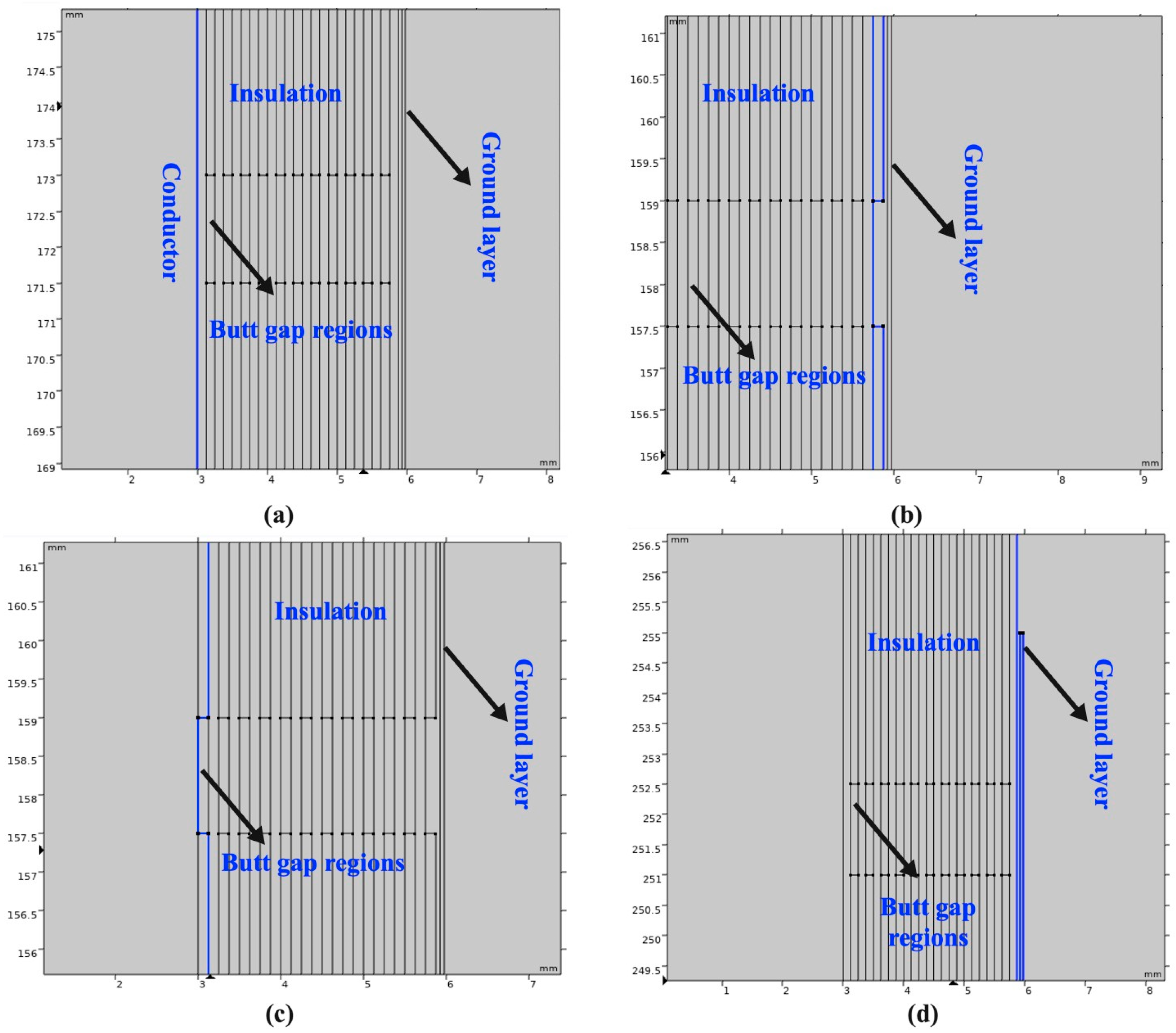
Figure 4) was applied to the conductor while the ground layer was kept at ground potential. An adaptive mesh configuration was adopted in this simulation study. In this configuration, extra-fine mesh with a resolution of 1 µm was applied near ground termination, butt gap–insulation interfaces, and conductor–insulation interfaces. In other regions, a software-generated coarser mesh was employed to reduce computational complexity. Four boundary probes were used to measure the e-field magnitude at four different locations. For this study, they have been labeled as follows: Probe 1 is at the boundary of the conductor surface and the first layer of electrical insulation. Probe 2 is at the boundary of the conductor surface and a butt gap within the first layer of insulation. Probe 3 is the boundary between a butt gap in the last layer of the insulation and the ground layer, and Probe 4 is the boundary at the ground termination interface. At each probe, the e-field magnitude was measured for 24 h in steps of 60 s. The maximum value of the e-field magnitude in the boundary probe was considered for further analysis. In
Figure 6, the location of the boundary probes in the model is portrayed.
4. Discussions
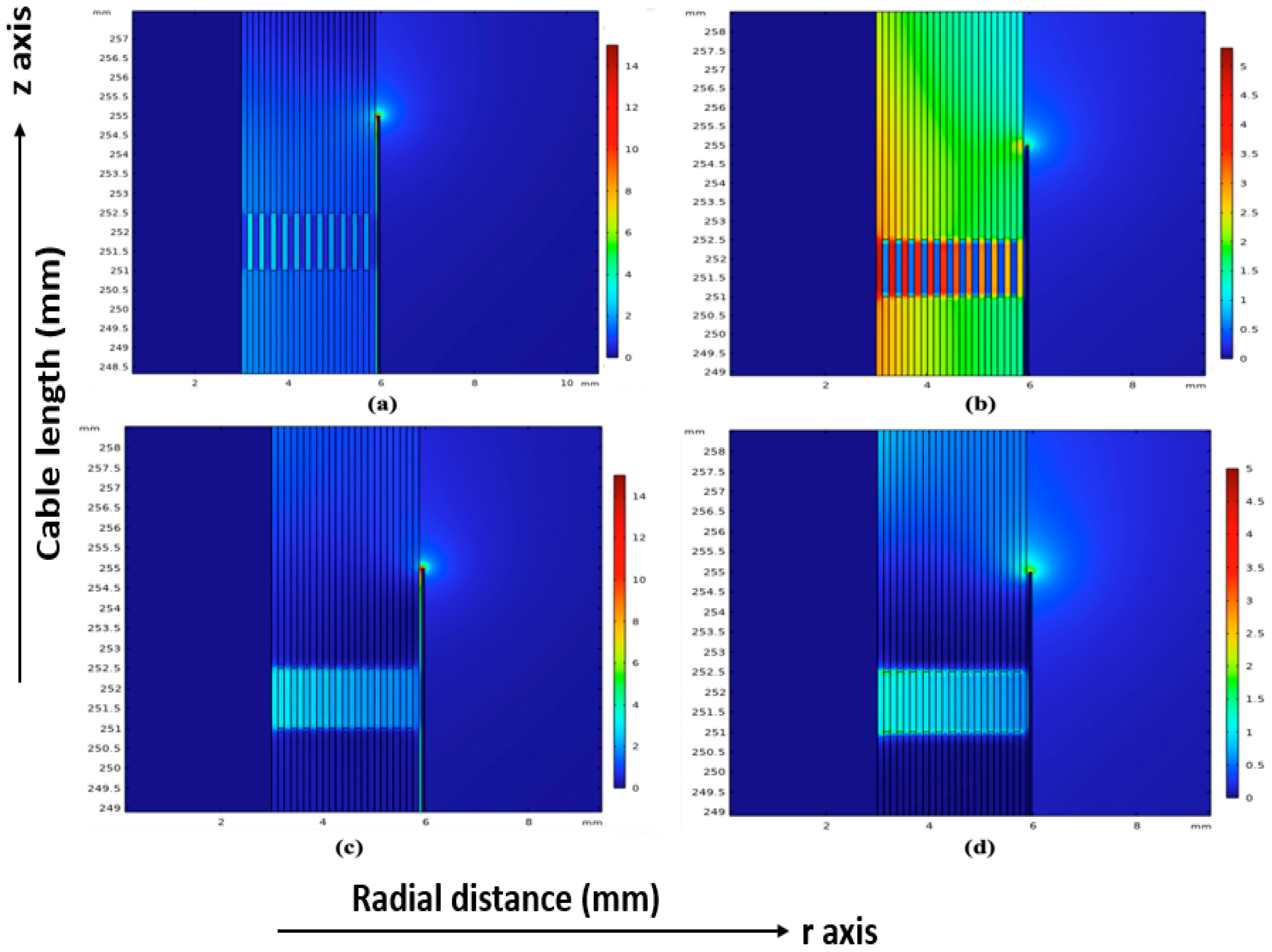
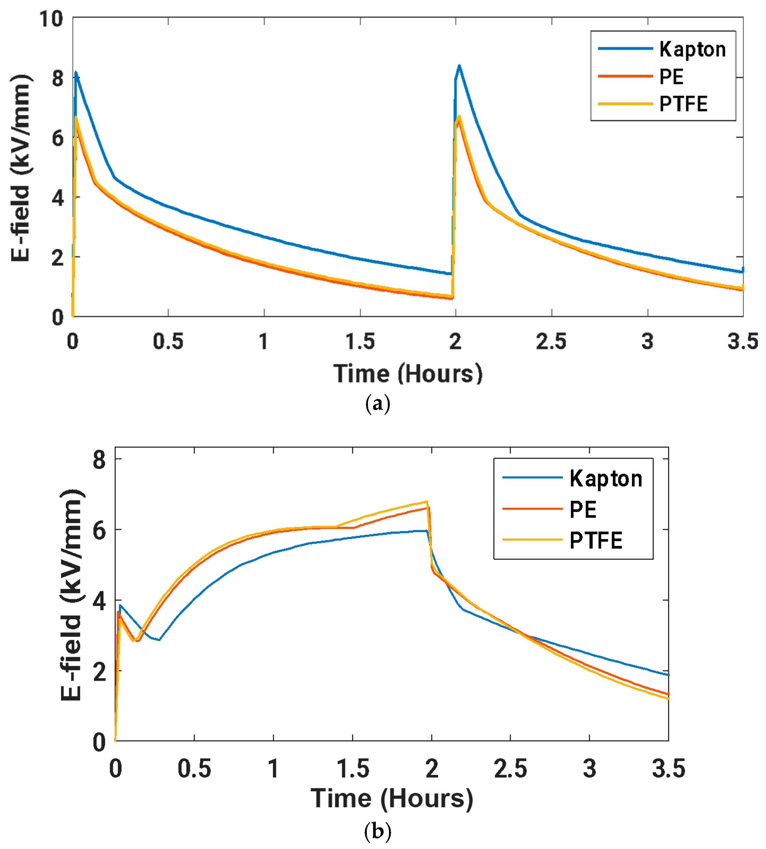
The electric field simulation study presented in this paper suggests that the electric field transients slowly at cryogenic temperatures. During energization/de-energization electric field enhancement is the maximum at the ground termination. With time, the e-field enhanced region shifts from the ground termination to butt gap–insulation regions. However, the e-field magnitude at the ground termination during energization/de-energization is significantly higher than that at butt–gap regions. This is because the peak E-field magnitude at the ground termination is primarily governed by the permittivity of the insulating material and the surrounding gaseous helium. Since the permittivity mismatch at the triple point is the highest, maximum e-field enhancement occurs at the ground termination. As the permittivity of both the solid insulation and gaseous helium exhibits only minor variation with temperature and pressure, the peak E-field remains largely insensitive to changes in gas pressure (0.5–2 MPa) and temperature (60–80 K).
On the other hand, the electrical conductivity of both the insulating material and gaseous helium is strongly dependent on temperature and, for helium, also on pressure. The electrical conductivity decreases as temperature decreases, whereas the conductivity of gaseous helium increases with increasing gas density and pressure. Consequently, lower-temperature and lower-pressure conditions lead to slower charge relaxation, which manifests as a slower transient evolution of the e-field profile. Furthermore, because the steady-state e-field distribution is conductivity-controlled, the steady-state e-field magnitude at the butt–gap insulation interface (probes 2 and 3) becomes higher under lower temperature and lower pressure.
Since the peak electric fields are consistently observed at the ground termination (probe 4) during both energization and de-energization, the grounding technique becomes a critical factor in controlling electric field enhancement under transient conditions. Simulation results indicate that incorporating a stress cone and modifying the ground termination geometry to a toroidal profile significantly reduce the field enhancement at the ground termination. This behavior can be attributed to the smoothing of electric field lines caused by the reshaping of equipotential surfaces when a stress cone and toroidal geometry are used. Moreover, the toroidal ground termination design minimizes geometric sharpness at the triple point, thereby influencing charge accumulation dynamics and enabling a faster transition of the local electric field.
The partial discharge inception voltage (PDIV) is strongly governed by the local electric field magnitude, especially at defects, interfaces, and terminations where field intensification occurs. PDIV is reached when the local electric field exceeds the critical field strength required to initiate electron avalanches within the dielectric medium or along gas–solid interfaces. This relationship can be expressed as
where Emax represents the maximum local electric field stress. Therefore, any reduction in Emax directly increases the voltage level at which partial discharges begin. By reducing the field concentration at the ground termination, the stress cone addition and toroidal grounding geometry effectively lower the peak electric field, thereby shifting the PDIV to a higher value. In other words, a more uniform field distribution increases the dielectric withstand capability before the onset of ionization processes.
Consequently, based on the simulation results, the HTS cable equipped with a stress cone and toroidal ground termination structure is expected to exhibit a higher PDIV due to the inverse relationship between PDIV and electric field magnitude.
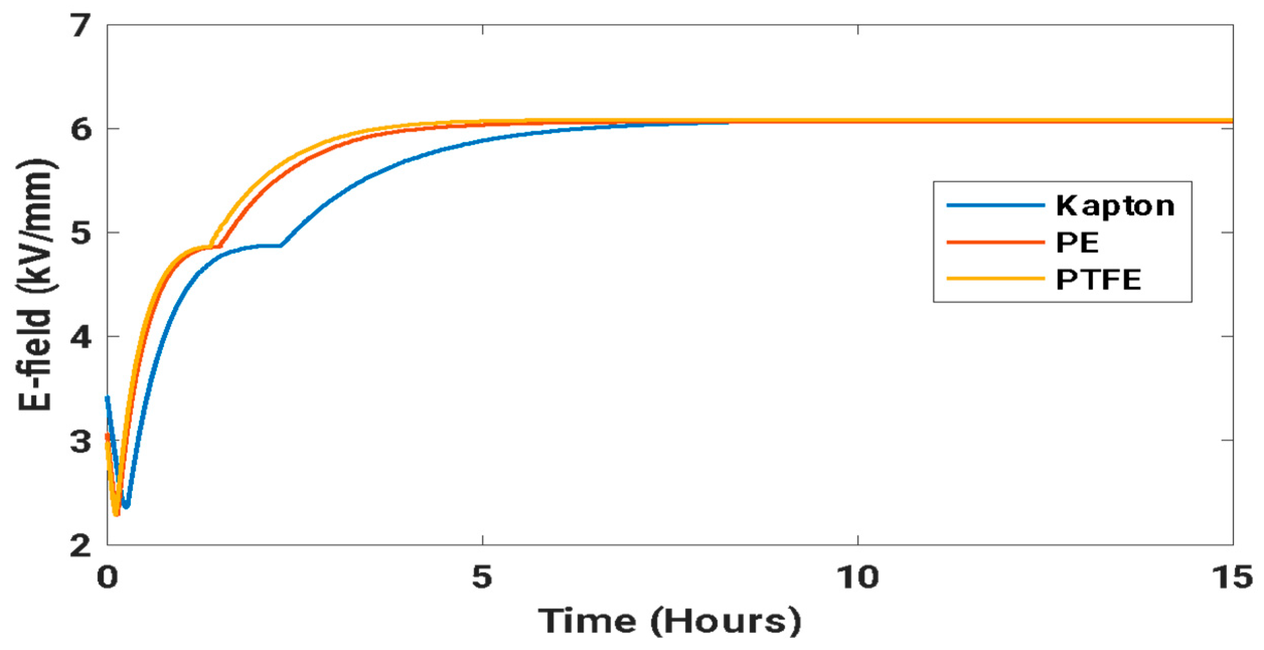
Relative permittivity and electrical conductivity of the material play an important role in the time-dependent e-field characteristics. Due to lower permittivity, PE and PTFE yield lower e-field enhancement during energization/de-energization. So, partial discharge probability during energization/de-energization should be lower for PE and PTFE cables. On the other hand, the transition time constant and the mismatch in transition time constant value between the insulating material and GHe control the e-field profile during the transient phase. The result presented in
Figure 12 indicates that the e-field distribution reaches its steady state value at 5.11 h (for the PE cable), 6.31 h (for the PTFE cable), and 10.08 h (for the Kapton cable). If we consider the steady-state time as 4
, then the transient time constant of the e-field distribution is around 1.28 h (for PE cable), 1.58 h (for PTFE cable), and 2.5 h (for Kapton cable). Due to the higher transition time, the e-field distribution for the Kapton cable never reaches a steady state, as most of the electric aircraft operate in the time range 2–5 h. In this regard, it is important to note that the Kapton cable yields a low e-field magnitude at the butt gap–insulation interface during the phase 2–5 h after energization. Hence, it is expected that the Kapton cable may exhibit less discharge activity (compared to the PTFE and PE cables) before de-energization.
As a continuation of this work, cryogenic performance of Kapton, PE, and PTFE will be investigated for potential application as HTS cable insulation. Lapped tape prototype cables (Kapton, PE, and PTFE as insulation material) will be fabricated in FSU-CAPS according to the design presented in
Figure 5. For toroidal grounding, a braided sleeve will be used. It is well established that the partial discharge inception voltage of the prototype HTS cable is dependent on the e-field magnitude at the ground termination or butt–gap-insulation interface regions [
9]. Hence, to verify the simulation result, partial discharge measurement of the prototype cables will be performed under DC stress in a GHe environment at 77 K and 2 MPa pressurized conditions. The partial discharge measurement setup will be configured in accordance with the IEC60270 standard [
25]. Details about the partial measurement setup under DC are given in [
20]. The partial discharge inception voltage (PDIV) will be considered as the voltage at which there will be at least one discharge pulse (above 10 pC) for 10 consecutive minutes. Furthermore, PD data at extended PDIV voltage will be recorded for 5 h to investigate the electric field dynamics in HTS cable insulation under DC stress and at cryogenic temperature. The experimental data will be correlated with the simulation results presented in this paper.
It is important to note that the present FEM framework does not incorporate full space charge transport equations, such as bipolar charge continuity, mobility-driven drift, injection processes, or trap-controlled charge dynamics. Therefore, the “accumulated charge” referred to in Equation (3) represents only polarization-related displacement charge and conduction effects governed by the material permittivity () and electrical conductivity (). As a result, microscopic charge transport, trapping–detrapping behavior, and interface-controlled injection phenomena are not explicitly resolved. While this approach captures the dominant macroscopic field redistribution, it may underestimate local charge build-up in polymers at cryogenic temperatures.





 ,
,