1. Introduction
Artificial neural networks (NNs) constitute one of the most powerful and flexible tools of modern technology [
1]. Inspired by the structure and functioning of the human brain, NNs are composed of computational units called neurons, organized in layers [
2], and connected to each other to learn representations of complex data. Thanks to their capability to also model nonlinear relations and to generate examples and synthetic data, NNs have been applied with great success in a large variety of fields [
3], such as computer vision [
4], natural language processing [
5,
6], medical diagnosis and medicine [
7,
8,
9].
One of the greatest advantages of NNs is their architectural flexibility [
1,
3]: models such as fully connected NN (FCN), convolutional NN (CNN), or recurrent NN (RNN) can be adapted to a wide diversity of problems simply by changing the structure or parameters. Moreover, thanks to the availability of tools and advanced software libraries such as TensorFlow [
10] and PyTorch [
11], the development and the training of different NN models have become increasingly accessible.
On the other hand, NNs present a few disadvantages which may limit their use. First, they have high computational demand, requiring high computing resources, limiting their application in embedded and low-cost devices. NNs also typically rely on Graphics Processing Units (GPUs) or Tensor Processing Units (TPUs), which provide high computational throughput but can be costly and power-hungry. Moreover, clusters of GPUs can be expensive and are not always available, especially in real-time or portable applications. In addition, NNs based on CPU or GPU have a variable latency, which could compromise their use in applications such as medical diagnostics or robotic control.
In recent years, the adoption of NNs in embedded applications has registered a substantial growth, also due to the need for real-time inferences in contexts where latency, energy consumption, and portability are critical factors [
12,
13]. In recent years, supervised deep learning methods have been introduced to directly map temporal fingerprints to relaxation times maps by either fully connected networks [
7,
8] or convolutional neural networks [
14] or other models. In particular, field-programmable gate arrays (FPGAs) [
15] have established themselves as a particularly suitable hardware platform for the implementation of machine learning models due to their reconfigurable architecture, massive parallelism capacity, and flexibility in managing logic resources [
16,
17].
The implementation of an NN on FPGA can be done at different levels. The most common solution is based on High-Level Synthesis (HLS) tools, which allow software models, like TensorFlow [
10], Keras, and PyTorch [
11], to be converted into FPGA-synthesizable code, often in languages such as C/C++ or SystemC. The alternative route, adopted here, is the direct description of every functional block at the register-transfer level (RTL) in a hardware description language, which requires a substantially larger development effort but leaves scheduling, memory organization, and arithmetic precision under explicit designer control. The trade-off between these two routes, and the point at which it becomes binding on a real device, is the subject of this work.
1.1. Related Work
Among HLS-based toolflows, Vitis AI [
18] and
hls4ml [
19] have gained particular attention in the scientific community, the former mainly for CNNs [
20] and more complex models, the latter mostly in particle-physics applications [
21] requiring rapid inference.
hls4ml generates FPGA firmware starting from pre-trained models, offering a simplified workflow accessible even without in-depth hardware design skills [
19]. Several studies have nevertheless reported that HLS flows introduce a non-negligible architectural overhead in terms of logic-resource usage and latency, together with limited support for non-standard frameworks and devices, insufficient hardware-performance profiling, and reduced flexibility in adapting to rapidly evolving ML architectures [
22,
23,
24,
25].Their high level of abstraction limits fine-grained control over hardware resources, memory management, and timing, which may affect performance and numerical reproducibility in latency-critical applications such as medical image reconstruction [
8,
22,
26], and HLS-generated accelerators may be difficult to reuse across different network architectures and precision requirements.
These limitations are the reason why, in high-throughput acquisition systems requiring deterministic sub-microsecond response, such as the on-the-fly trigger systems developed for high-energy physics experiments [
26,
27], fully custom low-level firmware is still adopted despite the increased development effort. The present work applies the same design philosophy to neural-network acceleration for quantitative MRI based on MRF.
1.2. Contribution
This work proposes a fully customized and modular VHDL framework for FCN acceleration on FPGAs, aimed at enabling systematic and reusable low-level NN design rather than ad hoc, application-specific implementations. Every computational component is implemented at the register-transfer level without relying on vendor IP cores or high-level synthesis tools. The architecture is built around a reusable “base node” that integrates quantization-aware arithmetic, activation, and requantization operations into a compact, parameterizable unit. This design ensures fine-grained control over memory organization and dataflow, enabling deterministic latency and predictable resource utilization, while explicit integer-only operations guarantee numerical consistency with quantization-aware training, making the proposed approach particularly suitable for real-time applications requiring strict timing. The novelty of this work lies in a modular VHDL design methodology based on a reusable hardware node, which can be systematically instantiated to build FCNs of different sizes while ensuring predictable resource utilization and deterministic latency and not in the implementation of a specific FCN accelerator on FPGA per se, since FPGA-based neural network accelerators are already widely used. The methodology is validated through the implementation of an MRF reconstruction network and compared against hls4ml-generated designs under realistic implementation constraints. The main contributions of this paper are: (1) the definition of a reusable and parameterizable VHDL base-node abstraction integrating quantization-aware arithmetic, activation, and requantization operations within a single hardware unit; (2) a deterministic FCN construction method based on controlled replication and scheduling of 16-node processing blocks, allowing for predictable latency and resource usage; (3) the validation of the proposed architecture through the implementation of an MRF reconstruction network and a comparison against hls4ml designs, including synthesis, routing, and timing-closure constraints on the target FPGA board.
The properties targeted by the proposed architecture are also those required by trustworthy cyber-physical systems (CPSs) in a safety-relevant medical imaging workflow, and the design is therefore presented here as a candidate building block for such systems. In quantitative MRI, reconstruction modules may operate as part of a real-time acquisition–processing pipeline, where bounded latency and reproducible numerical behavior are essential. By implementing the FCN directly in VHDL, the proposed framework, integrating an on-chip parameter storage, avoids runtime variability typical of CPU/GPU execution and enables low and fixed-latency inference after timing closure. This control over timing, arithmetic precision, resource allocation, and hardware isolation supports deterministic operation, data integrity, and reliable real-time performance, which are key requirements for trustworthy and secure CPS in medical applications.
2. Materials and Methods
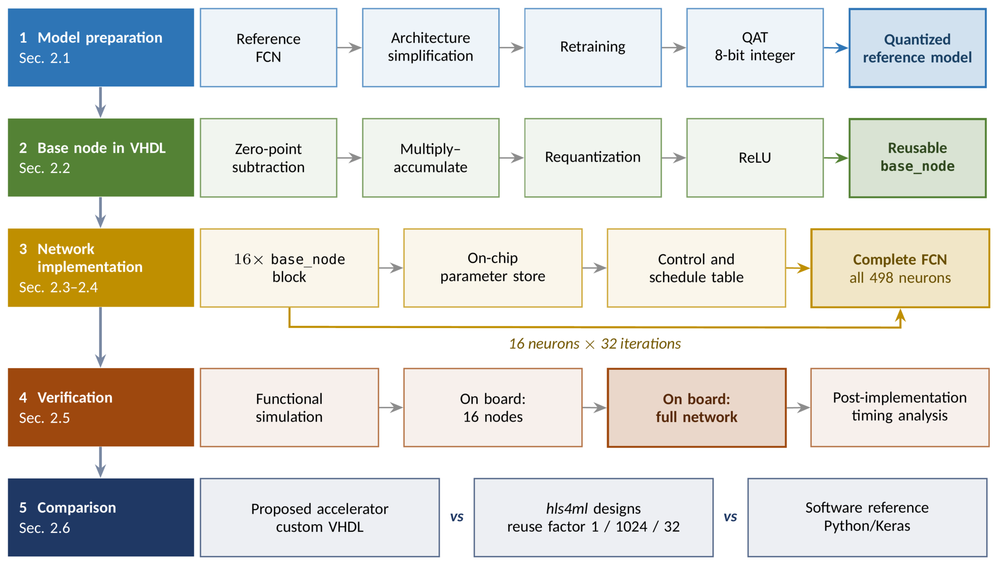
Before describing the individual components, it is helpful to provide an overview of the overall workflow, which is structured into five stages and shown in
Figure 1. (i) The original FCN of Barbieri et al. [
8] is adapted to the resource budget of the target device and retrained, then converted to a full-integer representation through quantization-aware training (QAT), producing the quantized reference model (
Section 2.1). (ii) A reusable base node implementing the integer inference kernel of that model in hardware is written in VHDL (
Section 2.2). (iii) A block of 16 base nodes, an on-chip parameter store, and a control module built on a fixed schedule table are assembled into the complete FCN (
Section 2.3 and
Section 2.4). (iv) The design is verified at four distinct levels, namely functional VHDL simulation, on-device execution of a block of 16 nodes, on-device execution of the complete network over the whole test set, and post-implementation timing and power analysis after place-and-route (
Section 2.5). (v) The same trained model is finally implemented with
hls4ml in three configurations and compared against the proposed design (
Section 2.6).
The current status of firmware development for FPGA allows several approaches for the NN acceleration through hardware. A low-level HDL design approach, in which every firmware block is designed in VHDL without high-level synthesis support, has been selected. The VHDL code was written and managed using the AMD/Xilinx Vivado Design Suite, which was also used for synthesis, implementation, and place-and-route of the proposed architecture. The chosen FPGA board is the Alveo U250 which features 1.7M LUTs, 3.4M of FFs, 12k Digital Signal Processors (DSPs) and 2.6k Block RAM (BRAM). Prior to FPGA deployment, the FCN was implemented and evaluated on a workstation equipped with an Intel® Xeon® W7-2575X CPU, 64 GB of DDR5 ECC memory, and an NVIDIA® T400 GPU. The execution times obtained on this platform are used as a reference for comparison with the FPGA-based implementation.
2.1. Network Adaptation and Quantization
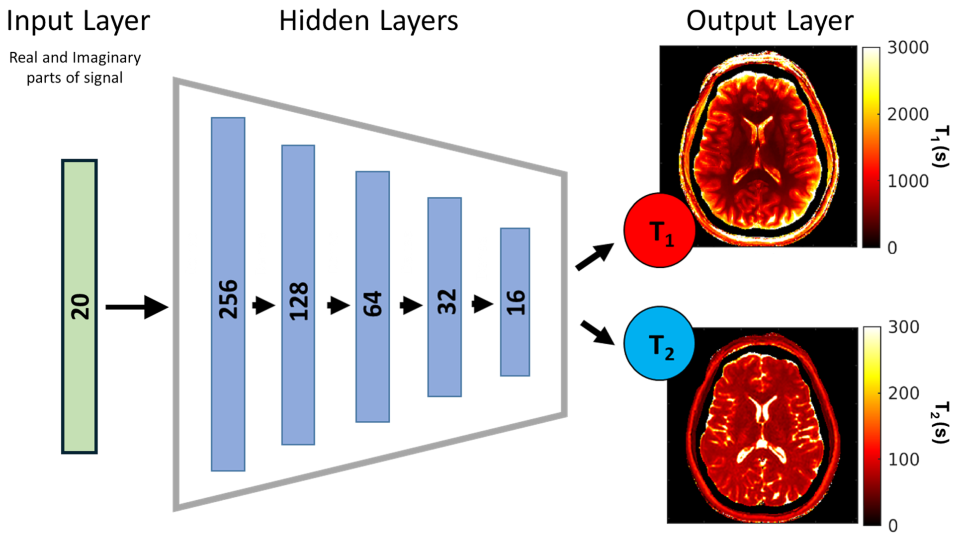
The structure of the original model, derived from Barbieri et al. [
8], was modified to the one shown in
Figure 2: 20 input neurons, hidden layers of 256, 128, 64, 32, and 16 neurons, and 2 linear outputs for T
1 and T
2 (ReLU in all other layers). The NN takes 20 inputs given by the first principal components of the k-SVD–truncated, denoised signal [
7]. The modification consists of removing the two widest hidden layers of the original network, eliminating its largest weight matrices: the
matrix alone has
parameters, yielding a >14× parameter reduction. Because removing >90% of parameters can degrade performance, the reduced topology was validated before hardware design. Both networks were trained from scratch on the same dataset of
simulated IR-FISP MRF signals spanning wide relaxation times, SNRs, and phases, with identical training settings, and reached comparable error.
Finally, since the target architecture operates exclusively on integers, the retrained model was converted to a full-integer representation through quantization-aware training (QAT) [
29,
30], carried out with the TensorFlow Model Optimization Toolkit and exported with the TensorFlow Lite converter. An 8-bit quantization was adopted for both parameters and activations, with 32-bit accumulators.
Table 1 separates the contribution of the two steps on the same 5000-sample test set. The architecture simplification costs
percentage points of global MAPE, whereas the transition to 8-bit arithmetic costs
points, almost twice as much. The accuracy of the deployed model is therefore limited by the numerical representation rather than by the reduced capacity of the network. This model, simplified, retrained, and quantized to 8-bit integer precision, is the one that the hardware architecture implements, and the one against which the numerical correctness of the FPGA design is verified.
2.2. Node Functioning and VHDL Implementation
The most straightforward method to represent the functioning of the human brain is to consider it as a complex network of neurons that receive inputs from other neurons and subsequently transmit information via membrane and action potentials. Based on these principles, the concept of “perceptron” [
31], or artificial neuron, was introduced, which is a mathematical function designed to take a vector of numerical inputs and output their weighted linear combination. A bias is then added to the linear combination and a non-linear activation function is applied to obtain the final neuron activation. Thus, the general function of a single artificial neuron, also called a node, is as follows.
where
represents the single input, weighted by the parameter
;
b is instead the bias and
is the activation function, which is an important function used to introduce non-linearity into the model.
Since Equation (
1) represents the generic operations of each node within a network, it was implemented generically as an independent VHDL package. Thus, it can be used for all the node operations within the desired NN by simply adjusting the input data and configuring the parameters of the node accordingly.
FPGAs natively support integer arithmetic; floating-point operations are possible but cost more logic, latency, and power. Therefore, to meet resource and latency budgets, the node was implemented in VHDL using only integer-only operations. A feasible method of achieving an integer NN is through QAT [
29,
30] on the pre-trained network. Hence, the operations that have been coded in VHDL are intended to simulate the functionality of a QAT network, and are as follows:
where the symbol
q indicates that the variable was previously quantized and
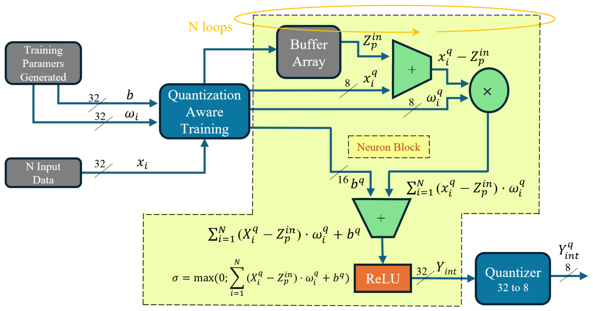
is the zero input point for effective quantization. In this work, an 8-bits quantization was adopted, and in VHDL code, as also represented in
Figure 3, this translates as follows:

Figure 3.
Detailed schematic of the base node implementation used in the VHDL architecture. The quantized inputs
, weights
, and bias
are processed through the integer-only computational pipeline, which performs zero-point subtraction, multiplication, accumulation, and ReLU activation. The quantization-aware operations mirror those used during QAT [
29], ensuring numerical consistency between software and hardware. The final activation
is requantized to 8-bit precision before being propagated to the next stage.
Figure 3.
Detailed schematic of the base node implementation used in the VHDL architecture. The quantized inputs
, weights
, and bias
are processed through the integer-only computational pipeline, which performs zero-point subtraction, multiplication, accumulation, and ReLU activation. The quantization-aware operations mirror those used during QAT [
29], ensuring numerical consistency between software and hardware. The final activation
is requantized to 8-bit precision before being propagated to the next stage.
The result of the weighted sum in Equation (
2) can easily reach 32-bit word representation. To be given as input to the following levels of the NN, the output number
must be quantized to 8 bits. The quantization of the output in Equation (
2) is realized in 6 steps and can be summarized in the following function:
Initially, the process multiplies by an integer scaling factor
. Following that, rounding up to the nearest integer is achieved by adding
, where
n represents a shift factor. At this stage, the computation results are maintained in 64 bits to prevent overflow, and they are subsequently shifted right by the
division. Next, the output zero point
gets added to the shifted value. In the final step, this number is restricted to fit within the
range
and then converted to the appropriate signal type in VHDL.
In this work, the Rectified Linear Unit (ReLU) activation function was selected for its simplicity within the base node package and is implemented as a straightforward if condition:
The modularity of the VHDL block allows one to use the node as a generic entity in different NN contexts, simply modifying the input parameters such as weights, biases, zero-points, and scale factors.
To test the proper functioning of the implemented package for base node calculations, 16 nodes were completely mapped onto the FPGA board. Both hardware and software implementations used the same inputs, weights, and biases, and Python (3.11.10) and FPGA results were then compared.
2.3. Fully Connected Network Implementation
The adapted and quantized network described above provides the first practical motivation for designing an efficient hardware realization of dense layers on FPGA.
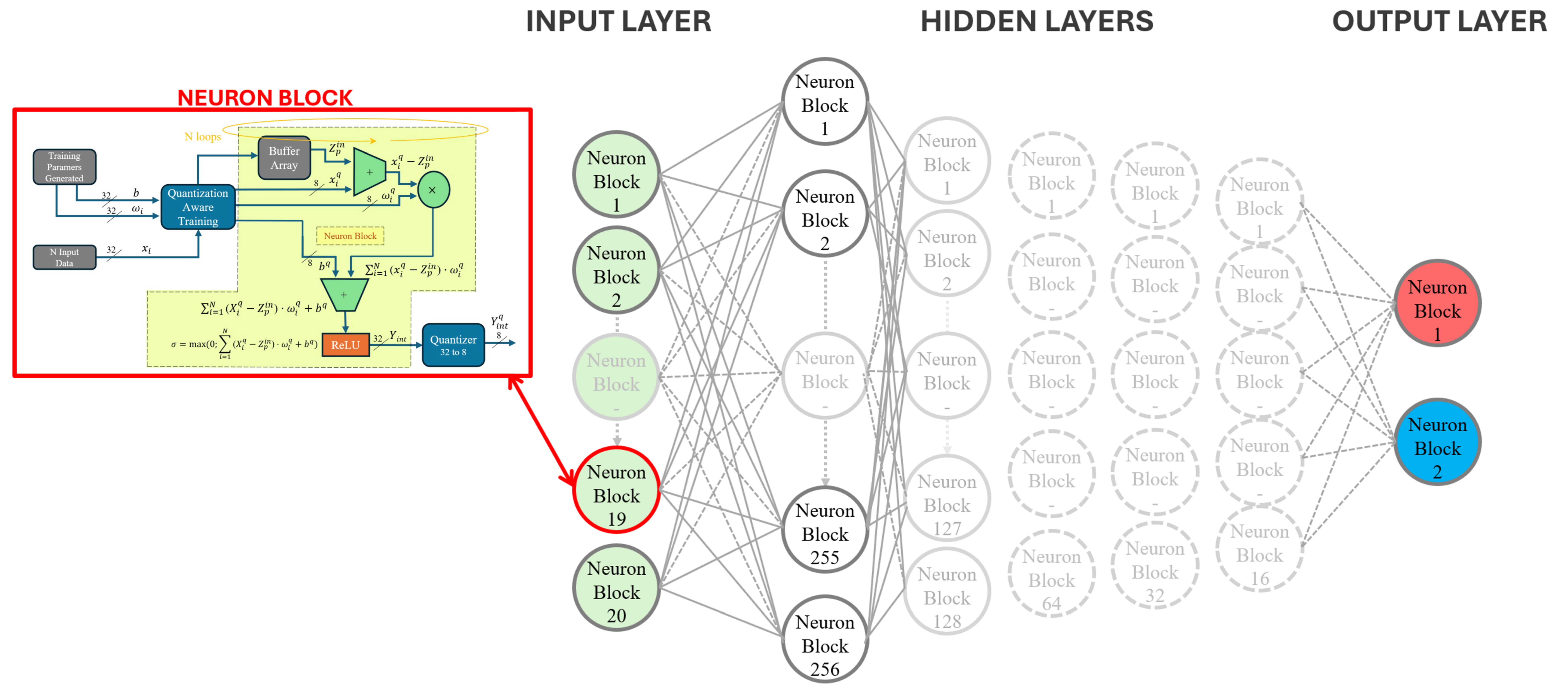
Having defined the simplest computational unit, i.e., the node, a complete NN can now be constructed consisting of nodes arranged in several layers. The very first is defined as the input layer, the final one is the output layer, and those in between are called hidden layers. In this case, each layer receives as input a vector that contains the outputs of the nodes in the previous layer. If every neuron in a hidden layer is connected to all the neurons in the previous layer, as shown in
Figure 4, then such an arrangement is called an FCN.
To optimize the FPGA implementation and find a trade-off between parallelism and logical resources consumption, in the proposed FPGA architecture, the FCN has been implemented by instantiating a single block of 16 base nodes in hardware and iterating on it, in time multiplexing, for the whole network: the 498 neurons are partitioned into 32 groups of at most 16, so that the hardware cost is that of 16 neurons while the network behaves as if all 498 were present.
The specific value of 16 was selected on the basis of three quantitative considerations. First, the arithmetic cost of the block is set by the product of its width and of the largest fan-in it must sustain: with 16 nodes and a widest layer of 256 inputs, the multiply–accumulate array requires DSP units, plus four per node for the 32-bit requantization multiplier, that is, the 4160 units, corresponding to of the device. Doubling the block width to 32 nodes would require 8320 DSPs (67.7% of the available resources), substantially increasing resource utilisation and reducing the headroom available for placement and routing. The 16-node configuration was therefore selected as a more conservative design point, providing sufficient parallelism while retaining a greater resource margin for timing closure. Reducing it to 8 would double the length of the schedule and hence the inference latency. Second, 16 divides exactly all the layer widths of the network (256, 128, 64, 32, 16), so that the partition never crosses a layer boundary and each layer is assigned a whole number of groups. Third, a block of this width keeps the fan-out of the parameter-selection logic within a range that place-and-route can absorb without congestion.
The control module coordinates the FCN execution and is responsible for:
Input loading: activations from the previous layer are gathered into a buffer array, ensuring synchronous data transfer at each clock cycle;
Weight and bias management: parameters are retrieved from the dedicated internal memory block, where they are preloaded and organized in hierarchical matrices tailored to each layer’s dimensions;
Pipeline control: the computation is managed by two counters, which regulate address generation, layer transitions, and the temporal sequencing of input/output storage;
Layer parameterization: quantization-related parameters such as scale factors, zero-points, and shift factors are updated dynamically at each layer, ensuring that the integer-only arithmetic remains consistent with the QAT;
Output collection: the computed activations are stored in another buffer array, either to be propagated to the next layer or to serve as the final network output.
Compared to fully automated HLS tools, this low-level VHDL code offers much greater control. Every step of the computation—from weight memory placement, through scheduling multiplications and additions, to rounding strategy in requantization—is explicitly defined. Unlike programmable devices such as GPUs and CPUs, FPGAs are internally synchronized with a clock signal that defines what happens step by step. For this reason, the system guarantees deterministic latency, precise use of resources, and the ability to fine-tune numerical precision adapted to application-level constraints. This kind of control is typically not present or limited in HLS-generated designs, where the optimization is left to rely on the heuristics of the compiler and the libraries.
The computation of a layer proceeds deterministically. At the beginning of each clock cycle, input activations are loaded into a buffer array. Each node calculates the weighted summation of the inputs, adds the corresponding bias, performs requantization steps, and applies ReLU activation. Outputs of the 16-node block are produced in parallel and saved into the corresponding positions in the output vector. Once the outputs of a layer have been completed, the system updates the quantization parameters and begins computation for the following layer without host intervention.
This design shows the advantages of a custom-designed architecture: it is deterministic, scalable, and modular. Within the limits imposed by the available FPGA resources, memory bandwidth, routing complexity, and timing-closure constraints, larger FCN architectures can be constructed by duplicating the 16-node blocks or by chaining multiple instances together, while maintaining the same deterministic execution model and explicit control over arithmetic precision. Besides, interoperability with on-board FPGA memory ensures that weights and biases are correctly distributed to the computational units, reducing Peripheral Component Interconnect Express (PCIe) transactions and improving throughput.
2.4. FPGA Internal Memory
Another key aspect in the FPGA implementation of NNs is related to memory management. Weights and biases need to be provided to the computation units at each clock cycle during inference, and using external PCIe transfers would lead to high latency and bandwidth usage. To overcome this issue, a custom memory block was created to store all the parameters locally inside the FPGA and to make them available efficiently during computation.
The module has two sub-modules dedicated to weight and bias storage, respectively. They are both instantiated in read-only mode for inference, because weights and biases are pre-loaded before execution. Data are represented as std_logic_vector first and then cast into signed integers to be compatible with arithmetic operations defined in the base_node module.
The design of the memory is guided by the following principles:
Hierarchical organization of weights: parameters are grouped according to the size of each layer. For example, the first layer requires 256 neurons with 20 inputs each, while subsequent layers progressively reduce in size down to 2 neurons with 16 inputs. This organization guarantees compact storage and predictable addressing.
Efficient bias handling: biases are preloaded into dedicated registers and synchronized with the computation pipeline, ensuring that each node receives its corresponding parameter in the correct cycle.
Parallel access: multiple weights can be made available simultaneously through the use of generative constructs, feeding the 16-node computation blocks without additional multiplexing overhead.
Explicit data conversion: the casting from std_logic_vector to signed guarantees consistency with the quantization scheme adopted, avoiding mismatches between memory representation and arithmetic logic.
Reduced host transfers: by preloading all parameters within the FPGA, communication via PCIe is minimized, improving both latency and energy efficiency.
The other part of the memory management strategy is the method implemented in the Top_module to operate sequentially. At every rising edge of the clock, the design iterates through the 16 nodes and updates both their biases and weights according to the current cycle counter: the weights are progressively loaded in blocks from the global weights matrix into local registers, with different time intervals corresponding to different portions of the layer. At the first rising edge of the clock, the registers are reset back to their initial values, and then later cycles fill in 20, 256, 128, 64, 32, then 16 entries, filling unused positions with zeros if necessary. This hierarchical loading plan follows the decreasing size of the layers and ensures that only the appropriate subset of the weights is active during any one cycle.
Biases are handled the same way: they are initialized at the beginning of each calculation, and while the counter is incremented, they are loaded in from the preloaded bias matrix. This design guarantees that every node sees the correct weights and bias in parallel with the processing pipeline.
The memory module, coupled with the Top module of the FCN, supports the network to be executed in autonomous mode completely within the FPGA, realizing the modularity of design of this work.
2.5. NN Performance Evaluation
To evaluate the performance of the implemented NN, a dataset consisting of 5000 samples was used as input for both the software-based and hardware-based network implementations. Each of these samples corresponds to a simulated MRF signal generated for a single pixel, representative of an MRF image. In other words, every data point in the set models the temporal signal evolution that would be measured from one pixel under specific tissue and acquisition conditions. Since the implemented model is an FCN, the reconstruction process is performed in a pixel-wise manner, meaning that each pixel is processed independently and no spatial information from neighboring pixels is used. Consequently, each input sample is representative of a generic image pixel, and the complete reconstruction of an image can be obtained by applying the same network to all pixels individually. This makes the chosen dataset representative of the entire and domain, despite being composed of independent samples.
The simulated MRF signals were generated following the methodology described in [
8]. These works describe how to obtain realistic MRF time courses by incorporating appropriate tissue parameters (such as
and
relaxation times) and acquisition settings (such as flip angle patterns and repetition times). In particular, the simulated
and
values were sampled uniformly and independently over a wide physiological range (
: [0.0438–3.9990 s] and
: [0.0017–2.9990 s]), covering relaxation times representative of different tissue types and anatomical regions, with the same forward model, the same IR-FISP pulse sequence, and the same augmentation and preprocessing chain used for the training data. This choice was made to increase the robustness of the trained FCN and avoid specialization to brain-only applications. The 5000 samples were generated independently of, and are disjoint from, the
signals used to train the network, and were never seen by the model during training or validation. Using this common set of 5000 simulated MRF signals—referred to as the 5000-sample dataset in the rest of the paper—for the ground truth, the floating-point model, the quantized software model, and the FPGA implementation enables a direct comparison with the tested hls4ml configurations.
The validation was carried out at four distinct levels:
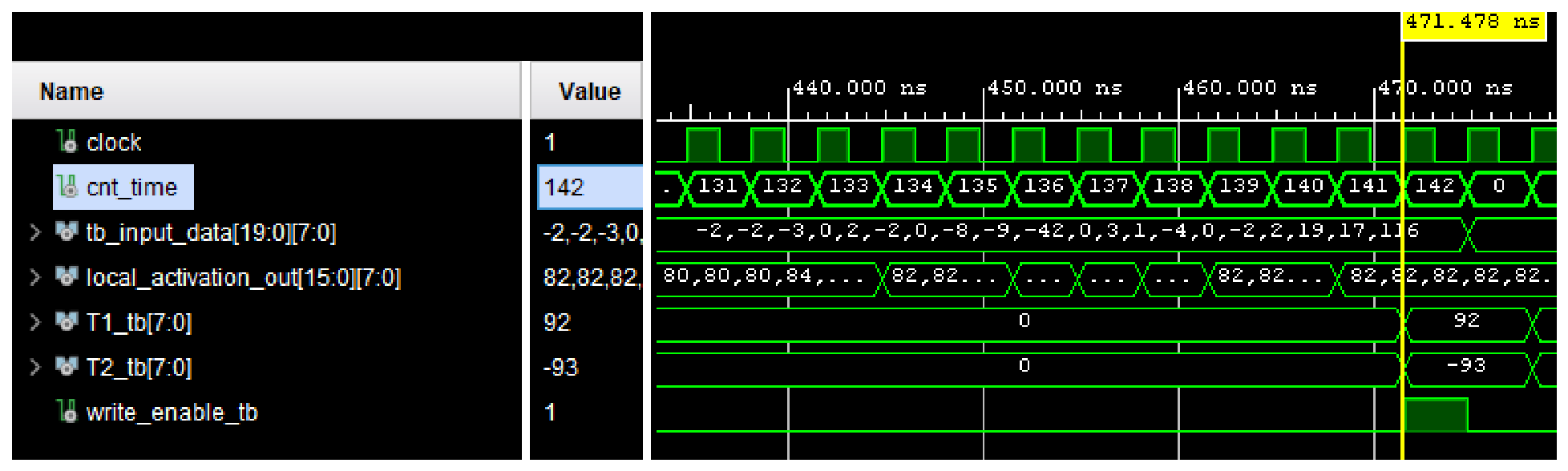
(i) Functional simulation. A behavioral VHDL simulation of the complete FCN reproduces the logical behavior of the firmware exactly, including the processing sequence and the logical timing of operations, but it does not reproduce the physical propagation delays through the FPGA fabric. It is therefore used to establish functional correctness, and the cycle count of an inference and the latency it yields are expressed at the nominal simulation clock of .
(ii) Module-level on-board verification. A block of 16 base nodes was mapped onto the physical device and its outputs compared, for identical inputs, weights, and biases, against the software reference. This step verifies the arithmetic of the elementary unit but it is not sufficient to establish the correctness of the entire network.
(iii) Full-network on-board execution. The complete FCN was configured on the Alveo U250 and executed on the physical device over the entire 5000-sample test set. The input samples were streamed to the accelerator and the integer outputs were read back and compared, before dequantization, with those produced by the reference 8-bit quantized model executed in software by the TensorFlow Lite integer kernel. This is the level at which the expression “deployed on the target FPGA” is used in this work: the design was synthesized, placed, routed, loaded onto the device, and run on the complete test set.
(iv) Post-implementation analysis. After place-and-route, static timing analysis was used to determine the maximum achievable clock frequency and to verify timing closure, and vectorless power analysis to estimate power consumption. All latency and power values reported for the implemented design derive from these reports and are estimates produced by the design tools, not metered measurements.
Latency, resource utilization, numerical error, and power consumption were selected as evaluation metrics because they directly determine the feasibility of FPGA accelerators in real-time and embedded contexts, where timing determinism, hardware footprint, numerical fidelity and energy efficiency are equally critical. The Python/Keras execution time used as a baseline was measured on the workstation over the complete 5000-sample dataset rather than on a single inference, because software execution time varies from run to run due to scheduling, cache behavior, and runtime overhead.
The design was developed with the AMD/Xilinx Vivado Design Suite 2022.2, and the software reference with TensorFlow/Keras 2.15.0 and the TensorFlow Model Optimization Toolkit 0.8.0. Quantization is symmetric per tensor for the weights and asymmetric per tensor for the activations, with 8-bit parameters and activations and 32-bit accumulators, as described by Equation (
3).
2.6. Three-Way Evaluation Pipeline
In order to provide a comparison with existing FPGA-oriented toolflows, the same FCN model was also implemented using the
hls4ml framework [
19]. The conversion started from the trained Keras model, leaving the default
hls4ml configuration parameters unchanged. Network parameters and activations are automatically mapped to fixed-point representations with a precision of 8 bits, with wider accumulators for intermediate sums. In this way, the generated design reflects a standard and widely adopted baseline for NN implementation on FPGA, without introducing additional manual optimizations that could bias the comparison.
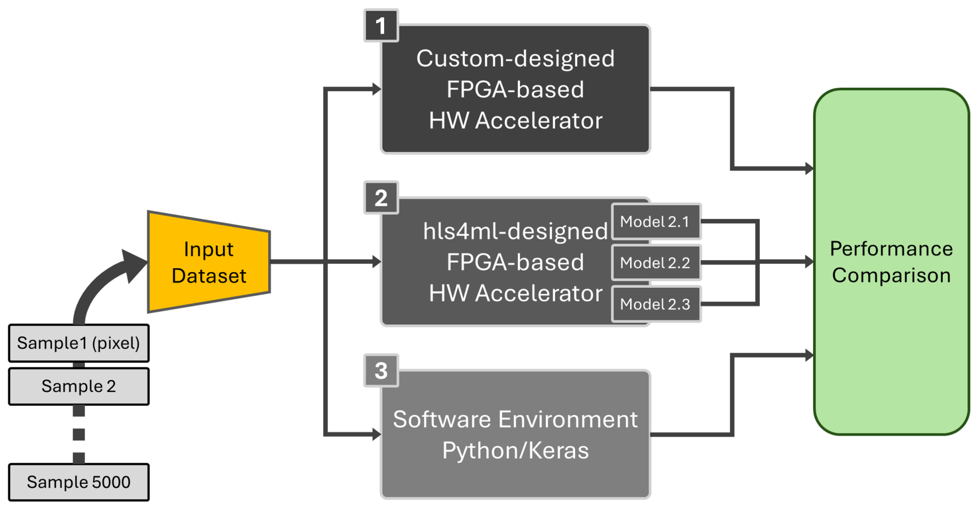
Three different
hls4ml implementations were tested. In the first case (model 2.1), the entire network is implemented fully in parallel, where all nodes are instantiated simultaneously. The second (model 2.2) applies a strong serialization, so that only a very small fraction of the nodes is physically implemented and iterated over in time. The third (model 2.3) adopts an intermediate configuration chosen to mirror the proposed architecture, which instantiates 16 nodes of the full network and processes the remaining nodes sequentially. As illustrated in
Figure 5, the proposed VHDL implementation is evaluated against the
hls4ml implementations and the software-based model in terms of latency and resource usage.
4. Discussion
The primary contribution of this work is not the implementation of a single FCN on FPGA, but the definition of a reusable low-level hardware design methodology that allows FCNs to be systematically constructed from a parameterizable node abstraction. This introduces a new approach to the use of NNs for quantitative MRI image reconstruction, based on hardware-accelerated inference of an FCN network for MRF. The success of this approach could open perspectives for the development of embedded systems for the real-time reconstruction of quantitative maps, to be applied directly in the context of MRI acquisitions in clinical settings. FPGAs have shown to be particularly suitable hardware platforms for the implementation of deep learning algorithms due to their flexibility in configuration that can be tailored to specific computational patterns, enabling optimized parallelism, low-latency processing, and efficient use of on-chip resources while maintaining relatively low power consumption. Here, we propose a modular approach for implementing FCNs on FPGAs based on a node function that already integrates all required operations, so that one only needs to instantiate this node an appropriate number of times to construct the full network, thereby greatly simplifying the design and implementation of FCNs.
4.1. Numerical Accuracy Evaluation
The comparison carried out on the device over the entire 5000-sample test set showed agreement on all 5000 integer output T1 and T2 couples, before dequantization. Every int8 value computed by the accelerator is the same value that the reference quantized model produces for the same input. The residual error of the deployed system is therefore entirely the error of the quantized network, and the hardware adds nothing to it.
In line with previous deep-learning MRF studies, reconstruction performance was evaluated using MAPE, MPE, and RMSE with respect to the ground truth. Since the accelerator reproduces the quantized model exactly, the question of accuracy moves entirely from the hardware to the numerical representation, and
Table 1 locates it precisely: removing the two widest hidden layers costs
percentage points of global MAPE, whereas the transition to 8-bit arithmetic costs
, almost twice as much. The dominant source of the residual error is therefore the numerical representation, not the architecture simplification and not the FPGA implementation. The same conclusion follows from the MPE, which remains within a tenth of a percentage point of zero for
but reaches
for
: quantization introduces a systematic overestimation, concentrated in the lowest decile of the
range where the
output step is a large fraction of the value being represented. This bias is deterministic, and is therefore consistent with the reproducible nature of the architecture. More importantly, it identifies a well-defined solution: widening the output representation beyond eight bits, an intervention confined to the requantization of the last layer that would leave the base node, the memory organization, and the scheduling unchanged and would use a negligible fraction of the available resources.
It is worth being explicit about what the FPGA implementation is and is not intended to do: it does not improve the intrinsic predictive accuracy of the neural network, but deploys it in a deterministic, verifiable, and bounded-latency hardware form. From a quantitative MRI perspective, relative errors in the 8–15% range for
mapping are commonly reported in vivo [
32,
33,
34], so that the
observed on the synthetic test set falls within the range in which quantitative-imaging applications already operate. This is a limitation of the numerical representation of the model, not of its hardware realization, and it is precisely the component that widening the output stage would remove.
4.2. Post-Implementation Timing and Power Analysis
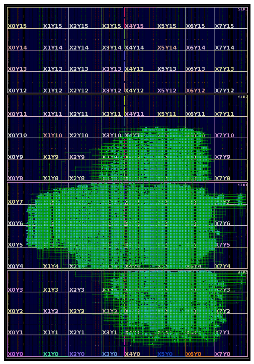
After successful implementation and deployment of the FCN on the target FPGA board, post-implementation resource usage analysis (
Table 3 and
Figure 7) shows the efficiency and scalability of the proposed FCN architecture. The design occupies only 12.29% of the available LUTs and 6.51% of FFs, indicating that the control logic and data path are implemented with a limited footprint. The usage of LUTRAM is negligible, confirming that the architecture does not rely heavily on distributed memory resources. A more significant portion of resources is represented by the DSP blocks, with 33.85% utilization. This behavior is expected, as the FCN computation is dominated by multiply–accumulate operations. The DSP usage grows in a predictable and regular manner with the number of instantiated nodes, making performance and scaling easy to control during architectural exploration.
Post-implementation timing analysis indicated a maximum operating frequency of
. This resulting frequency is lower than the targeted
. However, an acceleration factor of
is achieved compared to the software. An additional advantage of the selected operating point is power efficiency. Increasing the clock frequency on FPGA platforms leads to an approximately linear increase in dynamic power consumption. According to the FPGA post-implementation power analysis report, operation at
is associated with an estimated power consumption of
. Thus, the FPGA implementation suggests an energy-efficiency advantage of about four orders of magnitude for the 5000-sample dataset. In fact, considering a typical MRF brain slice composed of approximately
pixels, the estimated reconstruction time is about
on the workstation and
on the FPGA. As shown in
Table 4, this corresponds to an energy consumption of approximately
and
, respectively, further highlighting the significant advantage of the FPGA-based implementation in both latency and energy efficiency, demonstrating the potential of the proposed approach for energy-efficient deployment in large-scale or real-time medical imaging applications. Both sides of this comparison are estimates and not metered measurements: the FPGA value derives from design-tool power analysis, which uses circuit-level switching activity to predict dissipation and does not account for board-level power-delivery losses or host idle power, and the workstation estimate derives from the rated power of the platform rather than from a wall-power measurement taken during execution. The relative comparison in
Table 4 is reported here as an order of magnitude.
Unlike software implementations on CPU or GPU, where execution time varies depending on memory access patterns, scheduling, and parallel workload, the FPGA design operates with a fully deterministic pipeline, and each inference is completed with constant and predictable time. It is worth being precise about the origin of this property: the latency is not observed to be constant, it is constructed to be constant, since the schedule is encoded in a constant table fixed before synthesis and the entire parameter set of parameters resides on-chip, so that no transfer over the PCIe interface takes place during inference. The number of clock cycles required by an inference is therefore a property of the design and not of the data. The acceleration factor of actually achieved after implementation, together with this fixed and predictable latency, is what makes the solution relevant for real-time applications.
From a trustworthy cyber-physical systems perspective, the deterministic behavior of the proposed FPGA implementation is as important as its acceleration factor. In a real-time MRI acquisition/reconstruction workflow, bounded latency and reproducible numerical behavior are essential for reliable operation, while verifiable hardware execution and controlled on-chip data and parameter storage can contribute to system integrity and security. These are properties that would facilitate integration into safety-relevant medical imaging systems. No system-level verification, no interfacing with acquisition hardware, no safety or security analysis, and no clinical evaluation have been performed in this work, as they fall beyond the scope of the present study. The discussion of clinical and safety-critical scenarios in this paper should be read as a statement of potential application rather than of demonstrated capability.
4.3. Scaling Behavior
Only one network size and one degree of parallelism were implemented in this work, so that the scalability of the architecture cannot be claimed as an experimental result. It can, however, be stated as an explicit model, because the composition of the resource usage is known by construction. The DSP occupation, which is the resource that will be exhausted first, decomposes as
where
is the width of the node block and
the largest fan-in it must sustain, the four additional units per node being the 32-bit requantization multiplier. The number of clock cycles of an inference is likewise fixed before synthesis and is given by
with
the number of neurons of layer
ℓ and
d the constant drain of the node pipeline at each layer transition, so that the inference latency is
.
Two consequences follow, and they are the reason why the two directions of growth can be quantified before implementation. Adding layers, or widening a layer beyond
W, lengthens the schedule of Equation (
5) and leaves the arithmetic occupation of Equation (
4) unchanged; it costs latency, not DSPs. Widening the node block, instead, costs DSPs in proportion to
W and reduces the latency correspondingly. The depth of the network is therefore absorbed by time multiplexing and does not enter the resource budget at all, whereas
and
W determine it entirely. What Equations (
4) and (
5) do not predict is timing closure, which depends on placement and routing and can become binding well before the resource budget does; the maximum achievable frequency of a scaled design must therefore still be established by implementation. Within these limits, and provided that the parameter set continues to fit on-chip, the framework can be extended to larger FCN configurations in a controlled way.
4.4. hls4ml Model Analysis
As a final point of comparison, the proposed VHDL architecture was evaluated against an implementation generated with the hls4ml framework, starting from the same quantized Keras model and using default configuration parameters. Although hls4ml is designed to simplify the deployment of NNs on FPGA, the practical realization of the considered FCN turned out to be non-trivial and required substantial effort to obtain meaningful synthesis results.
As a first attempt, the entire network is implemented fully in parallel (model 2.1), where all nodes are instantiated simultaneously. This configuration was obtained by using all the default
hls4ml settings, using it as a pure automated tool. As shown in
Table 5, with these configurations, the design requires more than the available logic resources, showing how a brute-force parallel mapping of the FCN is not practical for networks of this size, and results in the impossibility of deploying such a model on the FPGA board. To reduce resource usage, a second
hls4ml model (model 2.2) was built, using a strong serialization factor of 1024. In this way, only a very small fraction of the nodes is hardware-developed and used iteratively to cover all the operations of the FCN. Whilst drastically reducing the necessary resources, it still requires
of the available LUTs. The reuse-1024 implementation successfully completed place-and-route. However, timing closure was not achieved, with a WNS of
ns affecting more than 38,000 timing endpoints. This indicates that, although aggressive serialization greatly reduces DSP utilization, the resulting architecture introduces long critical paths that prevent operation at the intended clock frequency.
Finally, model 2.3 was tested to provide an additional comparison between the proposed modular VHDL approach and
hls4ml. As shown in
Table 5, also in this case the implementation on the FPGA board failed to complete. Consequently, the reported latency of
and maximum frequency of
for model 2.3 cannot be considered achievable without substantial redesign or additional optimization. Although the overall LUT utilization remained at only 42%, implementation still failed because the router reported a global congestion level of 7, indicating that routing complexity rather than raw resource availability became the limiting factor. In contrast, the proposed custom VHDL architecture successfully completed place-and-route and achieved timing closure at
. The placement shown in
Figure 7 confirms a controlled resource utilization with available device headroom, supporting the scalability and practical deployability of the design.
To sum up, none of the three hls4ml configurations produced a working bitstream, and consequently no hls4ml baseline could be executed on the device. The comparison reported here therefore documents that, for this network, on this device, and under the default and reuse-factor configurations tested, the automated flow did not reach a deployable implementation while the proposed custom design did. It does not establish that the proposed architecture is superior to hls4ml in general: a different device, a smaller network, or a more extensive manual tuning of the hls4ml directives, of the precision settings, or of the partitioning strategy could well yield a working and competitive design, and no such exploration was attempted here.
5. Conclusions
This work presents a fully custom FPGA implementation of a quantized FCN for MRF map reconstruction, built around a modular and reusable VHDL node module architecture. Rather than targeting a single ad hoc accelerator, the proposed approach defines a systematic methodology for constructing FCNs with deterministic, pipelined inference and fixed latency, while providing substantial acceleration over CPU-based execution.
The design was synthesized, placed, routed, configured on the target Alveo U250 board, and executed on the device over the entire 5000-sample test set, where it agreed with the reference 8-bit quantized model on every one of the 5000 integer output T1 and T2 couples. The accuracy of the accelerator, a MAPE of on and on with respect to the ground truth, is therefore not merely comparable to that of the software model but identical to it, and the residual error is attributable to the 8-bit representation rather than to the hardware. After place-and-route, the design closed timing at , giving a fixed per-inference latency of 1.14 μs and an acceleration factor of relative to the software baseline, with LUT and DSP occupation. The associated energy-efficiency figure of should be interpreted as an indicative estimate based on design-tool power analysis and on the rated power of the reference workstation, and not as a direct wall-power measurement.
The comparison with the hls4ml framework was carried out under the default and reuse-factor configurations of the tool, and none of the three produced a deployable design on this device for this network, whereas the proposed architecture did. This supports the usefulness of a low-level architectural approach when strict timing and implementation constraints apply, but it is a statement about this case study and not a general claim of superiority: automated toolflows remain the appropriate choice for smaller networks, for rapid design-space exploration, and whenever development effort is the dominant constraint.
5.1. Limitations
Four limitations should be made explicit. First, the validation was carried out entirely on simulated MRF signals produced by the same forward model used to generate the training data, so the accuracy values reported here do not constitute a validation on in vivo data, where field inhomogeneity, partial-volume effects, and motion become further sources of error. Second, the energy comparison is based on estimates on both sides, since the FPGA figure derives from post-implementation power analysis and the workstation figure from rated power; a metered measurement would be required before it could be reported as a result rather than as an order of magnitude. Third, only one network topology and one degree of parallelism were implemented, on a single high-end device: the scaling relations of
Section 4.3 indicate how resource usage and latency should behave elsewhere, but this was not verified, and in particular timing closure on smaller devices, where the logic budget would become binding considerably sooner, remains to be established. Fourth, the architecture is currently restricted to fully connected networks with ReLU or linear activations whose parameter set fits entirely on-chip; convolutional and encoder–decoder models would require a different memory organization and scheduling strategy.
5.2. Future Work
Four developments follow directly from these limitations. The most immediate is widening the output representation beyond eight bits, an intervention confined to the requantization of the last layer that would leave the base node, the memory organization, and the scheduling unchanged, would use a negligible fraction of the available logic, and would address the dominant component of the residual error. The second is validation on in vivo acquisitions, which is a prerequisite for any clinical claim. The third is implementation on smaller and less expensive devices, which is the condition for the portable and point-of-care deployments discussed above. The fourth is the automatic generation of the parameter store and of the schedule table from a trained model, which would turn the methodology presented here into a complete design flow: both tables are data derived from the topology and from the quantization parameters, and generating them from a single description would also guarantee their mutual consistency.
Beyond the specific network implemented in this work, the proposed design represents a first step toward the development of a modular VHDL library for neural network acceleration on FPGA. By encapsulating arithmetic, quantization, activation, and control into reusable building blocks, the framework facilitates systematic low-level NN design and lowers the barrier to adopting FPGA-based neural accelerators, bridging the gap between algorithm development and efficient hardware deployment for real-time medical imaging and other latency-critical applications.



 ,
,