
Article

Polynomial Software Compensation of Piezoelectric Hysteresis in NV-Based Scanning Magnetometry


1
Department of Physics, Korea University, Seoul 02841, Republic of Korea
2
Department of Physics, Kyung Hee University, Seoul 02447, Republic of Korea
3
Center for Quantum Nanoscience, Institute for Basic Science (IBS), Seoul 03760, Republic of Korea
*
Author to whom correspondence should be addressed.
These authors contributed equally to this work.
Appl. Sci. 2026, 16(15), 7831; https://doi.org/10.3390/app16157831
Submission received: 29 June 2026 / Revised: 29 July 2026 / Accepted: 31 July 2026 / Published: 6 August 2026
(This article belongs to the Section Quantum Science and Technology)

Featured Application

This work provides a simple and cost-effective method for correcting piezoelectric hysteresis-induced scan distortion in NV-based quantum magnetometry, enabling accurate large-area magnetic imaging. This approach can facilitate quantitative characterization in scanning probe-based quantum imaging experiments.

Abstract

Scanning magnetometry based on diamond nitrogen-vacancy (NV) centers enables quantitative magnetic imaging with nanoscale spatial resolution. However, large-area scanning is often limited by geometric distortion arising from the nonlinear hysteresis of piezoelectric positioners, leading to non-uniform pixel spacing and reduced image fidelity. Here, we present a software-based polynomial compensation method that corrects piezoelectric hysteresis without requiring additional hardware or closed-loop position control. By calibrating and analytically inverting the forward and backward hysteresis responses, compensated driving voltages are generated and directly applied during scanning. The method is experimentally validated using a current-carrying patterned gold device and magnetic domains in a hard-disk sample, demonstrating significantly improved geometric accuracy and the removal of scanning artifacts in both topographic and magnetic images. This simple and cost-effective approach provides an effective solution for improving large-area NV scanning magnetometry and other scanning probe imaging techniques based on open-loop piezoelectric positioners.

1. Introduction

Recent advances in scanning magnetometry based on solid-state spin qubits, such as nitrogen-vacancy (NV) centers in diamond, have opened new possibilities for studying magnetic phenomena in condensed matter systems and imaging current distributions in electronic transport devices at the nanometer scale [1,2,3]. For example, this technique has been successfully applied to investigate magnetic domain walls in antiferromagnetic materials [4], two-dimensional ferromagnets [5], and hydrodynamic electron flow in graphene devices [6,7,8]. The method relies on an atomic force microscope (AFM), in which a diamond scanning probe is held fixed while the sample is raster-scanned using piezoelectric positioners. During scanning, the magnetic field is recorded simultaneously with topographic information. The geometric fidelity of both images therefore critically depends on how accurately the piezoelectric positioner converts the applied voltage into physical displacement.
AFM and scanning probe microscopy (SPM) more broadly rely on piezoelectric actuators to position the probe or sample with sub-nanometer precision [9,10]. However, piezoelectric actuators can exhibit non-linear responses and hysteresis, such that the displacement depends on the voltage history [11,12]. In imaging applications, this results in non-uniform pixel spacing and geometric distortions. Correcting this effect has long been an important challenge in quantitative SPM measurements [13,14]. Hardware-based approaches typically drive the actuator using charge or current instead of voltage or incorporate displacement sensors for closed-loop feedback control [15]. While these approaches improve linearity, they significantly increase system complexity and cost and are not universally available across instruments. Control-based approaches employ feedforward or feedback algorithms to track a reference trajectory, often requiring accurate system modeling and real-time computation [16,17,18,19]. Operator-based hysteresis models, including the Preisach [20] and Prandtl–Ishlinskii [21] models, can accurately reproduce hysteresis behavior but require substantial calibration and computational overhead. Recently, polynomial-based approaches have emerged as a computationally simpler alternative. For instance, polynomial fitting has been used to correct pixel distortion in commercial AFM systems through post-processing [13], while dynamic polynomial fitting combined with feedback control has demonstrated nanometer-scale positioning accuracy [22].
In this work, we apply a polynomial-based correction method to NV-based scanning magnetometry in order to compensate for piezoelectric hysteresis, particularly in large-area scanning experiments where hysteresis-induced distortion becomes significant. The correction is applied directly to the drive voltage and implemented entirely in software, requiring neither additional hardware modifications nor closed-loop position sensing. We calibrate both the forward branch and the end-position-dependent backward branch of the hysteresis loop using a pre-calibrated commercial grating sample and numerically invert these relations. For each scan line, the inverse functions generate compensated voltages corresponding to the target scan positions, and the compensated voltage waveform is sequentially applied to each scan line while resetting the fast-scanning axis to 0 V between successive lines. Because the correction acts solely on the applied voltage, the method can be readily integrated into NV scanning systems and broadly applied to scanning magnetometry experiments.
Unlike conventional AFM measurements, geometric distortion in scanning magnetometry affects not only topographic reconstruction but also the quantitative interpretation of measured magnetic field distributions, which can directly influence subsequent physical analysis such as current density reconstruction and magnetic texture characterization. To demonstrate the effectiveness of the approach, we perform scanning magnetometry measurements on a current-carrying patterned gold device and on magnetic domains in a hard disk sample [23]. We compare both topographic and magnetic images acquired before and after correction and show that the proposed method effectively removes bending artifacts and non-uniform pixel spacing across both periodic and irregular structures. While polynomial correction methods have previously been explored in conventional SPM systems, this work extends the approach to NV-based scanning magnetometry, where precise spatial reconstruction is essential not only for accurate topographic imaging but also for quantitative analysis of magnetic field distributions, particularly in large-area scans where piezoelectric hysteresis becomes a major source of distortion.

2. Experimental Methods

2.1. Scanning Magnetometry Based on a Diamond NV Center

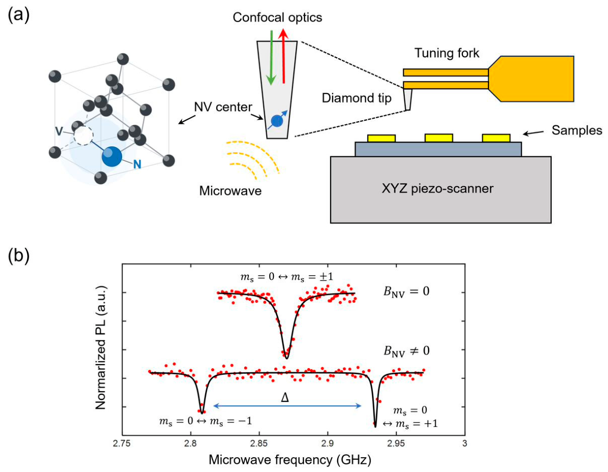
As illustrated schematically in Figure 1a, a home-built scanning magnetometry system was used in this experiment, consisting of a scanning probe microscope integrated with a confocal optical system [1,2,3]. The scanning probe employs a commercially available diamond tip (QZabre AG, Zürich, Switzerland) [24], which is attached to the end of a tuning-fork AFM probe. A single NV center is located near the apex of the diamond tip, approximately 10 nm below the surface.
To excite and read out the NV center spin state, the scanning microscope is combined with a confocal optical setup consisting of a 532 nm excitation laser (MLL-III-532, 100 mW; CNI Laser, Changchun, China), an objective lens (LCPLFLN50XLCD, Olympus, Tokyo, Japan; numerical aperture, NA = 0.7), and a single-photon counting module (SPCM-AQRH-14-FC, Excelitas Technologies, Waltham, MA, USA). Photon counting and instrument control were performed using a multifunction data acquisition module (PXIe-6363, National Instruments, Austin, TX, USA). During operation, the diamond probe (thus the NV center) is held fixed beneath the objective lens while the sample is scanned in three-dimensional space with nanometer precision using a commercial XYZ piezoelectric scanner (Attocube Systems AG, Haar, Germany; model ANSxyz50) [25].
The AFM is operated in non-contact mode using the quartz tuning fork of the diamond scanning probe (QZabre AG, Zürich, Switzerland) as the force sensor [9]. The tuning fork has a resonance frequency of 32.1 kHz with a quality factor of about 1800 and is driven continuously near resonance. As the sample approaches the tip surface, tip–sample interactions shift the resonance frequency away from the drive frequency, resulting in a reduction in oscillation amplitude. This amplitude change is maintained at a constant value through a feedback loop and is used to generate the topographic image. Scanning begins at the lower-left corner of the imaging area, where the sample is raster-scanned along the fast scan direction (the x-axis in this work) by varying the voltage applied to the piezoelectric scanner. At each fixed y-position, the sample is scanned forward along the +x direction and then backward along the −x direction, after which the sample is moved to the next y-position and the process is repeated.
The NV center is a point defect in the diamond crystal lattice consisting of a substitutional nitrogen atom adjacent to a carbon vacancy. In its negatively charged state, the NV center exhibits a spin-triplet ground state (S = 1), consisting of the spin sublevels m s = 0 and m s = ±1. In the absence of an external magnetic field, the m s = 0 state is separated from the degenerate m s = ±1 states by a zero-field splitting of 2.87 GHz at room temperature. When an external magnetic field is applied along the NV crystal axis, B N V , the m s = ±1 states experience Zeeman splitting. To drive spin transitions between the m s = 0 and m s = ±1 states, microwave radiation in the GHz frequency range, generated by a signal generator (SG384, Stanford Research Systems, Sunnyvale, CA, USA), gated by a switch (ZASWA-2-50DR+, Mini-Circuits, Brooklyn, NY, USA), and amplified (ZHL-16W-42-S+, Mini-Circuits, Brooklyn, NY, USA), is applied through an external wire or microwave antenna.
Under 532 nm laser illumination, the NV center is optically excited and subsequently emits photoluminescence (PL) in the wavelength range of approximately 637–800 nm. The PL intensity depends on the spin state, with the m s = 0 state exhibiting higher fluorescence intensity than the m s = ±1 states, typically differing by 10–30%. This spin-dependent fluorescence enables optically detected magnetic resonance (ODMR), in which the microwave frequency is swept while monitoring the PL intensity to determine the NV spin resonance frequencies [2]. Because these resonance frequencies shift through the Zeeman effect in proportion to the magnetic field projected along the NV axis, the local magnetic field can be quantitatively measured.
Figure 1b shows representative ODMR spectra measured at B N V = 0 and B N V ≠ 0. The Zeeman splitting, Δ, is extracted at each scan position to generate a static magnetic field map of the sample (e.g., Δ = 1 MHz corresponds to B N V ≈ 0.36 G). For magnetic imaging, the tip is retracted by 100 nm from the sample surface at each pixel, allowing constant-height magnetic field imaging. All measurements presented in this work were performed under ambient room-temperature conditions. All data acquisition and analysis, including the polynomial fitting described in Section 3.1, were performed using MATLAB R2024a (MathWorks, Natick, MA, USA).

2.2. Samples

In this work, three different samples were used: a commercially available AFM grating for piezoelectric hysteresis calibration, a current-carrying patterned gold device, and a hard disk sample for evaluating the effectiveness of the compensation method in both topographic and magnetic imaging.
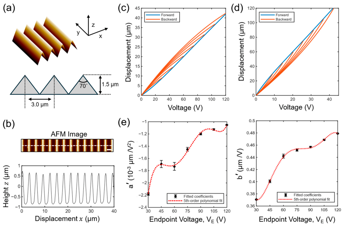
The calibration grating sample (TipsNano OÜ, Tallinn, Estonia) [26] consists of periodic wedge structures oriented along the x-axis, with a step height of 1.5 µm and a periodic spacing of 3.0 µm as shown in Figure 2a. The grating period was independently verified using a commercial AFM, yielding an average value consistent with the nominal 3.0 µm period (Figure 2b). This pre-calibrated grating structure is used to determine the polynomial relationship between the applied voltage to the x-axis piezoelectric scanner and the corresponding physical displacement, allowing extraction of the hysteresis correction parameters.
The current-carrying device consists of a patterned gold wire fabricated on a silicon substrate (see Section 3.2). The wire extends primarily along the y-direction while forming a zig-zag pattern along the x-direction. Each wire segment is 200 nm thick and 1 µm wide, with adjacent wire segments separated by 1 µm along the x-axis. Neighboring wire segments carry electrical current in opposite directions, producing a magnetic field with periodic spatial variation. During measurement, a direct current of 1.5 mA was applied to the device.
To evaluate hysteresis correction for magnetic imaging of irregular magnetic structures, a sample was prepared by cutting a section from a commercial hard disk drive. Together with the current-carrying device, the magnetic domains of the hard disk sample provide a representative test system for examining geometric distortion and evaluating the effectiveness of the compensation method in practical scanning magnetometry measurements.

3. Results and Discussion

3.1. Piezoelectric Hysteresis Compensation Using an AFM Calibration Grating

We first characterized the non-linearity and hysteresis behavior of the piezoelectric positioner using the AFM grating sample by recording its topographic image. By varying the voltage applied to the x-axis piezo scanner from 0 to 120 V, we measured the corresponding displacement along the x-axis, i.e., fast scan direction, using the pre-calibrated grating period of 3.0 µm. As shown in Figure 2c, the displacement as a function of the applied voltage exhibits distinct forward and backward branches, forming a characteristic hysteresis loop [12].
Taking the position at 0 V as the origin and denoting the applied voltage as x, the measured displacement D during the forward scan can be described by a fourth-order polynomial function,
D = ax4 + bx3 + cx2 + dx,
where the fitted coefficients are determined as a = (5.78 × 10⁻⁸ ± 0.59 × 10⁻⁸) µm/V4, b = (−2.06 × 10⁻⁵ ± 1.2 × 10⁻⁵) µm/V3, c = (2.53 × 10⁻³ ± 0.77 × 10⁻³) µm/V2, and d = (2.42 × 10⁻¹ ± 1.54 × 10⁻¹) µm/V. To compensate for the hysteresis, the inverse relation was numerically obtained by solving the polynomial equation ax4 + bx3 + cx2 + dx x t = 0 , where x t is the desired target displacement (see Appendix A for details). Figure 2d shows the resulting compensated voltage as a function of the target displacement.
For the backward scan, the voltage was swept from an endpoint voltage V E back to 0 V. As shown in Figure 2c, the backward displacement follows different trajectories depending on the endpoint voltage. In contrast to the forward scan, the backward response can be approximated by a quadratic function,
D = a′x2 + b′x + c′,
where a′ and b′ are fitting coefficients and c′ = 0, taking D = 0 at x = 0 as the reference condition.
As shown in Figure 2c, we measured the backward hysteresis curves for seven different endpoint voltages spanning 30–120 V. Each curve was first fitted using Equation (2), after which the extracted coefficients a′ and b′ were further fitted as functions of V E using polynomial expressions given by
a ( V E ) = p 5 V E 5 + p 4 V E 4 + p 3 V E 3 + p 2 V E 2 + p 1 V E + p 0
b ( V E ) = q 5 V E 5 + q 4 V E 4 + q 3 V E 3 + q 2 V E 2 + q 1 V E + q 0
where a′ and b′ are the quadratic and linear coefficients of Equation (2) (units µm/V2 and µm/V), and the fitted coefficients are:
  • p5 = 8.31 × 10⁻¹² µm/V7, p4 = −3.24 × 10⁻⁹ µm/V6, p3 = 4.82 × 10⁻⁷ µm/V5, p2 = 3.41 × 10⁻⁵ µm/V4, p1 = 1.15 × 10⁻³ µm/V3, p0 = 1.66 × 10⁻² µm/V2;
  • q5 = 4.93 × 10⁻¹⁰ µm/V6, q4 = 1.9 × 10⁻⁷ µm/V5, q3 = 2.79 × 10⁻⁵ µm/V4, q2 = 1.91 × 10⁻³ µm/V3, q1 = 5.81 × 10⁻² µm/V2, q0 = 1.01 µm/V.
Similar to the forward scan case, the compensated voltage for the backward scan was obtained by solving the inverse relation
x = [−b′ + √ (b′2 + 4axt′)]/(2a′),
where x t represents the target displacement during backward scanning. The calculated compensated voltages are shown in Figure 2d.
Note that the rationale for selecting the fourth-order polynomial for the forward scan and the quadratic polynomial for the backward scan is provided in the Supplementary Materials (Supplementary Note S1). The Supplementary Materials also include a comparison of the proposed method with a simpler linear correction approach (Supplementary Note S2).
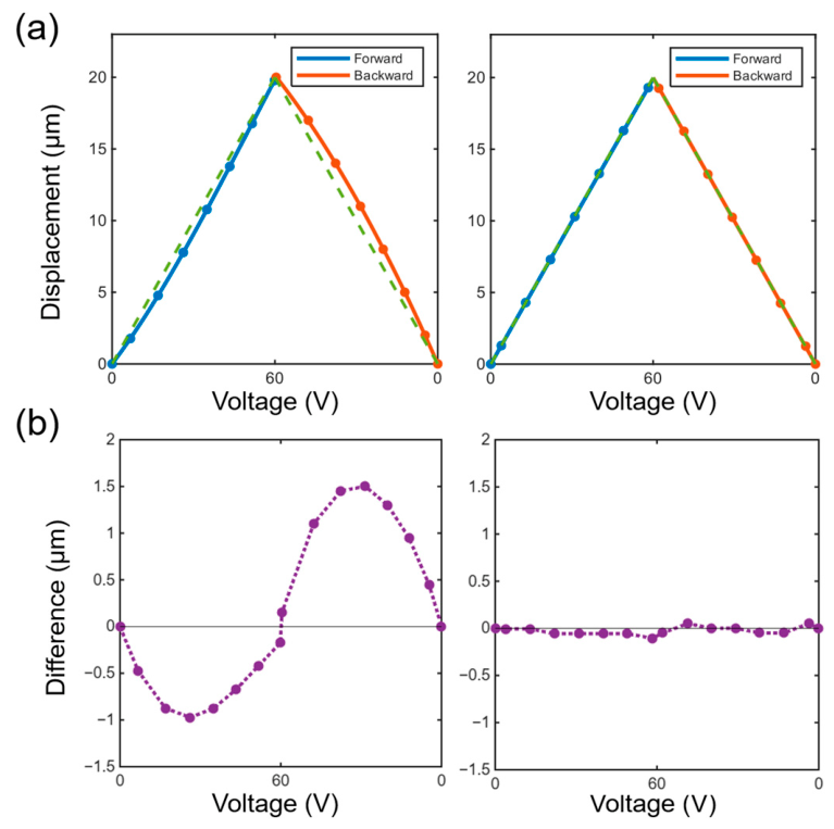
To verify the effectiveness of the compensation method, we compared the measured displacement before and after correction by scanning the grating sample while sweeping the forward scan voltage from 0 to 60 V and subsequently scanning backward from 60 V to 0 V. In Figure 3a, the dashed lines indicate the ideal linear response without hysteresis, while the markers and solid lines represent the experimentally measured displacement. As clearly shown in Figure 3b, before compensation, the deviation between the measured and ideal displacement reaches a maximum error of approximately ±1.4 µm. After applying the compensation method, this error is significantly reduced to less than ±0.1 µm in both scan directions. These results confirm that the proposed calibration procedure effectively linearizes the piezoelectric positioner response and substantially suppresses hysteresis-induced positioning errors during scanning [13,22].
Note that both the calibration and the imaging measurements presented in the following sections were performed using the same scanner under identical environmental conditions. During the ~10 min calibration of each scan line, the measured thermal drift remained effectively linear and therefore affected only the linear coefficient of the displacement–voltage relation, without influencing the higher-order coefficients used for hysteresis compensation. Furthermore, the calibration remains valid as long as the scanner characteristics and operating conditions remain unchanged. Recalibration is recommended following significant changes in temperature, scan rate, or prolonged operation of the scanner.

3.2. Magnetic Imaging on a Current-Carrying Gold Wire

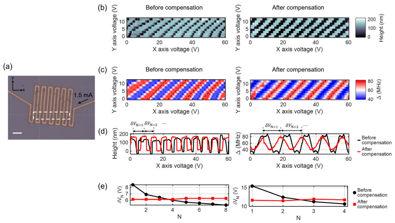
To evaluate the proposed compensation method in practical scanning magnetometry experiments, we first used the current-carrying patterned gold wire device shown in Figure 4a. This sample produces both a periodic topographic structure and, when an electric current is applied, a periodic magnetic field distribution. Therefore, any deviation from the expected periodicity in either image directly reflects distortion caused by the piezoelectric scanner. As described in Section 2.1, the oscillation amplitude of the AFM probe is used to record the topographic image, while the Zeeman splitting obtained from ODMR measurements, Δ, is used to generate the magnetic field image, which gives the field component along the NV axis [1,2]. The scan range was set to V x = 0–60 V (401 pixels) along the x-direction (fast scan axis) and V y = 0–12 V (9 pixels) along the y-direction (slow scan axis).
Figure 4b,c show representative forward-scan topographic and magnetic field images, respectively, measured within the dashed region indicated in Figure 4a, before and after applying the compensation. Before compensation, both the topographic and magnetic images exhibit periodic features that are bent and unevenly spaced rather than straight and uniformly distributed. Because the gold wire pattern is tilted by approximately 6° relative to the fast scan direction, individual wire segments appear slightly diagonal in the scanned image. At lower V y values, the spacing between neighboring wire segments gradually increases up to V x ~30 V and then decreases at higher V x values, resulting in a characteristic bending of the wire segments. At larger V y values, wire segments at V x < 30 V appear increasingly tilted toward the +x direction compared to those at lower V y , and, for V x > 30 V, both the tilt angle and the spacing between neighboring segments gradually decrease. The dashed lines shown in the magnetic images of Figure 4c serve as visual guides indicating the actual alignment of the wire pattern.
This distortion behavior can be directly explained by the voltage-dependent displacement error shown previously in Figure 3b, where the displacement error reaches its maximum near 30 V and continuously decreases toward zero as the voltage approaches 60 V. In contrast, after applying the compensation method, both the topographic and magnetic images recover straight and uniformly spaced features, demonstrating effective removal of hysteresis-induced geometric distortion. Note that, since the detailed hysteresis behavior depends on the specific characteristics of each piezoelectric scanner, calibration and compensation must be performed individually for each scanning magnetometry system.
For further quantitative comparison, Figure 4d shows linecuts extracted from both topographic and magnetic images at V y = 10.5 V. To quantify the distortion, Figure 4e plots the spacing between neighboring wire segments, denoted as δ V N , where N is the segment index starting from the first segment at low V x . The spacing values are extracted from the center positions of the topographic plateaus and from the peak positions in the magnetic field images. In the uncompensated topographic image, δ V N starts at a relatively large value, decreases monotonically, and reaches the designed periodic spacing of 2 µm (i.e., 1 µm wire width plus 1 µm spacing) around N = 4, corresponding approximately to V x = 30 V. At larger N values, corresponding to higher V x , the spacing continues to decrease below the expected value. A similar trend is observed in the uncompensated magnetic image.
After applying compensation, both topographic and magnetic images show nearly uniform spacing across the entire scan range, closely matching the designed device geometry. The remaining small deviations can be attributed primarily to thermal drift of the sample stage under ambient conditions, independently measured to be approximately 0.004 µm/min along the x direction and 0.013 µm/min along the y direction. For the slow (y) axis, only the forward displacement–voltage relation is required because the scanner advances monotonically without a forward–backward voltage sweep. The same calibration obtained from the x-axis is applied to the y-axis, since both axes employ identical piezoelectric actuators, and the absence of noticeable distortion in the gold-wire images supports the validity of this approximation under the present experimental conditions.
These results clearly demonstrate that the proposed compensation method effectively suppresses piezoelectric hysteresis and significantly improves image fidelity in NV-based scanning magnetometry measurements.

3.3. Magnetic Imaging on a Hard Disk

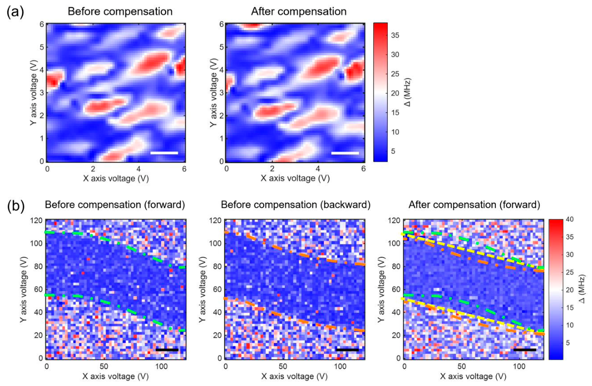
In addition to the measurements on the current-carrying device, we performed magnetic imaging of magnetic domains in a hard disk sample [1,2,23]. In this experiment, we compare the effect of piezoelectric hysteresis between small-area and large-area scanning measurements. Figure 5a shows forward-scan magnetic images acquired over a small scan area ( V x = V y = 0–6 V, 61 × 61 pixels) before and after applying the compensation. Because the applied voltage range is sufficiently small, hysteresis-induced distortion is negligible and no clear difference is observed between the uncompensated and compensated images. The small differences that remain are attributed primarily to thermal drift between the two sequential measurements.
In contrast, Figure 5b shows magnetic images acquired over a large scan area ( V x = V y = 0–120 V, 51 × 51 pixels), displaying the forward scan before compensation, backward scan before compensation, and forward scan after compensation from left to right, respectively. For this measurement, we intentionally selected a region containing relatively large magnetic domains with approximately straight domain boundaries in order to clearly visualize geometric distortion. The uncompensated images exhibit noticeable distortion of the domain boundaries, with different distortion patterns observed in the forward and backward scan images, consistent with the hysteresis behavior shown previously in Figure 2b and Figure 3b. For example, in the forward scan image, the piezoelectric scanner produces less displacement than the ideal response below V x = 60 V, while the displacement error gradually decreases at higher voltages. As a result, cumulative displacement errors cause each domain boundary to shift and bend toward the +x direction. In contrast, the backward scan follows a different hysteresis branch that depends on the endpoint voltage V E , as shown in Figure 2b, resulting in an opposite distortion pattern compared to the forward scan image.
After applying the compensation, however, the magnetic image clearly shows that the straight domain boundaries are successfully recovered. The dash-dotted guide lines indicate the distorted boundaries observed in the uncompensated images, which exhibit upward deflection in the forward scan and downward deflection in the backward scan relative to the ideal straight boundary indicated by the dashed line. These distortion trends are consistent with the piezoelectric hysteresis characteristics shown in Figure 2b. The results demonstrate that the proposed method successfully removes hysteresis-induced distortion not only for patterned current-carrying devices but also for irregular magnetic samples encountered in practical scanning magnetometry experiments.

4. Conclusions

In conclusion, we have demonstrated a software-based polynomial compensation method for correcting piezoelectric hysteresis in NV-based scanning magnetometry. By calibrating and analytically inverting the forward and backward displacement-voltage relations, the method compensates nonlinear positioning errors through the applied driving voltage alone, without requiring additional hardware or closed-loop position control. The proposed approach was experimentally validated using a current-carrying gold device and magnetic domains in a hard-disk sample. The compensated scans exhibit substantially improved geometric fidelity in both topographic and magnetic-field images by effectively removing hysteresis-induced image distortion and non-uniform pixel spacing. Because the method is implemented entirely in software, it can be readily integrated into existing open-loop scanning magnetometry systems with minimal modification. More generally, it provides a simple and cost-effective approach for improving the quantitative accuracy of large-area scanning measurements and can be extended to other scanning probe-based quantum sensing and imaging platforms.

Supplementary Materials

The following supporting information can be downloaded at: https://www.mdpi.com/article/10.3390/app16157831/s1.

Author Contributions

S.L. (Seokmin Lee), Y.L., S.J., S.K. (Sunwoo Kim), S.L. (Seonho Lee), and D.L. conceived and designed the experiments; S.L. (Seokmin Lee), and Y.L. constructed the experimental setup; S.L. (Seokmin Lee), Y.L., S.J., S.K. (Sunwoo Kim), and S.L. (Seonho Lee) performed the experiments and analysis; S.-K.S. (Seok-Kyun Son), A.J.H., and D.L. directed and supervised the project; S.L. (Seokmin Lee), Y.L., and D.L. wrote the manuscript with contributions from all co-authors. All authors have read and agreed to the published version of the manuscript.

Funding

This work was supported by the Korea Research Institute for Defense Technology Planning and Advancement (KRIT)—grant funded by the Defense Acquisition Program Administration (DAPA) (Grant No. KRIT-CT-23-031), the National Research Foundation of Korea (NRF) (Grant No. RS-2022-NR068822), and the Institute of Information & Communications Technology Planning & Evaluation (IITP) (Grant No. IITP-2026-RS-2020-II201606) funded by the Korean government (Ministry of Science and ICT). S.L., Y.L., S.J., S.K., D.L., and A.J.H. are also thankful for support from the Institute for Basic Science (Grant No. IBS-R027-D1).

Institutional Review Board Statement

Not applicable.

Informed Consent Statement

Not applicable.

Data Availability Statement

The data presented in this study are available on request from the corresponding author due to privacy concerns.

Conflicts of Interest

The authors declare no conflicts of interest.

Abbreviations

The following abbreviations are used in this manuscript:
NVNitrogen-vacancy
AFMAtomic force microscope
SPMScanning probe microscopy
NANumerical aperture
PLPhotoluminescence
ODMROptically detected magnetic resonance

Appendix A. Closed-Form Forward Inversion

The applied voltage corresponding to a target forward displacement x t is obtained by solving the quartic equation
ax4 + bx3 + cx2 + dx + e = 0,
where e   =   x t . The closed form solutions are given by
x = −b/(4a) − S ± ½√(−4S2 − 2p + q/S), and x = −b/(4a) + S ± ½√(−4S2 − 2pq/S),
where
p = (8ac − 3b2)/(8a2), q = (b3 − 4abc + 8a2d)/(8a3),
S = ½√(−⅔p + (1/(3a))(Q + Δ0/Q)), Q = ∛((Δ1 + √(Δ12 − 4Δ03))/2),
Δ0 = c2 − 3bd + 12ae, and Δ1 = 2c3 − 9bcd + 27b2e + 27ad2 − 72ace.
Among the four solutions, the physically relevant one is selected as the single real value lying within the scan voltage range.

References

  1. Balasubramanian, G.; Chan, I.Y.; Kolesov, R.; Al-Hmoud, M.; Tisler, J.; Shin, C.; Kim, C.; Wojcik, A.; Hemmer, P.R.; Krueger, A.; et al. Nanoscale Imaging Magnetometry with Diamond Spins under Ambient Conditions. Nature 2008, 455, 648–651. [Google Scholar] [CrossRef] [PubMed]
  2. Rondin, L.; Tetienne, J.-P.; Hingant, T.; Roch, J.-F.; Maletinsky, P.; Jacques, V. Magnetometry with Nitrogen-Vacancy Defects in Diamond. Rep. Prog. Phys. 2014, 77, 056503. [Google Scholar] [CrossRef] [PubMed]
  3. Maletinsky, P.; Hong, S.; Grinolds, M.S.; Hausmann, B.; Lukin, M.D.; Walsworth, R.L.; Loncar, M.; Yacoby, A. A Robust Scanning Diamond Sensor for Nanoscale Imaging with Single Nitrogen-Vacancy Centres. Nat. Nanotechnol. 2012, 7, 320–324. [Google Scholar] [CrossRef] [PubMed]
  4. Gross, I.; Akhtar, W.; Garcia, V.; Martínez, L.J.; Chouaieb, S.; Garcia, K.; Carrétéro, C.; Barthélémy, A.; Appel, P.; Maletinsky, P.; et al. Real-Space Imaging of Non-Collinear Antiferromagnetic Order with a Single-Spin Magnetometer. Nature 2017, 549, 252–256. [Google Scholar] [CrossRef] [PubMed]
  5. Thiel, L.; Wang, Z.; Tschudin, M.A.; Rohner, D.; Gutiérrez-Lezama, I.; Ubrig, N.; Gibertini, M.; Giannini, E.; Morpurgo, A.F.; Maletinsky, P. Probing Magnetism in 2D Materials at the Nanoscale with Single-Spin Microscopy. Science 2019, 364, 973–976. [Google Scholar] [CrossRef] [PubMed]
  6. Ku, M.J.H.; Zhou, T.X.; Li, Q.; Shin, Y.J.; Shi, J.K.; Burch, C.; Anderson, L.E.; Pierce, A.T.; Xie, Y.; Hamo, A.; et al. Imaging Viscous Flow of the Dirac Fluid in Graphene. Nature 2020, 583, 537–541. [Google Scholar] [CrossRef] [PubMed]
  7. Xu, Y.; Zhang, W.; Tian, C. Recent Advances on Applications of NV Magnetometry in Condensed Matter Physics. Photonics Res. 2023, 11, 393–412. [Google Scholar] [CrossRef]
  8. Christensen, D.V.; Staub, U.; Devidas, T.R.; Kalisky, B.; Nowack, K.C.; Webb, J.L.; Andersen, U.L.; Huck, A.; Broadway, D.A.; Wagner, K.; et al. 2024 Roadmap on Magnetic Microscopy Techniques and Their Applications in Materials Science. J. Phys. Mater. 2024, 7, 032501. [Google Scholar] [CrossRef]
  9. Binnig, G.; Quate, C.F.; Gerber, C. Atomic Force Microscope. Phys. Rev. Lett. 1986, 56, 930–933. [Google Scholar] [CrossRef] [PubMed]
  10. Wiesendanger, R. Scanning Probe Microscopy and Spectroscopy: Methods and Applications; Cambridge University Press: Cambridge, UK, 1994; ISBN 978-0-521-42847-7. [Google Scholar]
  11. Habibullah, H. 30 Years of Atomic Force Microscopy: Creep, Hysteresis, Cross-Coupling, and Vibration Problems of Piezoelectric Tube Scanners. Measurement 2020, 159, 107776. [Google Scholar] [CrossRef]
  12. Croft, D.; Shedd, G.; Devasia, S. Creep, Hysteresis, and Vibration Compensation for Piezoactuators: Atomic Force Microscopy Application. J. Dyn. Syst. Meas. Control 2001, 123, 35–43. [Google Scholar] [CrossRef]
  13. Sun, B.; Cao, L.; Lu, Z.; Xie, C.; Song, Z.; Weng, Z.; Wang, Z. Modeling and Correction of Image Pixel Hysteresis in Atomic Force Microscopy. Ultramicroscopy 2020, 213, 112992. [Google Scholar] [CrossRef] [PubMed]
  14. Kanchan, M.; Santhya, M.; Bhat, R.; Naik, N. Application of Modeling and Control Approaches of Piezoelectric Actuators: A Review. Technologies 2023, 11, 155. [Google Scholar] [CrossRef]
  15. Fleming, A.J.; Leang, K.K. Charge Drives for Scanning Probe Microscope Positioning Stages. Ultramicroscopy 2008, 108, 1551–1557. [Google Scholar] [CrossRef] [PubMed]
  16. Leang, K.K.; Devasia, S. Feedback-Linearized Inverse Feedforward for Creep, Hysteresis, and Vibration Compensation in AFM Piezoactuators. IEEE Trans. Control Syst. Technol. 2007, 15, 927–935. [Google Scholar] [CrossRef]
  17. Devasia, S.; Eleftheriou, E.; Moheimani, S.O.R. A Survey of Control Issues in Nanopositioning. IEEE Trans. Control Syst. Technol. 2007, 15, 802–823. [Google Scholar] [CrossRef]
  18. Qin, Y.; Zhang, Y.; Duan, H.; Han, J. High-Bandwidth Hysteresis Compensation of Piezoelectric Actuators via Multilayer Feedforward Neural Network Based Inverse Hysteresis Modeling. Micromachines 2021, 12, 1325. [Google Scholar] [CrossRef] [PubMed]
  19. Nguyen, T.T.; Otieno, L.O.; Juma, O.M.; Nguyen, T.N.; Lee, Y.J. Nonlinear Modeling of a Piezoelectric Actuator-Driven High-Speed Atomic Force Microscope Scanner Using a Variant DenseNet-Type Neural Network. Actuators 2024, 13, 391. [Google Scholar] [CrossRef]
  20. Preisach, F. Über die magnetische Nachwirkung. Z. Phys. 1935, 94, 277–302. [Google Scholar] [CrossRef]
  21. Al Janaideh, M.; Rakheja, S.; Su, C.-Y. An Analytical Generalized Prandtl–Ishlinskii Model Inversion for Hysteresis Compensation in Micropositioning Control. IEEE/ASME Trans. Mechatron. 2011, 16, 734–744. [Google Scholar] [CrossRef]
  22. Wang, Y.; Wu, S.; Xu, L.; Zeng, Y. A New Precise Positioning Method for Piezoelectric Scanner of AFM. Ultramicroscopy 2019, 196, 67–73. [Google Scholar] [CrossRef] [PubMed]
  23. Rugar, D.; Mamin, H.J.; Guethner, P.; Lambert, S.E.; Stern, J.E.; McFadyen, I.; Yogi, T. Magnetic Force Microscopy: General Principles and Application to Longitudinal Recording Media. J. Appl. Phys. 1990, 68, 1169–1183. [Google Scholar] [CrossRef]
  24. QZabre, A.G. Scanning Diamond Probes (QST). Available online: https://www.qzabre.com/QST (accessed on 24 June 2026).
  25. Attocube Systems AG. ANSxyz50/LT—XYZ Scanner Made of Titanium. Available online: https://www.attocube.com/en/products/nanopositioners/low-temperature-nanopositioners/ansxyz50lt-xyz-scanner-made-titanium (accessed on 24 June 2026).
  26. TipsNano, O.Ü. AFM Calibration Gratings. Available online: https://www.tipsnano.com (accessed on 24 June 2026).
Figure 1. NV-based scanning magnetometry. (a) Schematics of the scanning magnetometry setup based on a diamond NV center. A fabricated diamond tip hosting a single NV center near the tip apex is attached to a tuning-fork AFM probe. An XYZ piezo-scanner is used to move the sample with nanometer-scale precision while the tip remains fixed. Confocal optics are used to excite the NV center with a 532 nm laser (green arrow) and to collect its photoluminescence (PL, red arrow). An external wire generates GHz-frequency microwave radiation to drive the NV spin transitions m s = 0 ↔ m s = −1 and m s = 0 ↔ m s = +1. (b) Representative ODMR spectra at zero and non-zero magnetic field, B N V . At B N V = 0, the degenerate spin transitions ( m s = 0 ↔ m s = ±1) overlap, whereas at B N V ≠ 0, the transitions split into m s = 0 ↔ m s = −1 and m s = 0 ↔ m s = +1 due to the Zeeman effect. The Zeeman splitting, Δ, is measured at each scan position to reconstruct the static magnetic field distribution during scanning measurements. Red dots, measured data; black solid lines, fits.
Applsci 16 07831 g001
Figure 2. Piezo-hysteresis compensation using an AFM grating. (a) Schematics of the AFM calibration grating. The grating consists of periodic wedge structures along the x-axis (fast scan direction), with a step height of 1.5 µm and a periodic spacing of 3.0 µm. (b) AFM image of the calibration grating (upper panel) and the corresponding line profile measured along the dashed line (lower panel). The grating period of approximately 3.0 µm was independently verified using a commercial AFM. Scale bar = 2 µm. (c) Measured displacement along the x-axis as a function of the applied voltage to the X piezo scanner for forward and backward scans, showing the characteristic hysteresis behavior. (d) Compensated voltage as a function of the target displacement. Polynomial inversion using quartic (forward scan) and quadratic (backward scan) fitting functions is used to determine the corrected voltage required to obtain the desired displacement. (e) Polynomial fit coefficients describing the backward hysteresis response as a function of the endpoint voltage, V E . The quadratic coefficients a′ (left) and linear coefficient b′ (right) are extracted from the backward scan curves and fitted as fifth-order polynomial functions of V E . See the main text for details.
Applsci 16 07831 g002
Figure 3. Comparison of displacement before and after hysteresis compensation. (a) Measured displacement along the x-axis as a function of the applied voltage before (left) and after (right) hysteresis compensation. The dashed lines indicate the ideal linear response without hysteresis, while the markers and solid lines represent the experimentally measured displacement. (b) Difference between the measured and ideal displacement shown in (a) as a function of the applied voltage before (left) and after (right) compensation.
Applsci 16 07831 g003
Figure 4. Topographic and magnetic imaging on a current-carrying gold wire. (a) Optical image of the fabricated gold wire sample. A direct current of 1.5 mA is applied to generate a static Oersted magnetic field. Scale bar = 5 µm. (b,c) Topographic (b) and magnetic field, Δ, (c) images of the marked region in (a) before (left) and after (right) hysteresis compensation. The dashed lines in (c) serve as visual guides indicating the actual alignment of the wire pattern. (d) Linecut data extracted from the topographic and magnetic images shown in (b,c) at the y-axis voltage V y = 10.5 V. Black and red curves correspond to the data before and after compensation, respectively. (e) Spacing between neighboring wire segments ( δ V N ) plotted as a function of the segment index (N) starting from the first segment at low x-axis voltage ( V x ). Black and red markers correspond to the values extracted from (d) before and after compensation, respectively.
Applsci 16 07831 g004
Figure 5. Magnetic imaging on a hard disk. (a) Forward-scan magnetic images, Δ, acquired over a small scan area of the hard disk sample ( V x = V y = 0–6 V, 61 × 61 pixels) before (left) and after (right) hysteresis compensation. Scale bar = 3 µm. (b) Magnetic images of hard disk domains acquired over a large scan area ( V x = V y = 0–120 V, 51 × 51 pixels), showing the forward scan (left) and backward scan (middle) before compensation, and the forward scan after compensation (right). The dash-dotted and dashed lines are visual guides indicating the domain boundaries in the uncompensated images and the compensated image, respectively. Scale bar = 50 µm.
Applsci 16 07831 g005
Disclaimer/Publisher’s Note: The statements, opinions and data contained in all publications are solely those of the individual author(s) and contributor(s) and not of MDPI and/or the editor(s). MDPI and/or the editor(s) disclaim responsibility for any injury to people or property resulting from any ideas, methods, instructions or products referred to in the content.